

Motorola MRF20060S, MRF20060 Datasheet

SEMICONDUCTOR TECHNICAL DATA
The RF Sub–Micron Bipolar Line
Order this document
by MRF20060/D
The MRF20060 and MRF20060S are designed for broadband commercial
and industrial applications at frequencies from 1800 to 2000 MHz. The high
gain, excellent linearity and broadband performance of these devices make
them ideal for large–signal, common emitter class A and class AB amplifier
applications. These devices are suitable for frequency modulated, amplitude
modulated and multi–carrier base station RF power amplifiers.
• Guaranteed Two–tone Performance at 2000 MHz, 26 Volts
Output Power — 60 Watts (PEP)
Power Gain — 9 dB
Efficiency — 33%
Intermodulation Distortion — –30 dBc
• Characterized with Series Equivalent Large–Signal Impedance Parameters
• S–Parameter Characterization at High Bias Levels
• Excellent Thermal Stability
• Capable of Handling 3:1 VSWR @ 26 Vdc, 2000 MHz, 60 Watts (PEP)
Output Power
• Designed for FM, TDMA, CDMA and Multi–Carrier Applications
60 W, 2000 MHz
RF POWER
BROADBAND
NPN BIPOLAR
CASE 451–04, STYLE 1
(MRF20060)
MAXIMUM RATINGS
Rating Symbol Value Unit
Collector–Emitter Voltage (IB = 0 mA) V
Collector–Emitter Voltage V
Collector–Base Voltage V
Collector–Emitter Voltage (RBE = 100 Ohm) V
Base–Emitter Voltage V
Collector Current – Continuous I
Total Device Dissipation @ TC = 25°C
Derate above 25°C
Storage Temperature Range T
Operating Junction Temperature T
THERMAL CHARACTERISTICS
Rating Symbol Max Unit
Thermal Resistance, Junction to Case R
CEO
CES
CBO
CER
EB
C
P
D
stg
J
θJC
CASE 451A–01, STYLE 1
(MRF20060S)
25 Vdc
60 Vdc
60 Vdc
30 Vdc
–3 Vdc
8 Adc
250
1.43
– 65 to +150 °C
200 °C
0.7 °C/W
Watts
W/°C
Motorola, Inc. 1997
MRF20060 MRF20060SMOTOROLA RF DEVICE DATA
1

ELECTRICAL CHARACTERISTICS (T
Characteristic
= 25°C unless otherwise noted)
C
OFF CHARACTERISTICS
Collector–Emitter Breakdown V oltage
(IC = 50 mAdc, IB = 0)
Collector–Emitter Breakdown Voltage
(IC = 50 mAdc, VBE = 0)
Collector–Base Breakdown Voltage
(IC = 50 mAdc, IE = 0)
Reverse Base–Emitter Breakdown Voltage
(IB = 10 mAdc, IC = 0)
Zero Base Voltage Collector Leakage Current
(VCE = 30 Vdc, VBE = 0)
ON CHARACTERISTICS
DC Current Gain
(VCE = 5 Vdc, IC = 1 Adc)
DYNAMIC CHARACTERISTICS
Output Capacitance
(VCB = 26 Vdc, IE = 0, f = 1.0 MHz)
(1)
FUNCTIONAL TESTS (In Motorola T est Fixture)
Common–Emitter Amplifier Power Gain
(VCC = 26 Vdc, P
f1 = 2000.0 MHz, f2 = 2000.1 MHz)
Collector Efficiency
(VCC = 26 Vdc, P
f1 = 2000.0 MHz, f2 = 2000.1 MHz)
Intermodulation Distortion
(VCC = 26 Vdc, P
f1 = 2000.0 MHz, f2 = 2000.1 MHz)
Input Return Loss
(VCC = 26 Vdc, P
f1 = 2000.0 MHz, f2 = 2000.1 MHz)
Output Mismatch Stress
(VCC = 26 Vdc, P
f1 = 2000.0 MHz, f2 = 2000.1 MHz, VSWR = 3:1, All Phase
Angles at Frequency of Test)
(1) For Information Only. This Part Is Collector Matched.
= 60 Watts (PEP), ICQ = 200 mA,
out
= 60 Watts (PEP), ICQ = 200 mA,
out
= 60 Watts (PEP), ICQ = 200 mA,
out
= 60 Watts (PEP), ICQ = 200 mA,
out
= 60 Watts (PEP), ICQ = 200 mA,
out
Symbol Min Typ Max Unit
V
(BR)CEO
V
(BR)CES
V
(BR)CBO
V
(BR)EBO
I
CES
h
FE
C
ob
G
pe
η 33 35 — %
IMD — –33 –30 dB
IRL 12 19 — dB
ψ
25 26 — Vdc
60 69 — Vdc
60 69 — Vdc
3 3.5 — Vdc
— — 10 mAdc
20 40 80 —
— 55 — pF
9 9.4 — dB
No Degradation in Output Power
MRF20060 MRF20060S
2
MOTOROLA RF DEVICE DATA
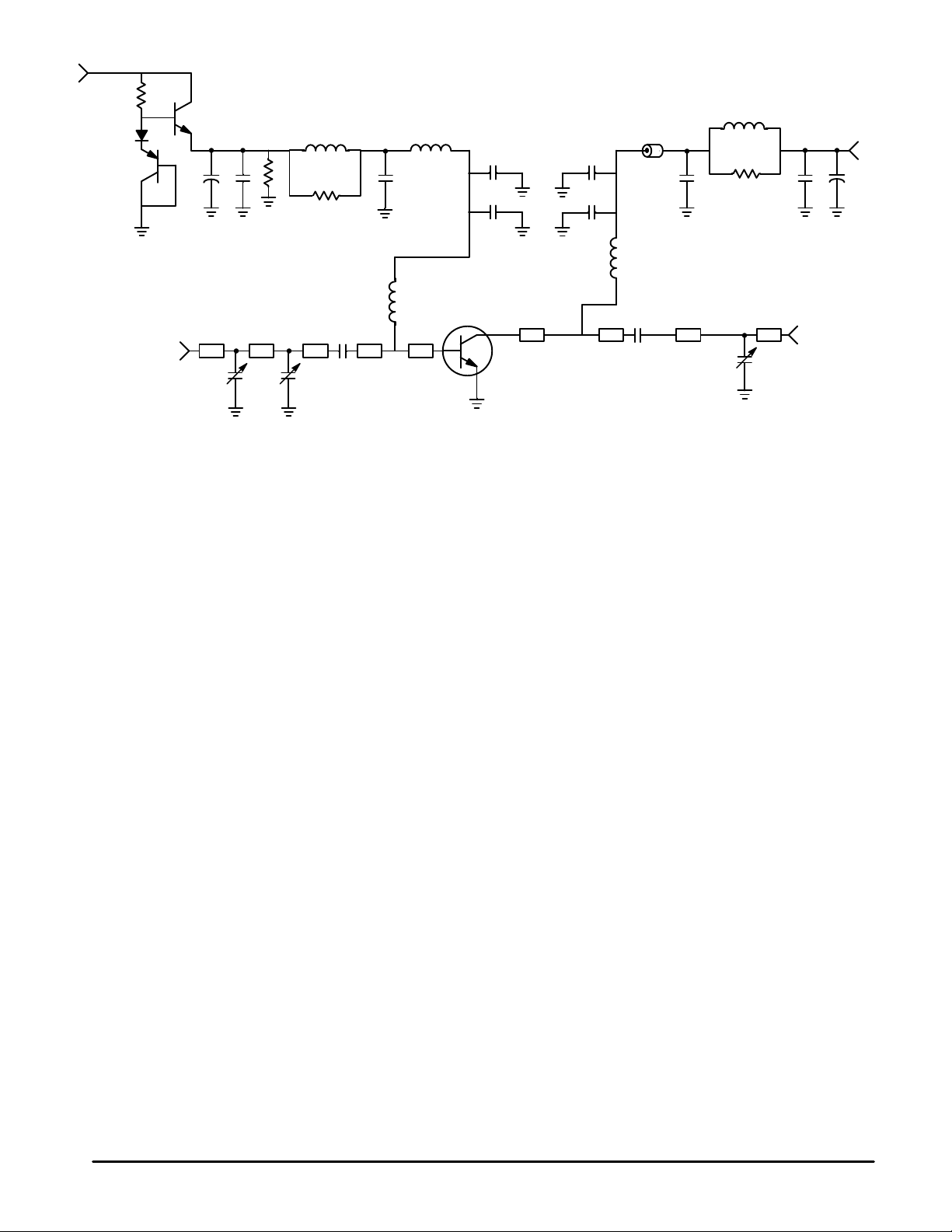
V
BB
R1
D1
Q1
RF
INPUT
Q2
L1 L3
+
C3
C1
R2
Z1 Z2 Z3 Z4 Z5
C2 C4
R3
L2
C5
C6
C7
C8
Z6 Z7 Z9
DUT
C9
C10
B1
C12
L4
C11
L5
R4
Z10
C13
C14
+
C15
RF
OUTPUT
V
CC
B1 Ferrite Bead, P/N 5659065/3B, Ferroxcube
C1 100 µF, 50 V, Electrolytic Capacitor, Mallory
C2, C4, C13 0.6–4.0 pF, Variable Capacitor, Gigatrim, Johanson
C3, C14 0.1 µF, Chip Capacitor, Kemit
C5 15 pF, B Case Chip Capacitor, A TC
C6, C12 1000 pF, B Case Chip Capacitor, ATC
C7, C9 91 pF, B Case Chip Capacitor, ATC
C8, C10 24 pF, B Case Chip Capacitor, ATC
C11 13 pF, B Case Chip Capacitor, ATC
C15 470 µF, 50 V, Electrolytic Capacitor, Mallory
Figure 1. Class AB, 1.93 – 2 GHz T est Fixture Electrical Schematic
D1 Diode, Motorola (MUR3160T3)
L1, L5 12 Turns, 22 AWG, 0.140″ Choke
L2, L4 .5 inch of 20 AWG, ID Choke
L3 12.5 nH Inductor
R1 2 x 130 Ω, 1/8 W Chip Resistor, Rohm
R2 2 x 100 Ω, 1/8 W Chip Resistor, Rohm
R3, R4 10 Ω, 1/2 W, Resistor
Q1 Transistor, PNP Motorola (BD136)
Q2 Transistor, NPN Motorola (MJD47)
Board Glass Teflon, Arlon GX–0300–55–22, εr = 2.55
MRF20060 MRF20060SMOTOROLA RF DEVICE DATA
3
 Loading...