

Motorola MRF16006 Datasheet

1
MRF16006MOTOROLA RF DEVICE DATA
The RF Line
RF Power Transistor
Designed for 28 Volt microwave large–signal, common base, Class–C CW
amplifier applications in the range 1600 – 1640 MHz.
• Specified 28 Volt, 1.6 GHz Class–C Characteristics
Output Power = 6 Watts
Minimum Gain = 7.4 dB, @ 6 Watts
Minimum Efficiency = 40% @ 6 Watts
• Characterized with Series Equivalent Large–Signal Parameters from
1500 MHz to 1700 MHz
• Silicon Nitride Passivated
• Gold Metallized, Emitter Ballasted for Long Life and Resistance to
Metal Migration
• Circuit board photomaster available upon request by contacting
RF Tactical Marketing in Phoenix, AZ.
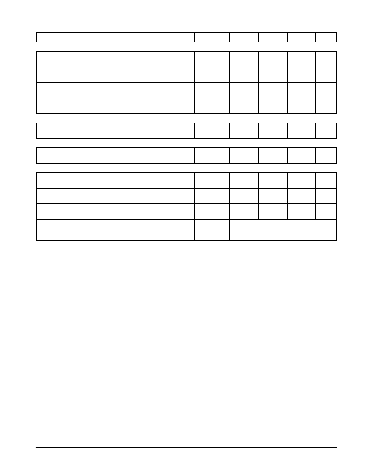
MAXIMUM RATINGS
(TJ = 25°C unless otherwise noted)
Rating
Symbol Value Unit
Collector–Emitter Voltage V
CES
60 Vdc
Emitter–Base Voltage V
EBO
4.0 Vdc
Collector–Current I
C
1.0 Adc
Total Device Dissipation @ TC = 25°C
Derate above 25°C
P
D
26
0.15
Watts
W/°C
Storage Temperature Range T
stg
–65 to +150 °C
THERMAL CHARACTERISTICS
Thermal Resistance — Junction to Case (1) (2) R
θJC
6.8 °C/W
(1) Thermal measurement performed using CW RF operating condition.
(2) Thermal resistance is determined under specified RF operating conditions by infrared measurement techniques.
Order this document
by MRF16006/D
SEMICONDUCTOR TECHNICAL DATA
CASE 395C–01, STYLE 2
6.0 WATTS, 1.6 GHz
RF POWER TRANSISTOR
NPN SILICON
Motorola, Inc. 1995
REV 2
MRF16006
2
MOTOROLA RF DEVICE DATA
ELECTRICAL CHARACTERISTICS (T
C
= 25°C unless otherwise noted)
Characteristic
Symbol Min Typ Max Unit
OFF CHARACTERISTICS
Collector–Emitter Breakdown Voltage
(IC = 40 mAdc, VBE = 0)
V
(BR)CES
55 — —
Vdc
Collector–Base Breakdown Voltage
(IC = 40 mAdc, IE = 0)
V
(BR)CBO
55 — —
Vdc
Emitter–Base Breakdown Voltage
(IE = 2.5 mAdc, IC = 0)
V
(BR)EBO
4.0 — —
Vdc
Collector Cutoff Current
(VCE = 28 Vdc, VBE = 0)
I
CES
— — 2.5
mAdc
ON CHARACTERISTICS
DC Current Gain
(ICE = 0.2 Adc, VCE = 5.0 Vdc)
h
FE
20 — 80
—
DYNAMIC CHARACTERISTICS
Output Capacitance
(VCB= 28 Vdc, f = 1.0 MHz)
C
ob
11 — —
pf
FUNCTIONAL TESTS
Common–Base Amplifier Power Gain
(VCC = 28 Vdc, P
out
= 6 Watts, f = 1600/1640 MHz)
G
pe
7.4 — —
dB
Collector Efficiency
(VCC = 28 Vdc, P
out
= 6 Watts, f = 1600/1640 MHz)
η
40 45 —
%
Return Loss
(VCC = 28 Vdc, P
out
= 6 Watts, f = 1600/1640 MHz)
I
RL
— 8.0 —
dB
Output Mismatch Stress
(VCC = 28 Vdc, P
out
= 6 Watts, f = 1600 MHz, Load
VSWR = 3:1 all phase angles at frequency of test)
ψ
No Degradation in Output Power
 Loading...