

Motorola MRF158 Datasheet
1
MRF158MOTOROLA RF DEVICE DATA
The RF TMOS Line
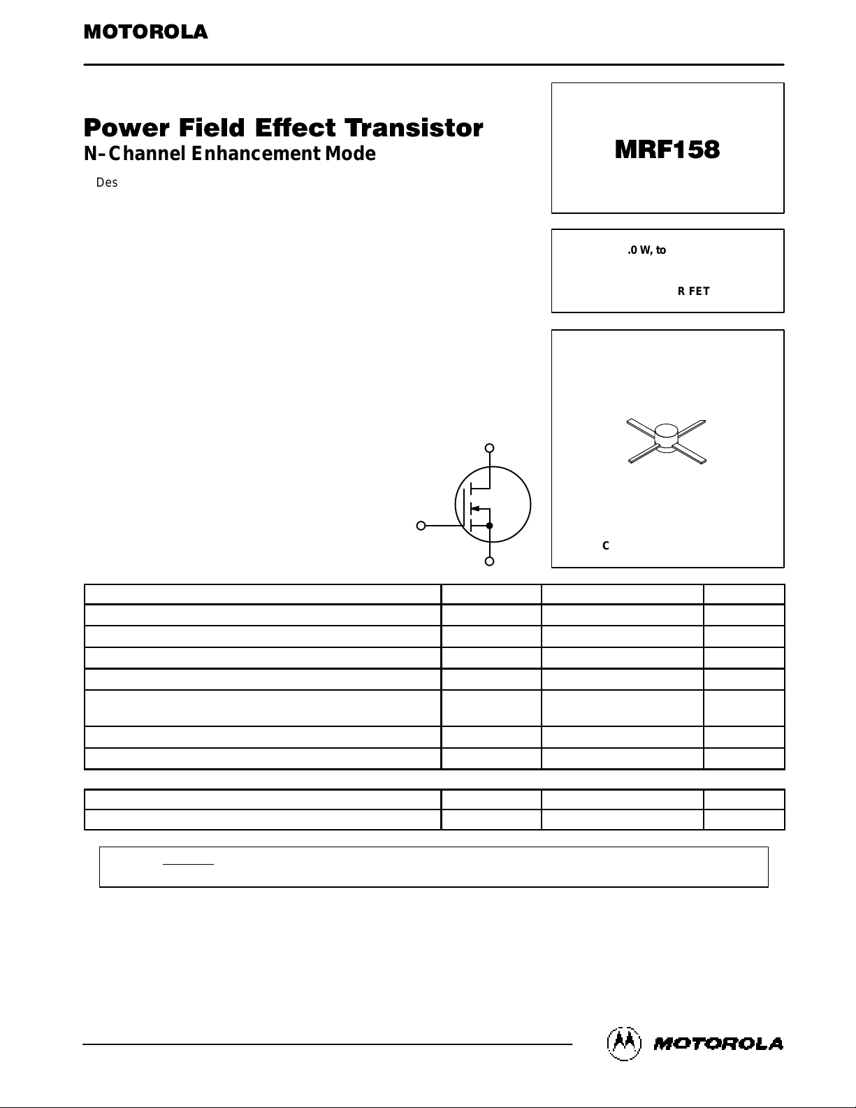
N–Channel Enhancement Mode
Designed for wideband large–signal amplifier and oscillator applications to
500 MHz.
• Guaranteed 28 Volt, 400 MHz Performance
Output Power = 2.0 Watts
Minimum Gain = 16 dB
Efficiency = 55% (Typical)
• Grounded Source Package for High Gain and Excellent Heat
Dissipation (MRF158R)
• Facilitates Manual Gain Control, ALC and Modulation
Techniques
• 100% Tested for Load Mismatch at All Phase Angles with
30:1 VSWR
• Excellent Thermal Stability, Ideally Suited for Class A
Operation
• Circuit board photomaster available upon request by
contacting RF Tactical Marketing in Phoenix, AZ.
MAXIMUM RATINGS
Rating Symbol Value Unit
Drain–Source Voltage V
DSS
65 Vdc
Drain–Gate Voltage (RGS = 1.0 MΩ) V
DGR
65 Vdc
Gate–Source Voltage V
GS
±40 Vdc
Drain Current — Continuous I
D
0.5 Adc
Total Device Dissipation @ TC = 25°C
Derate above 25°C
P
D
8.0
45
Watts
mW/°C
Storage Temperature Range T
stg
–65 to +150 °C
Operating Junction Temperature T
J
200 °C
THERMAL CHARACTERISTICS
Characteristic Symbol Max Unit
Thermal Resistance, Junction to Case R
θJC
13.2 °C/W
NOTE — CAUTION — MOS devices are susceptible to damage from electrostatic charge. Reasonable precautions in handling and
packaging MOS devices should be observed.
Order this document
by MRF158/D
SEMICONDUCTOR TECHNICAL DATA
2.0 W, to 500 MHz
TMOS
BROADBAND
RF POWER FET
CASE 305A–01, STYLE 2
Motorola, Inc. 1994
D
S
G
REV 6
MRF158
2
MOTOROLA RF DEVICE DATA
ELECTRICAL CHARACTERISTICS (T
C
= 25°C unless otherwise noted.)
Characteristic
Symbol Min Typ Max Unit
OFF CHARACTERISTICS
Drain–Source Breakdown Voltage (VGS = 0, ID = 5.0 mA) V
(BR)DSS
65 — — Vdc
Zero Gate Voltage Drain Current (VDS = 28 V, VGS = 0) I
DSS
— — 0.5 mAdc
Gate–Source Leakage Current (VGS = 40 V, VDS = 0) I
GSS
— — 1.0 µAdc
ON CHARACTERISTICS
Gate Threshold Voltage (ID = 10 mA, VDS = 10 V) V
GS(th)
1.0 4.0 6.0 Vdc
Forward Transconductance (VDS = 10 V, ID = 100 mA) g
fs
50 85 — mmhos
DYNAMIC CHARACTERISTICS
Input Capacitance (VDS = 28 V, VGS = 0, f = 1.0 MHz) C
iss
— 3.0 — pF
Output Capacitance (VDS = 28 V, VGS = 0, f = 1.0 MHz) C
oss
— 4.2 — pF
Reverse Transfer Capacitance (VDS = 28 V, VGS = 0, f = 1.0 MHz) C
rss
— 0.45 — pF
FUNCTIONAL CHARACTERISTICS (Figure 1)
Common Source Power Gain
(VDD = 28 Vdc, P
out
= 2.0 W, f = 400 MHz, IDQ = 100 mA)
G
ps
16 20 — dB
Drain Efficiency (Figure 1)
(VDD = 28 Vdc, P
out
= 2.0 W, f = 400 MHz, IDQ = 100 mA)
η 45 55 — %
Electrical Ruggedness (Figure 1)
(VDD = 28 Vdc, P
out
= 2.0 W, f = 400 MHz, IDQ = 100 mA,
VSWR 30:1 at all Phase Angles)
ψ
No Degradation in Output Power
Series Equivalent Input Impedance
(VDD = 28 V, P
out
= 2.0 W, f = 400 MHz, IDQ = 100 mA)
Z
in
— 8.8 – j27.37 — Ohms
Series Equivalent Output Impedance
(VDD = 28 V, P
out
= 2.0 W, f = 400 MHz, IDQ = 100 mA)
Z
out
— 16.96 – j62 — Ohms
 Loading...