

Motorola MRF151G Datasheet
SEMICONDUCTOR TECHNICAL DATA
The RF MOSFET Line
N–Channel Enhancement–Mode MOSFET
Designed for broadband commercial and military applications at frequencies
to 175 MHz. The high power, high gain and broadband performance of this
device makes possible solid state transmitters for FM broadcast or TV channel
frequency bands.
• Guaranteed Performance at 175 MHz, 50 V:
Output Power — 300 W
Gain — 14 dB (16 dB Typ)
Efficiency — 50%
• Low Thermal Resistance — 0.35°C/W
• Ruggedness Tested at Rated Output Power
• Nitride Passivated Die for Enhanced Reliability
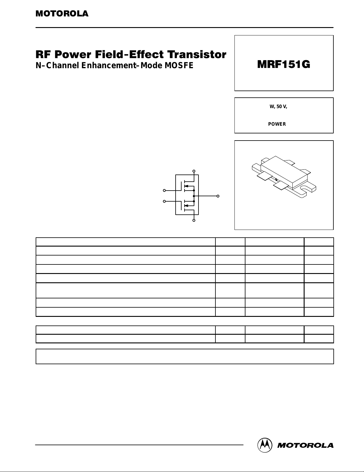
D
Order this document
by MRF151G/D
300 W, 50 V, 175 MHz
N–CHANNEL
BROADBAND
RF POWER MOSFET
G
G
D
S
(FLANGE)
CASE 375–04, STYLE 2
MAXIMUM RATINGS
Rating Symbol Value Unit
Drain–Source Voltage V
Drain–Gate Voltage V
Gate–Source Voltage V
Drain Current — Continuous I
Total Device Dissipation @ TC = 25°C
Derate above 25°C
Storage Temperature Range T
Operating Junction Temperature T
DSS
DGO
GS
D
P
D
stg
J
125 Vdc
125 Vdc
±40 Vdc
40 Adc
500
2.85
–65 to +150 °C
200 °C
THERMAL CHARACTERISTICS
Characteristic Symbol Max Unit
Thermal Resistance, Junction to Case R
NOTE — CAUTION — MOS devices are susceptible to damage from electrostatic charge. Reasonable precautions in handling and
packaging MOS devices should be observed.
θJC
0.35 °C/W
Watts
W/°C
REV 8
Motorola, Inc. 1997
MRF151GMOTOROLA RF DEVICE DATA
1
ELECTRICAL CHARACTERISTICS (T
Characteristic Symbol Min Typ Max Unit
= 25°C unless otherwise noted.)
C
OFF CHARACTERISTICS (Each Side)
Drain–Source Breakdown Voltage (VGS = 0, ID = 100 mA) V
Zero Gate Voltage Drain Current (VDS = 50 V, VGS = 0) I
Gate–Body Leakage Current (VGS = 20 V, VDS = 0) I
ON CHARACTERISTICS (Each Side)
Gate Threshold Voltage (VDS = 10 V, ID = 100 mA) V
Drain–Source On–Voltage (VGS = 10 V, ID = 10 A) V
Forward Transconductance (VDS = 10 V, ID = 5.0 A) g
DYNAMIC CHARACTERISTICS (Each Side)
Input Capacitance (VDS = 50 V, VGS = 0, f = 1.0 MHz) C
Output Capacitance (VDS = 50 V, VGS = 0, f = 1.0 MHz) C
Reverse Transfer Capacitance (VDS = 50 V, VGS = 0, f = 1.0 MHz) C
FUNCTIONAL TESTS
Common Source Amplifier Power Gain
(VDD = 50 V, P
Drain Efficiency
(VDD = 50 V, P
Load Mismatch
(VDD = 50 V, P
VSWR 5:1 at all Phase Angles)
= 300 W, IDQ = 500 mA, f = 175 MHz)
out
= 300 W, f = 175 MHz, ID (Max) = 11 A)
out
= 300 W, IDQ = 500 mA,
out
(BR)DSS
DSS
GSS
GS(th)
DS(on)
fs
iss
oss
rss
G
ps
η 50 55 — %
ψ
125 — — Vdc
— — 5.0 mAdc
— — 1.0 µAdc
1.0 3.0 5.0 Vdc
1.0 3.0 5.0 Vdc
5.0 7.0 — mhos
— 350 — pF
— 220 — pF
— 15 — pF
14 16 — dB
No Degradation in Output Power
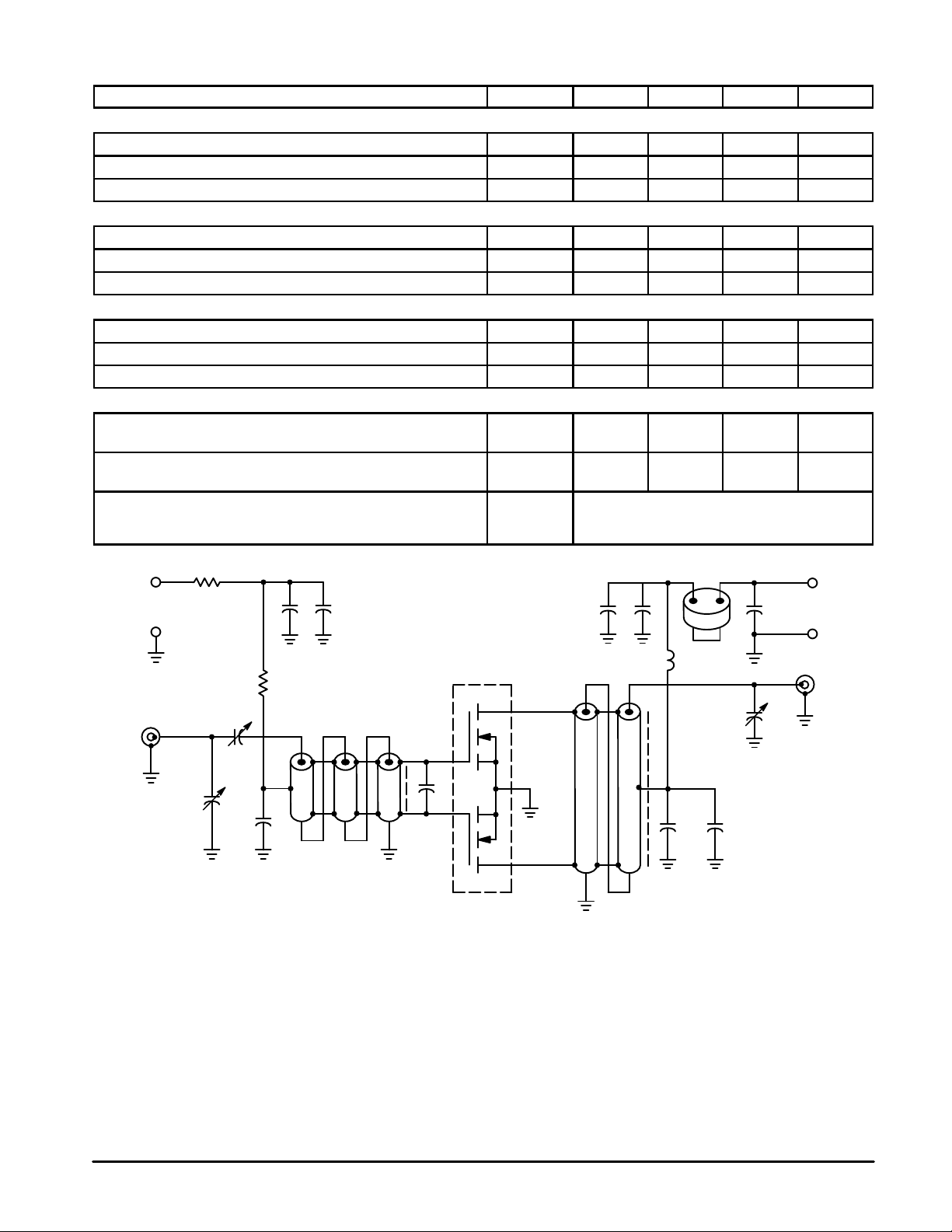
C2
R1
C1
C1
C5C4
R2
T1
C6
C3
+
BIAS 0–6 V
–
INPUT
R1 — 100 Ohms, 1/2 W
R2 — 1.0 kOhm, 1/2 W
C1 — Arco 424
C2 — Arco 404
C3, C4, C7, C8, C9 — 1000 pF Chip
C5, C10 — 0.1 µF Chip
C6 — 330 pF Chip
C11 — 0.47 µF Ceramic Chip, Kemet 1215 or
C11 — Equivalent (100 V)
C12 — Arco 422
L1 — 10 Turns AWG #18 Enameled Wire,
L1 — Close Wound, 1/4″ I.D.
L2 — Ferrite Beads of Suitable Material for
L2 — 1.5–2.0 µH Total Inductance
Unless Otherwise Noted, All Chip Capacitors are ATC Type 100 or
Equivalent.
Figure 1. 175 MHz Test Circuit
L2
C10C9
D.U.T.
T1 — 9:1 RF Transformer. Can be made of 15–18 Ohms
T1 — Semirigid Co–Ax, 62–90 Mils O.D.
T2 — 1:4 RF Transformer. Can be made of 16–18 Ohms
T2 — Semirigid Co–Ax, 70–90 Mils O.D.
Board Material — 0.062″ Fiberglass (G10),
1 oz. Copper Clad, 2 Sides, εr = 5.0
NOTE: For stability, the input transformer T1 must be loaded
NOTE: with ferrite toroids or beads to increase the common
NOTE: mode inductance. For operation below 100 MHz. The
NOTE: same is required for the output transformer.
See Figure 6 for construction details of T1 and T2.
T2
L1
C7 C8
C11
C12
+
50 V
–
OUTPUT
MRF151G
2
MOTOROLA RF DEVICE DATA
 Loading...