

Motorola MPC931FA, MPC930FA Datasheet
SEMICONDUCTOR TECHNICAL DATA
1
REV 3
Motorola, Inc. 1997
1/97
The MPC930/931 is a 3.3V compatible, PLL based clock driver device
targeted for high performance clock applications. With output frequencies
of up to 150MHz and output skews of 300ps the MPC930/931 is ideal for
the most demanding clock distribution designs. The device employs a
fully differential PLL design to minimize cycle to cycle and long term jitter.
This parameter is of significant importance when the clock driver is
providing the reference clock for PLL’ s on board todays microprocessors
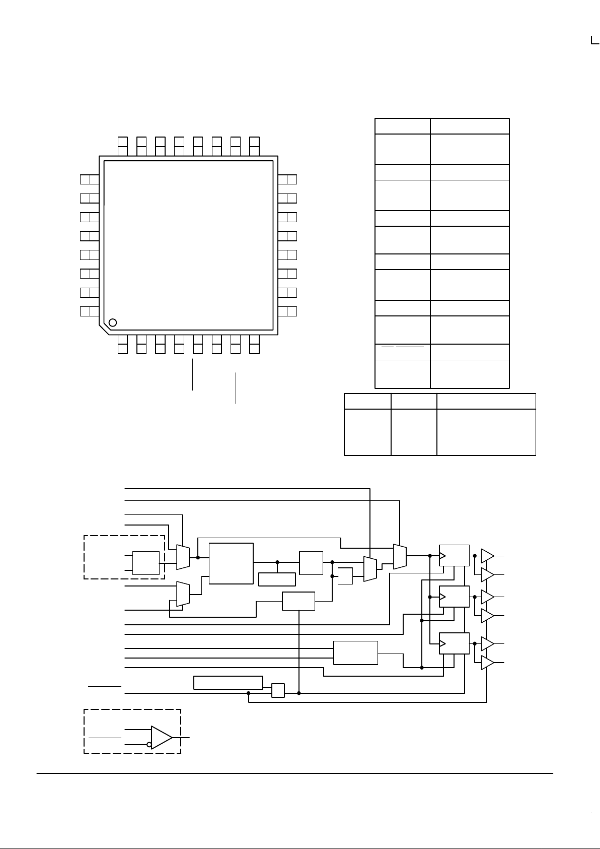
and ASiC’s. The device offers 6 low skew outputs, and a choice between
internal or external feedback. The feedback option adds to the flexibility of
the device, providing numerous input to output frequency relationships.
• On–Board Crystal Oscillator (MPC930)
• Differential LVPECL Reference Input (MPC931)
• Fully Integrated PLL
• Output Shut Down Mode
• Output Frequency up to 150MHz
• Compatible with PowerPC and Intel Microprocessors
• 32–Lead TQFP Packaging
• Power Down Mode
• ±100ps Typical Cycle–to–Cycle Jitter
The MPC930 and MPC931 are very similar in basic functionality, but
there are some minor differences. The MPC931 has been optimized for
use as a zero delay buffer . In addition to tighter specification limits on the
phase offset of the device, a higher speed VCO has been used on the
MPC931. The MPC930, on the other hand, is more optimized for use as a
clock generator. When choosing between the 930 and 931, pay special
attention to the differences in the AC parameters of each device.
The MPC930/931 offers two power saving features for power conscious portable or “green” designs. The power down pin will
seemlessly reduce all of the clock rates by one half so that the system will run at half the potential clock rate to extend battery life.
The POWER_DN pin is synchronized internally to the slowest output clock rate. This allows the transition in and out of the
power–down mode to be output glitch free. In addition, the shut down control pins will turn off various combinations of clock
outputs while leaving a subset active to allow for total processor shut down while maintaining system monitors to “wake up” the
system when signaled. During shut down, the PLL will remain locked, if internal feedback is used, so that wake up time will be
minimized. The shut down and power down pins can be combined for the ultimate in power savings. The Shut_Dn pins are
synchronized to the clock internal to the chip to eliminate the possibility of generating runt pulses.
The MPC930/931 devices offer a great deal of flexibility in what is used as the PLL reference. The MPC930 offers an
integrated crystal oscillator that allows for an inexpensive crystal to be used as the frequency reference. For more information on
the crystal oscillator please refer to the applications section of this data sheet. In those applications where the 930/931 will be
used to regenerate clocks from an existing source or as a zero delay buffer , alternative reference clock inputs are provided. Both
devices offer an LVCMOS input that can be used as the PLL reference. In addition the MPC931 replaces the crystal oscillator
inputs with a differential PECL reference clock input that allows the device to be used in mixed technology clock distribution trees.
An internal feedback divide by 8 of the VCO frequency is compared with the input reference provided by the on–board crystal
oscillator when the internal feedback is selected. The on–board crystal oscillator requires no external components other than a
series resonant crystal (see Applications Information section for more on crystals). The internal VCO is running at 8x the input
reference clock. The outputs can be configured to run at 4x, 2x, 1.25x or 0.66x the input reference frequency. If the external
feedback is selected, one of the MPC931’s outputs must be connected to the Ext_FB pin. Using the external feedback, numerous
input/output frequency relationships can be developed.
The MPC930/931 is fully 3.3V compatible and requires no external loop filter components. All control inputs accept LVCMOS
or LVTTL compatible levels while the outputs provide LVCMOS levels with the capability to drive terminated 50Ω transmission
lines. For series terminated applications, each output can drive two 50Ω transmission lines, effectively increasing the fanout to
1:12. The device is packaged in a 32–lead TQFP package to provide the optimum combination of board density and cost.
PowerPC is a trademark of International Business Machines Corporation. Pentium is a trademark of Intel Corporation.
LOW VOLTAGE
PLL CLOCK DRIVER
FA SUFFIX
32–LEAD TQFP PACKAGE
CASE 873A–02
MPC930 MPC931
MOTOROLA TIMING SOLUTIONS
BR1333 — Rev 6
2
÷2÷4÷2÷4÷4
÷6
FUNCTION TABLES
TCLK_Sel Reference
0
1
xtal (PECL_CLK)
TCLK
PLL_En PLL Status
0
1
Test Mode
PLL Enabled
ExtFB_Sel Reference
0
1
Int. ÷8
Ext_FB
GNDO
Qa1
Qa0
VCCO
Div_Sela
Div_Selb
Div_Selc
NC
GNDO
Qc1
Qc0
VCCO
Ext_FB
Shut_Dn1
Shut_Dn0
NC
GNDO
Qb0
Qb1
VCCO
ExtFB_Sel
TCLK_Sel
PLL_En
NC
NC
PLL_VCC
Power_Dn
TCLK
MR/Tristate
xtal1 (930)
xtal2 (930)
GNDI
25
26
27
28
29
30
31
32
15
14
13
12
11
10
9
12345678
24 23 22 21 20 19 18 17
16
MPC930/
MPC931
Power_Dn PLL Status
0
1
VCO/1
VCO/2
Div_Sela,b,c
0
1
Qa Qb Qc
Shut_Dn1
0
0
1
1
Div_Seln
Qb & Qc Low, Qa Toggle
Qa & Qb Low, Qc Toggle
Qb Low, Qa & Qc Toggle
All Toggle
Shut_Dn0
0
1
0
1
Figure 1. 32–Lead Pinout (Top View)
PECL_CLK (931)
PECL_CLK (931)
Figure 2. Logic Diagram
POWER–ON RESET
VCO
PHASE
DETECTOR
LPF
÷
8
MR/Tristate
xtal
OSC
Shut_Dn1
Shut_Dn0
xtal2
xtal1
PLL_En
Qa0
Qb0
Qb1
Power_Dn
÷2/÷
4
÷2/÷
4
÷4/÷
6
Qc0
Qc1
DISABLE
LOGIC
Div_Selb
Div_Sela
Qa1
TCLK
TCLK_Sel
Ext_FB
ExtFB_Sel
Div_Selc
MPC930
PECL_CLK
PECL_CLK
MPC931
MR/Tristate PLL Status
0
1
Disabled
Enabled
(Pullup)
(Pullup)
(Pulldown)
(Pullup)
(Pullup)
(Pulldown)
(Pulldown)
(Pulldown)
(Pullup)
(Pullup)
(Pulldown)
(Pullup)
(Pullup)
(None)
÷
2
MPC930 MPC931
TIMING SOLUTIONS
BR1333 — Rev 6
3 MOTOROLA
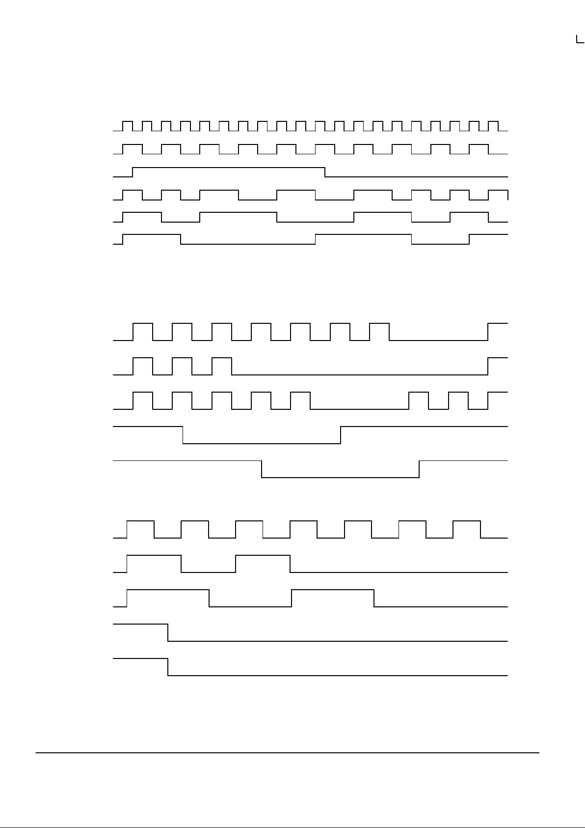
Figure 3. Power_Dn Timing Diagram
VCO
Figure 4. Shut_Dn Timing Diagram
Qa
Qb
Qc
SHUT_DN0
SHUT_DN1
Qa (÷2)
Qb (÷4)
Qc (
÷
6)
SHUT_DN0
SHUT_DN1
VCO/2
Power_Dn
Qa (÷2)
Qb (÷4)
Qc (÷6)
MPC930 MPC931
MOTOROLA TIMING SOLUTIONS
BR1333 — Rev 6
4
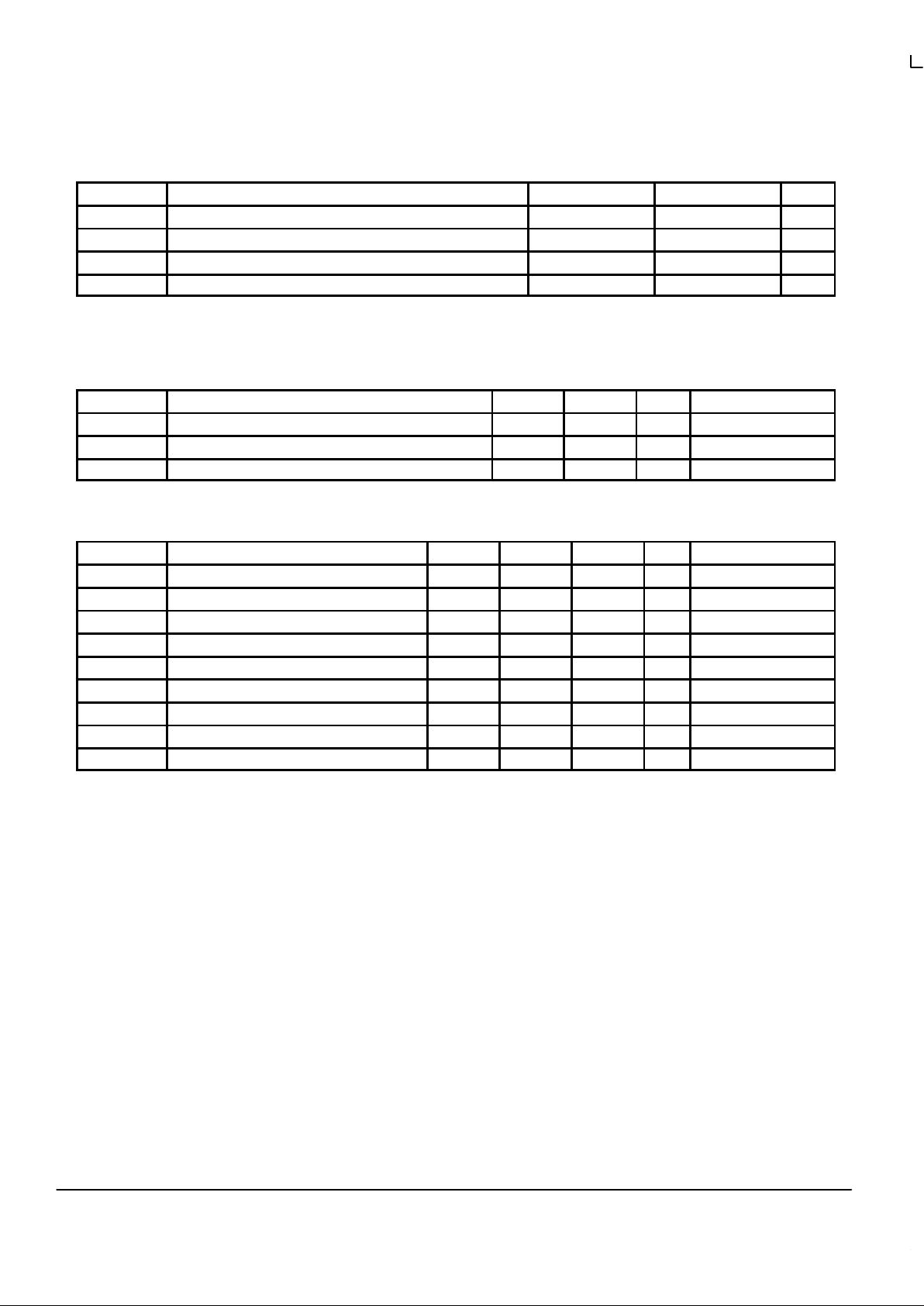
ABSOLUTE MAXIMUM RATINGS*
Symbol Parameter Min Max Unit
V
CC
Supply Voltage –0.3 4.6 V
V
I
Input Voltage –0.3 VDD + 0.3 V
I
IN
Input Current ±20 mA
T
Stor
Storage Temperature Range –40 125 °C
* Absolute maximum continuous ratings are those values beyond which damage to the device may occur. Exposure to these conditions or
conditions beyond those indicated may adversely affect device reliability. Functional operation under absolute–maximum–rated conditions is
not implied.
PLL INPUT REFERENCE CHARACTERISTICS (TA = 0 to 70°C)
Symbol Characteristic Min Max Unit Condition
tr, t
f
TCLK Input Rise/Falls 3.0 ns
f
ref
Reference Input Frequency 10 Note 1. MHz
f
refDC
Reference Input Duty Cycle 25 75 %
1. Maximum input reference frequency is limited by the VCO lock range and the feedback divider.
DC CHARACTERISTICS (TA = 0° to 70°C, VCC = 3.3V ±5%)
Symbol Characteristic Min Typ Max Unit Condition
V
IH
Input HIGH Voltage 2.0 3.6 V
V
IL
Input LOW Voltage 0.8 V
V
OH
Output HIGH Voltage 2.4 V IOH = –20mA (Note 2.)
V
OL
Output LOW Voltage 0.5 V IOL = 20mA (Note 2.)
I
IN
Input Current ±120 µA Note 3.
I
CC
Maximum Core Supply Current 65 85 mA
I
CCPLL
Maximum PLL Supply Current 15 20 mA
C
IN
4 pF
C
pd
25 pF Per Output
2. The MPC930/931 outputs can drive series or parallel terminated 50Ω (or 50Ω to VCC/2) transmission lines on the incident edge (see Applications
Info section).
3. Inputs have pull–up/pull–down resistors which affect input current.
MPC930 MPC931
TIMING SOLUTIONS
BR1333 — Rev 6
5 MOTOROLA
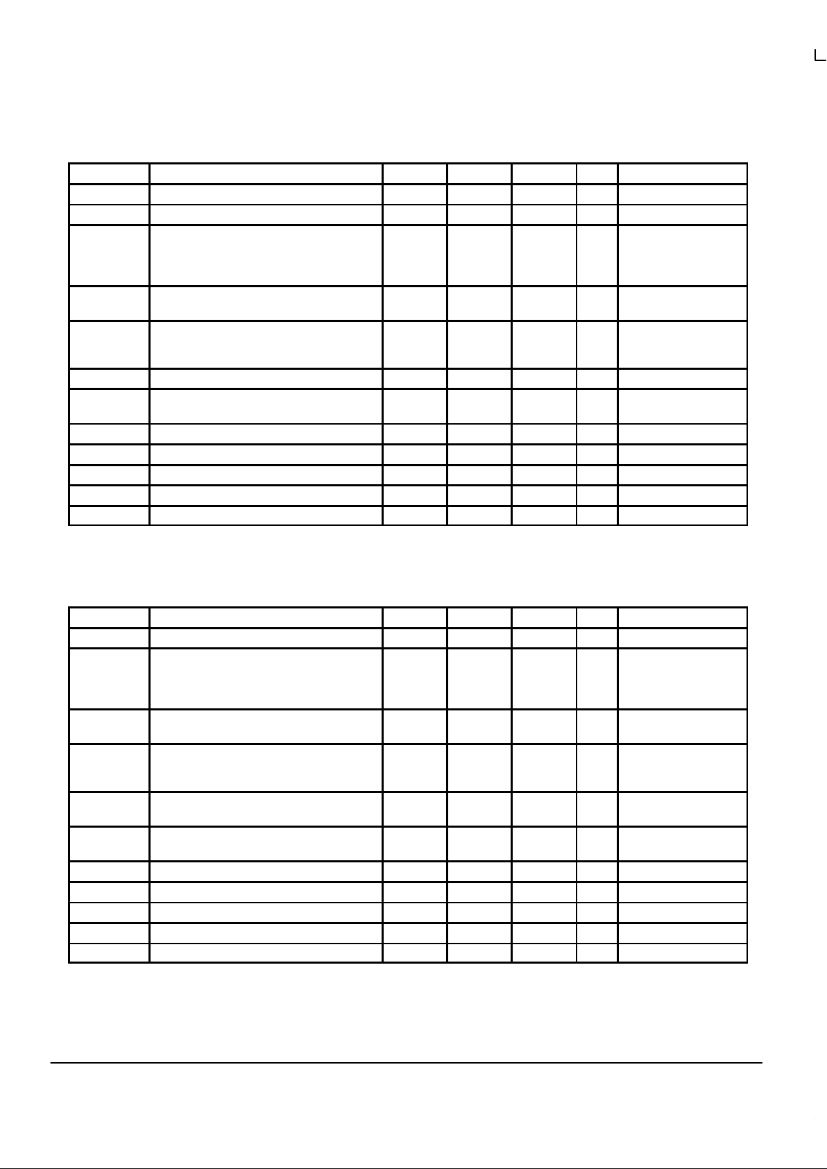
MPC930 AC CHARACTERISTICS (TA = 0° to 70°C, VCC = 3.3V ±5%)
Symbol Characteristic Min Typ Max Unit Condition
f
xtal
Crystal Oscillator Frequency Range 10 20 MHz Note 5., Note 7.
f
ref
Input Reference Frequency Note 7. Note 7. MHz Ref = TCLK
t
os
Output–to–Output Skew Same Frequency
(Note 4.) Diff Frequency
Same Frequency
Diff Frequency
200
300
300
450
300
400
400
600
ps f
max
≤ 100MHz
f
max
≤ 100MHz
f
max
> 100MHz
f
max
> 100MHz
f
VCO
VCO Lock Range Power_Dn = 0
Power_Dn = 1
100
50
280
140
MHz
f
max
Maximum Output Frequency Qa, Qb (÷2)
Qa, Qb, Qc (÷4)
Qc (÷6)
140
80
47
MHz Note 4.
t
pd
TCLK to EXT_FB Delay –600 –100 400 ps f
ref
= 50MHz, FB = ÷4
t
pw
Output Duty Cycle (Note 4.) t
CYCLE
/2
–750
t
CYCLE
/2
±500
t
CYCLE
/2
+750
ps
tr, t
f
Output Rise/Fall Time (Note 4.) 0.1 1.0 ns 0.8 to 2.0V
t
PLZ
, t
PHZ
Output Disable Time 2.0 8.0 ns 50Ω to VCC/2
t
PZL
Output Enable Time 2.0 10 ns 50Ω to VCC/2
t
jitter
Cycle–to–Cycle Jitter (Peak–to–Peak) ±100 ps Note 6.
t
lock
Maximum PLL Lock Time 10 ms
4. Measured with 50Ω to VCC/2 termination.
5. See Applications Info section for more Crystal specifications.
6. See Applications Info section for more jitter information.
7. Input reference frequency is bounded by VCO lock range and feedback divide selection.
MPC931 AC CHARACTERISTICS (TA = 0° to 70°C, VCC = 3.3V ±5%)
Symbol Characteristic Min Typ Max Unit Condition
f
ref
Input Reference Frequency Note 11. Note 11. MHz
t
os
Output–to–Output Skew Same Frequency
(Note 8.) Diff Frequency
Same Frequency
Diff Frequency
200
300
300
450
300
400
400
600
ps f
max
≤ 100MHz
f
max
≤ 100MHz
f
max
> 100MHz
f
max
> 100MHz
f
VCO
VCO Lock Range Power_Dn = 0
Power_Dn = 1
200
100
480
240
MHz
f
max
Maximum Output Frequency Qa, Qb (÷2)
Qa, Qb, Qc (÷4)
Qc (÷6)
150
120
80
MHz Note 9.
t
pd
Reference to EXT_FB Average Delay TCLK
PECL_CLK
–150
–400
0
–250
+150
–100
ps f
ref
= 50MHz; FB = ÷8;
Note 12.
t
pw
Output Duty Cycle (Note 8.) t
CYCLE
/2
–750
t
CYCLE
/2
±500
t
CYCLE
/2
+750
ps
tr, t
f
Output Rise/Fall Time (Note 8.) 0.1 1.0 ns 0.8 to 2.0V
t
PLZ
, t
PHZ
Output Disable Time 2.0 8.0 ns 50Ω to VCC/2
t
PZL
Output Enable Time 2.0 10 ns 50Ω to VCC/2
t
jitter
Cycle–to–Cycle Jitter (Peak–to–Peak) ±100 ps Note 10.
t
lock
Maximum PLL Lock Time 10 ms
8. Measured with 50Ω to VCC/2 termination.
9. f
max
limited by skew spec. Outputs will generate valid CMOS signals up to 180MHz.
10.See Applications Info section for more jitter information.
11.Input reference frequency is bounded by VCO lock range and feedback divide selection.
12.tpd is specified for 50MHz input reference, the window will shrink/grow proportionally from the minimum limit with shorter/linger reference
periods. The tpd does not include jitter.
 Loading...