

Page 1

PowerPC
™
MPC823e
Reference Manual
The Microprocessor for Mobile Computing
Motorola reserves the right to make changes without further notice to any products herein. Motorola makes no warranty, representation or guarantee regarding
the suitability of its products for any particular purpose, nor does Motorola assume any liability arising out of the application or use of any product or circuit, and
specifically disclaims any and all liability, including without limitation consequential or incidental damages. "Typical" parameters can and do vary in different
applications. All operating parameters, including "Typicals" must be validated for each customer application b y customer's technical experts. Motorola does not
convey any license under its patent rights nor the rights of others. Motorola products are not designed, intended, or authorized for use as components in
systems intended for surgical implant into the body , or other applications intended to support or sustain life, or f or any other application in which the f ailure of the
Motorola product could create a situation where personal injury or death may occur. Should Buy er purchase or use Motorola products f or any such unintended
or unauthorized application, Buyer shall indemnify and hold Motorola and its officers, employees, subsidiaries, affiliates, and distributors harmless against all
claims, costs, damages, and expenses, and reasonable attorney fees arising out of, directly or indirectly, any claim of personal injury or death associated with
such unintended or unauthorized use, even if such claim alleges that Motorola was negligent regarding the design or manuf acture of the part. Motorola and
are registered trademarks of Motorola, Inc. Motorola, Inc. is an Equal Opportunity/Affirmative Action Employ er.
©
2000 Motorola, Inc. All Rights Reserved. Revision 0
Page 2

Trademarks
™
QUICC
is a registered trademark of Motorola, Inc. PowerPC
and is used by Motorola under license from IBM. I
AppleTalk
®
is a trademark of Apple Computer, Inc.
™
2
is a registered trademark of IBM Corporation
®
C
is a registered tradmark of Philips Corporation.
All other trademarks are the property of their respective owners.
Acknowledgments
The MPC823e Support Team would like to thank the following people for their
Art Miller, CW Clark, Ken Edwards, Kevin Owen, Ray Burgess, Tom Gunter, John Round, Mike Shoemake,
James Wilson, Chris Lines, Ricardo Berger, Yehuda Rudin, Yair Liebman, Udi Barel, the rest of the Israel
design team, Stu Werbner, Tiffany Huling-Broadous, John Dailey, Lan Nguyen, Richard Hendricks,
Darcy Volden, Trish Sierer, Arnaldo Cruz, Danny Nguyen, Myle Buchanan, Joseph Mayfield, Rodolfo Guillen,
the rest of the product/test engineering team, Brian McCalley, Alan Weiss, Steve Rosebaugh, Jasmine Hsiao,
Mike Collier, John Southard, Joseph Lee, Pat Carr, Mark VandenBrink, the rest of the Systems Software team,
Yoichi Kimura, Yuzo Kuramochi, Tanamachi Goro, Fumihiko Kondo, Keiji Momozaki, Jean-Paul Davi,
Per-Eric Josefsson, Rodney Watt, Axel Streicher, Pierre Juste, Gary Segal, Mark DiPerri, Kurt Miller,
Steve Shoap, Rob Wackerman, Rick Heider, Gary Wilson, Thomas Yeh, Bill Durrenberger, Dave Hyder,
the rest of the Field Applications Engineering/Sales support team, Pamela Mitchell, Nina Friedman,
the rest of the Technical Information Center support team, Dan Malek, Jim Belesiu, Clark Liang, Ronny
Svensson, Mark Wagner, Bulent Egilmez, Kurt Fuqua, Robert Applebaum, Nick Vaccaro, Weifu Shi,
Roozbeh Ghorishi, Robert Ritchey, Brad Scott, Dan Malek, the rest of our customers,
the gang at comp.sys.powerpc.tech and linuxppc-embedded, and to many others.
contribution to the success of the MPC823e:
Page 3

TABLE OF CONTENTS
Paragraph Page
Number Title Number
Section 1
Introduction
1.1 Features ................................................................................................1-1
1.2 Architecture ...........................................................................................1-6
1.2.1 The Embedded PowerPC Core ..................................................1-8
1.2.2 The System Interface Unit ..........................................................1-8
1.2.3 The Communication Processor Module .....................................1-9
1.2.4 The Video/LCD Controller ........................................................1-10
1.2.4.1 The Video Controller .....................................................1-10
1.2.4.2 The LCD Controller .......................................................1-10
1.3 The PCMCIA-ATA Controller ..............................................................1-10
1.4 Power Management ............................................................................1-11
1.5 System Debug Support .......................................................................1-11
1.6 Applications .........................................................................................1-11
1.7 Differences Between MPC823 (Rev B) and MPC823e .......................1-12
1.8 MPC823e Glueless System Design ....................................................1-12
Section 2
External Signals
2.1 The System Bus Signals .......................................................................2-2
Section 3
Memory Map
Section 4
Reset
4.1 Types of Reset ......................................................................................4-2
4.1.1 Power-On Reset .........................................................................4-2
4.1.2 External Hard Reset ...................................................................4-3
4.1.3 Internal Hard Reset ....................................................................4-3
4.1.3.1 Loss of Lock ....................................................................4-3
4.1.3.2 Software Watchdog Reset ..............................................4-3
4.1.3.3 Checkstop Reset ............................................................4-3
4.1.3.4 Debug Port Hard Reset ..................................................4-4
4.1.3.5 JTAG Reset ....................................................................4-4
MOTOROLA
MPC823e REFERENCE MANUAL
i
Page 4

TABLE OF CONTENTS (Continued)
Paragraph Page
Number Title Number
4.1.4 External Soft Reset ....................................................................4-4
4.1.5 Internal Soft Reset .....................................................................4-4
4.1.5.1 Debug Port Soft Reset ....................................................4-4
4.2 Reset Status Register ...........................................................................4-5
4.3 How to Configure Reset ........................................................................4-7
4.3.1 Hard Reset .................................................................................4-7
4.3.1.1 Hard Reset Configuration Word ...................................4-10
4.3.2 Soft Reset ................................................................................4-12
Section 5
Clocks and Power Control
5.1 Features ................................................................................................5-1
5.2 Register Model ......................................................................................5-3
5.2.1 System Clock and Reset Control Register .................................5-3
5.2.2 PLL, Low-Power, and Reset Control Register ...........................5-7
5.3 The Clock Module ...............................................................................5-10
5.3.1 On-Chip Oscillators and External Clock Input ..........................5-12
5.3.2 System PLL ..............................................................................5-12
5.3.2.1 SPLL Stability ...............................................................5-13
5.3.3 The Low-Power Clock Divider ..................................................5-14
5.3.4 Internal Clock Signals ..............................................................5-16
5.3.4.1 The General System Clocks .........................................5-16
5.3.4.2 The Baud Rate Generator Clock ..................................5-19
5.3.4.3 The Synchronization Clocks .........................................5-20
5.3.4.4 The LCD Clocks ...........................................................5-21
5.3.5 Clock Configuration ..................................................................5-22
5.3.5.1 Mode Clock Pins ...........................................................5-22
5.3.5.2 The System Phase-Locked Loop Pins .........................5-23
5.4 Power Control .....................................................................................5-24
5.4.1 Power Rails ..............................................................................5-24
5.4.2 Keep-Alive Power .....................................................................5-25
5.4.2.1 Power Switching Example ............................................5-26
5.4.2.2 Register Lock ................................................................5-27
5.5 Low-Power Operation .........................................................................5-28
Section 6
The PowerPC Core
6.1 Features ................................................................................................6-1
6.2 Basic Structure of the Core ...................................................................6-2
6.2.1 Instruction Flow Within the Core ................................................6-2
ii
MPC823e REFERENCE MANUAL
MOTOROLA
Page 5

TABLE OF CONTENTS (Continued)
Paragraph Page
Number Title Number
6.2.2 Basic Instruction Pipeline ...........................................................6-4
6.3 Sequencer Unit .....................................................................................6-4
6.3.1 Flow Control ...............................................................................6-5
6.3.2 Issuing Instructions .....................................................................6-6
6.3.3 Interrupts ....................................................................................6-7
6.3.4 Implementing the Precise Exception Model ...............................6-8
6.3.4.1 Restartability After An Interrupt .....................................6-10
6.3.5 Processing an Interrupt ............................................................6-11
6.3.6 Serialization ..............................................................................6-12
6.3.6.1 Latency .........................................................................6-12
6.3.7 The External Interrupt ...............................................................6-13
6.3.7.1 Latency .........................................................................6-13
6.3.8 Interrupt Ordering .....................................................................6-14
6.4 The Register Unit ................................................................................6-15
6.4.1 Control Registers ......................................................................6-16
6.4.1.1 Physical Location of Special Registers .........................6-19
6.4.1.2 PowerPC Standard Control Register Bit Assignment....6-20
6.4.1.2.1 Machine State Register ....................................6-20
6.4.1.2.2 The Condition Register ....................................6-22
6.4.1.2.3 Fixed-Point Exception Cause Register ............6-23
6.4.1.3 Initializing the Control Registers ...................................6-24
6.4.1.3.1 System Reset Interrupt ....................................6-24
6.4.1.3.2 Hard/Soft Reset ................................................6-24
6.5 The Fixed-Point Unit ...........................................................................6-24
6.5.1 XER Update In Divide Instructions ...........................................6-24
6.6 The Load/Store Unit ............................................................................6-25
6.6.1 Issuing Load/Store Instructions ................................................6-26
6.6.2 Serializing Load/Store Instructions ...........................................6-27
6.6.3 Instructions Issued to the Data Cache .....................................6-27
6.6.4 Issuing Store Instruction Cycles ...............................................6-27
6.6.5 Issuing Nonspeculative Load Instructions ................................6-27
6.6.6 Executing Unaligned Instructions .............................................6-28
6.6.7 Little-Endian Mode Support ......................................................6-29
6.6.8 Atomic Update Primitives .........................................................6-29
6.6.9 Instruction Timing .....................................................................6-30
6.6.10 Stalling Storage Control Instructions ........................................6-30
6.6.11 Accessing Off-Core Special Registers .....................................6-30
6.6.12 Storage Control Instructions .....................................................6-31
6.6.13 Exceptions ................................................................................6-31
6.6.13.1 DAR, DSISR, and BAR Operation ................................6-31
MOTOROLA
Section 7
MPC823e REFERENCE MANUAL
iii
Page 6

TABLE OF CONTENTS (Continued)
Paragraph Page
Number Title Number
PowerPC Architecture Compliance
7.1 PowerPC User Instruction Set Architecture (Book I) ............................7-1
7.1.1 Computation Modes ...................................................................7-1
7.1.2 Reserved Fields .........................................................................7-1
7.1.3 Classes of Instructions ...............................................................7-1
7.1.4 Exceptions ..................................................................................7-2
7.1.5 The Branch Processor ...............................................................7-2
7.1.6 Fetching Instructions ..................................................................7-2
7.1.7 Branch Instructions ....................................................................7-2
7.1.7.1 Invalid Branch Instruction Forms ....................................7-2
7.1.7.2 Branch Prediction ...........................................................7-2
7.1.8 The Fixed-Point Processor .........................................................7-2
7.1.8.1 Move To/From System Register Instructions .................7-3
7.1.8.2 Fixed-Point Arithmetic Instructions .................................7-3
7.1.9 The Load/Store Processor .........................................................7-3
7.1.9.1 Fixed-Point Load With Update and Store
With Update Instructions ................................................7-3
7.1.9.2 Fixed-Point Load and Store Multiple Instructions ...........7-3
7.1.9.3 Fixed-Point Load String Instructions ...............................7-3
7.1.9.4 Storage Synchronization Instructions .............................7-4
7.1.9.5 Optional Instructions .......................................................7-4
7.1.9.6 Little-Endian Byte Ordering ............................................7-4
7.2 PowerPC Virtual Environment Architecture (Book II) ............................7-4
7.2.1 Storage Model ............................................................................7-4
7.2.1.1 Memory Coherence ........................................................7-4
7.2.1.2 Atomic Update Primitives ...............................................7-4
7.2.2 The Effect Of Operand Placement on Performance ..................7-5
7.2.3 The Storage Control Instructions ...............................................7-5
7.2.4 Timebase ...................................................................................7-6
7.3 PowerPC Operating Environment Architecture (Book III) .....................7-6
7.3.1 The Branch Processor ...............................................................7-6
7.3.1.1 Machine State Register ..................................................7-6
7.3.1.2 Processor Version Register ............................................7-6
7.3.1.3 Branch Processors Instructions ......................................7-6
7.3.2 The Fixed-Point Processor .........................................................7-6
7.3.2.1 Unsupported Registers ...................................................7-6
7.3.2.2 Added Registers .............................................................7-6
7.3.3 Storage Model ............................................................................7-6
7.3.3.1 Address Translation ........................................................7-6
7.3.4 Reference and Change Bits .......................................................7-7
7.3.5 Storage Protection .....................................................................7-7
7.3.6 Storage Control Instructions .......................................................7-7
iv
MPC823e REFERENCE MANUAL
MOTOROLA
Page 7

TABLE OF CONTENTS (Continued)
Paragraph Page
Number Title Number
7.3.6.1 Data Cache Block Invalidate (dcbi) .................................7-7
7.3.6.2 TLB Invalidate Entry (tlbie) .............................................7-7
7.3.6.3 TLB Invalidate All (tlbia) ..................................................7-7
7.3.6.4 TLB Synchronize (tlbsync) ..............................................7-7
7.3.7 Interrupts ....................................................................................7-7
7.3.7.1 Classes ...........................................................................7-7
7.3.7.2 Processing ......................................................................7-8
7.3.7.3 Definitions .......................................................................7-8
7.3.7.3.1 System Reset Interrupt ......................................7-9
7.3.7.3.2 Machine Check Interrupt ....................................7-9
7.3.7.3.3 Data Storage Interrupt ......................................7-10
7.3.7.3.4 Instruction Storage Interrupt .............................7-10
7.3.7.3.5 Alignment Interrupt ...........................................7-10
7.3.7.3.6 Program Interrupt .............................................7-11
7.3.7.3.7 Floating-Point Unavailable Interrupt .................7-11
7.3.7.3.8 Trace Interrupt ..................................................7-11
7.3.7.3.9 Floating-Point Assist Interrupt ..........................7-11
7.3.7.3.10 Implementation-Dependent Software
Emulation Interrupt ............................................7-12
7.3.7.3.11 Implementation-Specific Instruction TLB
Miss Interrupt ....................................................7-12
7.3.7.3.12 Implementation-Specific Instruction TLB
Error Interrupt ....................................................7-13
7.3.7.3.13 Implementation-Specific Data TLB Miss
Interrupt ............................................................. 7-14
7.3.7.3.14 Implementation-Specific Data TLB Error
Interrupt ............................................................. 7-14
7.3.7.3.15 Implementation-Specific Debug Register .........7-15
7.3.7.4 Partially Executed Instructions ......................................7-17
7.3.8 Timer Facilities .........................................................................7-17
7.3.9 Optional Facilities and Instructions ...........................................7-17
Section 8
Instruction Execution Timing
8.1 Instruction Timing List ...........................................................................8-1
8.2 Instruction Execution Timing Examples ................................................8-4
8.2.1 Data Cache Load .......................................................................8-4
8.2.2 Writeback ...................................................................................8-5
8.2.2.1 Writeback Arbitration ......................................................8-5
8.2.2.2 Private Writeback Bus Load ...........................................8-6
8.2.3 Fastest External Load (Data Cache Miss) ..................................8-7
MOTOROLA
MPC823e REFERENCE MANUAL
v
Page 8

TABLE OF CONTENTS (Continued)
Paragraph Page
Number Title Number
8.2.4 A Full History Buffer ...................................................................8-8
8.2.5 Branch Folding ...........................................................................8-9
8.2.6 Branch Prediction .....................................................................8-10
Section 9
Instruction Cache
9.1 Features ................................................................................................9-1
9.2 Programming the Instruction Cache .....................................................9-4
9.2.1 Instruction Cache Control and Status Register ..........................9-5
9.2.2 Instruction Cache Address Register ...........................................9-6
9.2.3 Instruction Cache Data Port Register .........................................9-7
9.3 Instruction Cache Operation .................................................................9-7
9.3.1 Instruction Cache Hit ..................................................................9-7
9.3.2 Instruction Cache Miss ...............................................................9-8
9.3.3 Instruction Fetch On A Predicted Path .......................................9-8
9.4 instruction Cache Commands ...............................................................9-8
9.4.1 Invalidating the Instruction Cache ..............................................9-9
9.4.2 Loading and Locking the Instruction Cache .............................9-10
9.4.3 Unlocking A Line ......................................................................9-10
9.4.4 Unlocking the Entire Instruction Cache ....................................9-11
9.4.5 Inhibiting the Instruction Cache ................................................9-11
9.4.6 Instruction Cache Read ............................................................9-12
9.4.7 Instruction Cache Write ............................................................9-14
9.5 Restrictions .........................................................................................9-14
9.6 Instruction Cache Coherency ..............................................................9-14
9.7 Updating Code And Memory Region Attributes ..................................9-14
9.8 Reset Sequence .................................................................................9-14
9.9 Debug Support ....................................................................................9-15
9.9.1 Fetching Instructions From The Development Port ..................9-15
Section 10
Data Cache
10.1 Features ..............................................................................................10-1
10.2 Organization of the Data Cache ..........................................................10-2
10.3 Programming the Data Cache ............................................................10-3
10.3.1 PowerPC Architecture Instructions ..........................................10-3
10.3.1.1 PowerPC User Instruction Set Architecture (Book I).....10-3
10.3.1.2 PowerPC Virtual Environment Architecture (Book II)....10-4
10.3.1.3 PowerPC Operating Environment Architecture
(Book III) .......................................................................10-4
vi
MPC823e REFERENCE MANUAL
MOTOROLA
Page 9

TABLE OF CONTENTS (Continued)
Paragraph Page
Number Title Number
10.3.2 Implementation-Specific Operations ........................................10-4
10.3.3 Special Registers of the Data Cache .......................................10-4
10.3.3.1 Data Cache Control and Status Register ......................10-5
10.3.3.2 Data Cache Address Register ......................................10-7
10.3.3.3 Reading the Cache Structures ......................................10-7
10.4 Operating the Data Cache ................................................................10-10
10.4.1 Data Cache Read ...................................................................10-10
10.4.2 Data Cache Write ...................................................................10-10
10.4.2.1 Copyback Mode ..........................................................10-11
10.4.2.2 Writethrough Mode .....................................................10-12
10.4.3 Data Cache Inhibited Accesses .............................................10-12
10.4.4 Data Cache Freeze ................................................................10-12
10.4.5 Data Cache Coherency ..........................................................10-13
10.5 Data Cache Commands ....................................................................10-13
10.5.1 Flushing and Invalidating the Cache ......................................10-13
10.5.2 Enabling and Disabling the Cache .........................................10-13
10.5.3 Locking and Unlocking the Cache ..........................................10-13
10.5.4 Data Cache Instructions .........................................................10-14
10.5.4.1 dcbi, dcbst, dcbf And dcbz Instructions ......................10-14
10.5.4.2 Touch ..........................................................................10-14
10.5.4.3 Storage Synchronization/Reservation ........................10-14
10.5.5 Data Cache Read ...................................................................10-14
Section 11
Memory Management Unit
11.1 Features ..............................................................................................11-1
11.2 Address Translation ............................................................................11-2
11.2.1 Translation Lookaside Buffer Operation ...................................11-2
11.3 Protection ............................................................................................11-3
11.4 Storage Control ...................................................................................11-4
11.5 Translation Table Structure .................................................................11-5
11.5.1 Level One Descriptor ................................................................11-9
11.5.2 Level Two Descriptor ..............................................................11-10
11.6 Programming the Memory Management Unit ...................................11-15
11.6.1 Control Registers ....................................................................11-16
11.6.1.1 MMU Instruction Control Register ...............................11-16
11.6.1.2 MMU Data Control Register ........................................11-17
11.6.1.3 MMU Current Address Space ID Register ..................11-18
11.6.1.4 MMU Instruction Effective Page Number Register .....11-19
11.6.1.5 MMU Data Effective Page Number Register ..............11-20
11.6.1.6 MMU Instruction Real Page Number Register ............11-21
MOTOROLA
MPC823e REFERENCE MANUAL
vii
Page 10

TABLE OF CONTENTS (Continued)
Paragraph Page
Number Title Number
11.6.1.7 MMU Data Real Page Number Register ....................11-26
11.6.1.8 MMU Instruction Access Protection Register .............11-31
11.6.1.9 MMU Data Access Protection Register ......................11-32
11.6.1.10 MMU Instruction Tablewalk Control Register .............11-33
11.6.1.11 MMU Data Tablewalk Control Register ......................11-34
11.6.1.12 MMU Tablewalk Base Register ..................................11-36
11.6.1.13 MMU Tablewalk Special Register ...............................11-37
11.6.2 MMU Data Content-Addressable Registers ...........................11-37
11.6.2.1 MMU Data CAM Entry Read Register ........................11-38
11.6.2.2 MMU Data RAM Entry Read Register 0 .....................11-39
11.6.2.3 MMU Data RAM Entry Read Register 1 .....................11-41
11.6.3 MMU Instruction Content-Addressable Registers ..................11-43
11.6.3.1 MMU Instruction CAM Entry Read Register ...............11-43
11.6.3.2 MMU Instruction RAM Entry Read Register 0 ............11-45
11.6.3.3 MMU Instruction RAM Entry Read Register 1 ............11-46
11.7 Interrupts ...........................................................................................11-47
11.7.1 Implementation-Specific Instruction TLB Miss .......................11-47
11.7.2 Implementation-Specific Data TLB Miss ................................11-47
11.7.3 Implementation-Specific Instruction TLB Error .......................11-48
11.7.4 Implementation-Specific Data TLB Error ................................11-48
11.8 Manipulating the Translation Lookaside Buffer .................................11-49
11.8.1 Reloading the Translation Lookaside Buffer ..........................11-49
11.8.1.1 Translation Reload Examples .....................................11-50
11.8.2 Controlling the TLB Replacement Counter ............................11-51
11.8.3 Invalidating the Translation Lookaside Buffer ........................11-51
11.8.4 Loading the Reserved TLB Entries ........................................11-51
11.9 Requirements For Accessing The Memory Management Unit
Control Registers ..............................................................................11-52
Section 12
System Interface Unit
12.1 Features ..............................................................................................12-2
12.2 System Configuration and Protection .................................................12-2
12.3 Interrupt Configuration ........................................................................12-5
12.3.1 The Interrupt Structure .............................................................12-5
12.3.2 Priority of the Interrupt Sources ...............................................12-6
12.3.3 Programming the Interrupt Controller .......................................12-7
12.3.3.1 SIU Interrupt Pending Register .....................................12-7
12.3.3.2 SIU Interrupt Mask Register .........................................12-8
12.3.3.3 SIU Interrupt Edge/Level Register ................................12-9
12.3.3.4 SIU Interrupt Vector Register .....................................12-10
viii
MPC823e REFERENCE MANUAL
MOTOROLA
Page 11

TABLE OF CONTENTS (Continued)
Paragraph Page
Number Title Number
12.4 The Bus Monitor ................................................................................12-11
12.5 The PowerPC Decrementer ..............................................................12-12
12.5.1 Decrementer Register ............................................................12-13
12.6 The PowerPC Timebase ...................................................................12-14
12.6.1 Timebase Register .................................................................12-14
12.6.2 Timebase Reference Registers ..............................................12-15
12.6.3 Timebase Status and Control Register ..................................12-16
12.7 The Real-Time Clock ........................................................................12-17
12.7.1 Real-Time Clock Status and Control Register ........................12-18
12.7.2 Real-Time Clock Register ......................................................12-19
12.7.3 Real-Time Clock Alarm Seconds Register .............................12-20
12.7.4 Real-Time Clock Alarm Register ............................................12-21
12.8 The Periodic Interrupt Timer .............................................................12-22
12.8.1 Periodic Interrupt Status and Control Register .......................12-23
12.8.2 Periodic Interrupt Timer Count Register .................................12-24
12.8.3 Periodic Interrupt Timer Register ...........................................12-25
12.9 The Software Watchdog Timer .........................................................12-26
12.9.1 Software Service Register ......................................................12-27
12.10 Freeze Operation ..............................................................................12-28
12.10.1 Low-Power Stop Operation ....................................................12-28
12.11 Multiplexing the System Interface Unit Pins ......................................12-29
12.12 Programming the System Interface Unit ...........................................12-30
12.12.1 System Configuration and Protection Registers .....................12-30
12.12.1.1 SIU Module Configuration Register ............................12-30
12.12.1.2 Internal Memory Map Register ...................................12-34
12.12.1.3 System Protection Control Register ............................12-35
12.12.1.4 Transfer Error Status Register ....................................12-36
Section 13
External Bus Interface
13.1 Features ..............................................................................................13-1
13.2 Transfer Signals ..................................................................................13-1
13.2.1 Control Signals .........................................................................13-3
13.3 Bus Signal Descriptions ......................................................................13-4
13.4 Bus Interface Operation ......................................................................13-7
13.4.1 Basic Transfers ........................................................................13-8
13.4.2 Single Beat Transfers ...............................................................13-8
13.4.2.1 Single Beat Read Flow .................................................13-9
13.4.2.2 Single Beat Write Flow ...............................................13-12
13.4.3 Burst Transfers .......................................................................13-16
13.4.4 The Burst Mechanism ............................................................13-16
MOTOROLA
MPC823e REFERENCE MANUAL
ix
Page 12

x
TABLE OF CONTENTS (Continued)
Paragraph Page
Number Title Number
13.4.5 Transfer Alignment and Packaging ........................................13-25
13.4.6 Arbitration Phase-Related Signals .........................................13-27
13.4.6.1 Bus Request Signal ....................................................13-28
13.4.6.2 Bus Grant Signal ........................................................13-29
13.4.6.3 Bus Busy Signal .........................................................13-29
13.4.7 Address Transfer Phase-Related Signals ..............................13-31
13.4.7.1 Transfer Start Signal ...................................................13-31
13.4.7.2 Address Bus ...............................................................13-32
13.4.7.3 Transfer Attributes ......................................................13-32
13.4.7.3.1 Read/Write Signal ..........................................13-32
13.4.7.3.2 Burst Signal ....................................................13-32
13.4.7.3.3 Transfer Size Signal .......................................13-33
13.4.7.3.4 Address Space Attributes ..............................13-33
13.4.7.3.5 Special Transfer Start Signal .........................13-33
13.4.7.3.6 Burst Data in Progress Signal ........................13-36
13.4.8 Data Transfer Phase-Related Signals ....................................13-36
13.4.8.1 Data Signal .................................................................13-36
13.4.9 Termination Phase-Related Signals .......................................13-36
13.4.9.1 Transfer Acknowledge Signal .....................................13-36
13.4.9.2 Burst Inhibit Signal ......................................................13-36
13.4.9.3 Transfer Error Acknowledge Signal ............................13-36
13.4.9.4 Protocol for Termination Signals ................................13-37
13.4.10 Storage Reservation Protocol ................................................13-38
13.4.11 Exception Control Cycles .......................................................13-41
13.4.11.1 RETRY Signal ............................................................13-42
Section 14
Endian Modes
14.1 Little-Endian Features .........................................................................14-3
14.2 Big-Endian System Features ..............................................................14-5
14.3 PowerPC Little-Endian System Features ............................................14-5
14.4 Setting the Endian Mode Of Operation .............................................. 14-5
Section 15
Memory Controller
15.1 Features ..............................................................................................15-1
15.2 Architecture .........................................................................................15-4
15.3 Register Model ....................................................................................15-7
15.3.1 Register Descriptions ...............................................................15-9
15.3.1.1 Base Registers .............................................................15-9
MPC823e REFERENCE MANUAL
MOTOROLA
Page 13

TABLE OF CONTENTS (Continued)
Paragraph Page
Number Title Number
15.3.1.2 Option Registers .........................................................15-11
15.3.1.3 Memory Status Register .............................................15-15
15.3.1.4 Memory Command Register .......................................15-17
15.3.1.5 Machine A Mode Register ..........................................15-19
15.3.1.6 Machine B Mode Register ..........................................15-22
15.3.1.7 Memory Data Register ................................................15-26
15.3.1.8 Memory Address Register ..........................................15-26
15.3.1.9 Memory Periodic Timer Prescaler Register ................15-27
15.4 The General-Purpose Chip-Select Machine .....................................15-27
15.4.1 Configuration ..........................................................................15-27
15.4.1.1 Programmable Wait State Configuration ....................15-34
15.4.1.2 Extended Hold Time on Read Accesses ....................15-34
15.4.1.3 Boot Chip-Select Operation ........................................15-37
15.4.1.4 SRAM Interface ..........................................................15-38
15.4.1.5 External Asynchronous Master support ......................15-38
15.5 User-Programmable Machines .........................................................15-41
15.5.1 Requests ................................................................................15-42
15.5.1.1 Internal/External Memory Access Requests ...............15-43
15.5.1.2 Memory Periodic Timer Requests ..............................15-43
15.5.1.3 Software Requests .....................................................15-44
15.5.1.4 Exception Requests ....................................................15-44
15.5.2 Programming the User-Programmable Machine ....................15-44
15.5.3 Clock Timing ...........................................................................15-45
15.5.4 The RAM Array .......................................................................15-49
15.5.4.1 The RAM Word ...........................................................15-50
15.5.4.1.1 RAM Word Format .........................................15-50
15.5.4.2 RAM Word Operation .................................................15-55
15.5.4.2.1 Start Addresses ..............................................15-55
15.5.4.2.2 Chip-Select Signals ........................................15-56
15.5.4.2.3 Byte-Select Signals ........................................15-57
15.5.4.2.4 General-Purpose Signals ...............................15-59
15.5.4.2.5 Loop Control ...................................................15-60
15.5.4.2.6 Exception Handling ........................................15-60
15.5.4.2.7 Address Multiplexing ......................................15-61
15.5.4.2.8 Transfer Acknowledge and Data Sample
Control ............................................................15-65
15.5.4.2.9 Disable Timer Mechanism ..............................15-65
15.5.4.2.10 Last Word .......................................................15-65
15.5.5 The Wait Mechanism ..............................................................15-66
15.5.5.1 Internal and External Synchronous Master .................15-66
15.5.5.2 External Asynchronous Master ...................................15-67
15.5.5.3 Handling Variable Access Time and Slow Devices ....15-68
MOTOROLA
MPC823e REFERENCE MANUAL
xi
Page 14

TABLE OF CONTENTS (Continued)
Paragraph Page
Number Title Number
15.5.5.3.1 Hierarchical Bus Interface Example ...............15-68
15.5.5.3.2 Slow Device Interface Example .....................15-68
15.6 External Master Support ...................................................................15-69
15.6.1 External Master Examples .....................................................15-73
15.6.1.1 Memory System Interface Examples ..........................15-77
15.6.2 Page Mode DRAM Interface Example ...................................15-77
15.6.3 Page Mode Extended Data-Out DRAM Interface Example ....15-89
Section 16
Communication Processor Module
16.1 Features ..............................................................................................16-1
16.2 The RISC Microcontroller ....................................................................16-4
16.2.1 RISC Microcontroller Features .................................................16-5
16.2.2 Communication Between the Microcontroller and Core ...........16-6
16.2.3 Communication Between the Microcontroller
and Peripherals .........................................................................16-6
16.2.4 Executing Microcode From RAM or ROM ................................16-7
16.2.5 RISC Configuration and Control Registers ..............................16-7
16.2.6 RISC Microcontroller Commands .............................................16-9
16.2.6.1 CPM Command Register ..............................................16-9
16.2.6.2 Command Definitions .................................................16-11
16.2.6.2.1 CPM Command Register Example ................16-13
16.2.6.3 Dual-Port RAM ...........................................................16-13
16.2.6.3.1 Buffer Descriptors ..........................................16-15
16.2.6.3.2 Parameter RAM .............................................16-15
16.2.6.4 The RISC Timer Tables ..............................................16-17
16.2.6.4.1 RISC Timer Table Parameter RAM
Memory Map ...................................................16-18
16.2.6.4.2 RISC Timer Table Entries ..............................16-22
16.2.6.4.3 The SET TIMER Command ...........................16-22
16.2.6.4.4 PWM Mode ....................................................16-22
16.2.6.5 RISC Timer Event Register ........................................16-23
16.2.6.6 RISC Timer Mask Register .........................................16-23
16.2.6.7 RISC Timer Initialization Sequence Example .............16-24
16.2.6.8 RISC Timer Interrupt Handling Example ....................16-25
16.2.6.9 RISC Timer Table Algorithm .......................................16-25
16.2.6.10 Using the Timers to Track Microcontroller Loading.....16-25
16.3 Digital Signal Processing ..................................................................16-26
16.3.1 Features .................................................................................16-26
16.3.2 DSP Operation .......................................................................16-26
16.3.2.1 Hardware ....................................................................16-27
xii
MPC823e REFERENCE MANUAL
MOTOROLA
Page 15

TABLE OF CONTENTS (Continued)
Paragraph Page
Number Title Number
16.3.2.2 Software ......................................................................16-27
16.3.2.3 Firmware .....................................................................16-27
16.3.3 Programming the DSP Functions ...........................................16-27
16.3.3.1 Data Representation ...................................................16-28
16.3.3.2 Modulo Addressing .....................................................16-29
16.3.3.2.1 DSP Function Descriptors ..............................16-29
16.3.3.2.2 DSP Parameter RAM Memory Map ...............16-30
16.3.3.2.3 DSP Commands ............................................16-32
16.3.3.3 DSP Event Register ....................................................16-33
16.3.3.4 DSP Mask Register ....................................................16-34
16.3.3.5 DSP Implementation ...................................................16-35
16.3.3.5.1 DSP Programming Example (Core Only) .......16-36
16.3.3.5.2 DSP Programming Example
(Core and CPM) ..............................................16-37
16.3.4 DSP On-Chip Library Functions .............................................16-38
16.3.4.1 FIR1–Real C, Real X, and Real Y ..............................16-39
16.3.4.1.1 Coefficients and Sample Data Buffers ...........16-39
16.3.4.1.2 FIR1 Function Descriptor ...............................16-40
16.3.4.1.3 FIR1 Parameter Packet ..................................16-41
16.3.4.1.4 Application Example .......................................16-41
16.3.4.2 FIR2–Real C, Complex X, and Complex Y .................16-42
16.3.4.2.1 Coefficients and Sample Data Buffers ...........16-42
16.3.4.2.2 FIR2 Function Descriptor ...............................16-43
16.3.4.2.3 FIR2 Parameter Packet ..................................16-45
16.3.4.2.4 Application Example .......................................16-45
16.3.4.3 FIR3–Complex C, Complex X, and
Real/Complex Y .........................................................16-46
16.3.4.3.1 Coefficients and Sample Data Buffers ...........16-47
16.3.4.3.2 FIR3 Function Descriptor ...............................16-47
16.3.4.3.3 FIR3 Parameter Packet ..................................16-49
16.3.4.3.4 Application Example .......................................16-49
16.3.4.4 FIR5–Complex C, Complex X, and Complex Y ..........16-50
16.3.4.4.1 Coefficients and Sample Data Buffers ...........16-50
16.3.4.4.2 FIR5 Function Descriptor ...............................16-51
16.3.4.4.3 FIR5 Parameter Packet ..................................16-53
16.3.4.4.4 Application Example .......................................16-53
16.3.4.5 FIR6–Complex C, Real X, and Complex Y .................16-54
16.3.4.5.1 Coefficients and Sample Data Buffers ...........16-54
16.3.4.5.2 FIR6 Function Descriptor ...............................16-55
16.3.4.5.3 FIR6 Parameter Packet ..................................16-57
16.3.4.6 IIR–Real C, Real X, Real Y .........................................16-57
MOTOROLA
MPC823e REFERENCE MANUAL
xiii
Page 16

TABLE OF CONTENTS (Continued)
Paragraph Page
Number Title Number
16.3.4.6.1 Coefficients and Sample Data Buffers ...........16-57
16.3.4.6.2 IIR Function Descriptor ..................................16-58
16.3.4.6.3 IIR Parameter Packet .....................................16-59
16.3.4.6.4 Application Example ......................................16-59
16.3.4.7 MOD–Real Sin, Real Cos, Complex X, and
Real/Complex Y ..........................................................16-60
16.3.4.7.1 Modulation Table and Sample Data Buffers ..16-60
16.3.4.7.2 MOD Function Descriptor ..............................16-61
16.3.4.7.3 MOD Parameter Packet .................................16-62
16.3.4.7.4 Application Example ......................................16-62
16.3.4.8 DEMOD–Real Sin; Real Cos, Real X, and
Complex Y ..................................................................16-62
16.3.4.8.1 Modulation Table, Sample Data Buffers,
and AGC Constant .........................................16-63
16.3.4.8.2 DEMOD Function Descriptor .........................16-63
16.3.4.8.3 DEMOD Parameter Packet ............................16-64
16.3.4.8.4 Application Example ......................................16-65
16.3.4.9 LMS1–Complex Coefficients, Complex Samples,
and Real/Complex Scalar ...........................................16-65
16.3.4.9.1 Coefficients and Sample Data Buffers ...........16-65
16.3.4.9.2 LMS1 Function Descriptor .............................16-66
16.3.4.9.3 LMS1 Parameter Packet ................................16-67
16.3.4.9.4 Application Example ......................................16-67
16.3.4.10 LMS2–Complex Coefficients, Complex Samples,
and Real/Complex Scalar ...........................................16-67
16.3.4.10.1 Coefficients and Sample Data Buffers ...........16-68
16.3.4.10.2 LMS2 Function Descriptor .............................16-68
16.3.4.10.3 LMS2 Parameter Packet ................................16-70
16.3.4.10.4 Application Example ......................................16-70
16.3.4.11 WADD–Real X and Real Y .........................................16-70
16.3.4.11.1 Coefficients and Sample Data Buffers ...........16-71
16.3.4.11.2 WADD Function Descriptor ............................16-71
16.3.4.11.3 WADD Parameter Packet ..............................16-72
16.3.4.11.4 Application Example ......................................16-73
16.3.4.12 The DSP Execution Times .........................................16-73
16.4 Timers ...............................................................................................16-75
16.4.1 Features .................................................................................16-75
16.4.2 Timer Operation .....................................................................16-76
16.4.2.1 Cascaded Mode .........................................................16-77
16.4.2.2 Timer Global Configuration Register ..........................16-78
16.4.2.3 Timer Mode Registers ................................................16-79
16.4.2.4 Timer Reference Registers .........................................16-80
xiv
MPC823e REFERENCE MANUAL
MOTOROLA
Page 17

TABLE OF CONTENTS (Continued)
Paragraph Page
Number Title Number
16.4.2.5 Timer Capture Registers .............................................16-81
16.4.2.6 Timer Counter Registers .............................................16-81
16.4.2.7 Timer Event Registers ................................................16-82
16.4.3 Initializing the Timers ..............................................................16-82
16.5 The SDMA Channels ........................................................................16-83
16.5.1 SDMA Bus Arbitration and Transfers .....................................16-85
16.5.2 The SDMA Registers ..............................................................16-86
16.5.2.1 SDMA Configuration Register .....................................16-86
16.5.2.2 SDMA Status Register ................................................16-88
16.5.2.3 SDMA Mask Register .................................................16-89
16.5.2.4 SDMA Address Register .............................................16-90
16.6 Emulating IDMA ................................................................................16-90
16.6.1 Features .................................................................................16-91
16.6.2 IDMA Interface Signals ...........................................................16-91
16.6.2.1 DREQx
16.6.3 IDMA Operation ......................................................................16-91
16.6.3.1 AutoBuffer and Buffer Chaining ..................................16-92
16.6.3.2 IDMA Parameter RAM Memory Map ..........................16-93
16.6.3.3 IDMA Status Registers ...............................................16-95
16.6.3.4 IDMA Mask Registers .................................................16-96
16.6.3.5 IDMA Buffer Descriptors .............................................16-97
16.6.3.6 IDMA Commands .....................................................16-101
16.6.3.7 Starting IDMA ...........................................................16-102
16.6.3.8 Requesting IDMA Transfers .....................................16-102
16.6.3.9 Level-Sensitive Mode ...............................................16-102
16.6.3.10 Edge-Sensitive Mode ................................................16-102
16.6.3.11 IDMA Operand Transfers ..........................................16-103
16.6.3.11.1 Transfer Identification ...................................16-103
16.6.3.11.2 Dual-Address Mode .....................................16-103
16.6.3.11.3 Single-Address Mode (Fly-By Transfers) .....16-104
16.6.3.11.4 Single-Buffer Burst Fly-By Mode ..................16-106
16.6.3.12 IDMA Status Registers .............................................16-110
16.6.3.13 IDMA Mask Registers ...............................................16-111
16.6.3.14 Single-Buffer Timing .................................................16-111
16.6.3.15 DownLoad Sequence ...............................................16-112
16.6.3.16 Bus Exceptions .........................................................16-113
16.7 The Serial Interface with Time-Slot Assigner ..................................16-113
16.7.1 Features ...............................................................................16-115
16.7.2 Configuring the Time-Slot Assigner ......................................16-115
16.7.3 Enabling Connections to the Time-Slot Assigner .................16-118
16.7.4 Serial Interface RAM Operation ...........................................16-118
16.7.4.1 One Multiplexed Channel with Static Frames ...........16-119
and SDACKx .................................................16-91
MOTOROLA
MPC823e REFERENCE MANUAL
xv
Page 18

TABLE OF CONTENTS (Continued)
Paragraph Page
Number Title Number
16.7.4.2 One Multiplexed Channel With Dynamic Frames......16-120
16.7.4.3 Two multiplexed Channels with Static Frames..........16-121
16.7.4.4 tWO Multiplexed Channels With Dynamic Frames....16-122
16.7.4.5 Programming the Serial Interface RAM Entries ........16-123
16.7.4.6 Serial Interface RAM Dynamic Changes ..................16-126
16.7.5 Serial Interface Programming Model ....................................16-129
16.7.5.1 Serial Interface Global Mode Register ......................16-129
16.7.5.2 Serial Interface Mode Register .................................16-130
16.7.5.3 Serial Interface Clock Route Register ......................16-137
16.7.5.4 Serial Interface Command Register .........................16-140
16.7.5.5 Serial Interface Status Register ................................16-141
16.7.5.6 Serial Interface RAM Pointer Register ......................16-142
16.7.5.6.1 SIRP Indication When RDM = 00 ................16-143
16.7.5.6.2 SIRP Indication When RDM = 01 ................16-144
16.7.5.6.3 SIRP When RDM = 10 .................................16-144
16.7.5.6.4 SIRP When RDM = 11 .................................16-144
16.7.6 IDL Interface Operation ........................................................16-145
16.7.6.1 IDL Interface Implementation ...................................16-146
16.7.6.2 Programming the IDL Interface ................................16-149
16.7.6.2.1 IDL Interface Programming Example ...........16-150
16.7.7 GCI Interface Operation .......................................................16-151
16.7.7.1 GCI Activation/Deactivation Procedure ....................16-152
16.7.7.2 Programming the GCI Interface ................................16-153
16.7.7.2.1 Normal Mode ...............................................16-153
16.7.7.2.2 SCIT Mode ...................................................16-153
16.7.7.3 GCI Interface Programming Example .......................16-154
16.7.8 Nonmultiplexed Serial Interface Configuration .....................16-155
16.8 The Baud Rate Generators .............................................................16-158
16.8.1 Autobaud Operation .............................................................16-160
16.8.2 Baud Rate Generator Configuration Registers ....................16-161
16.8.3 UART Baud Rate Examples .................................................16-163
16.9 The Serial Communication Controllers ...........................................16-165
16.9.1 Features ...............................................................................16-167
16.9.2 The General SCCx Mode Registers .....................................16-168
16.9.3 Protocol-Specific Mode Register ..........................................16-178
16.9.4 Data Synchronization Register .............................................16-179
16.9.5 Transmit-on-Demand Register .............................................16-179
16.9.6 SCCx Buffer Descriptor Operation .......................................16-180
16.9.7 SCCx Parameter RAM Memory Map ...................................16-184
16.9.8 Handling Interrupts In the SCCs ..........................................16-189
16.9.8.1 Interrupt Handling in the SCC Event Register ..........16-189
16.9.8.2 Interrupt Handling in the SCC Mask Register ...........16-189
xvi
MPC823e REFERENCE MANUAL
MOTOROLA
Page 19

TABLE OF CONTENTS (Continued)
Paragraph Page
Number Title Number
16.9.8.3 Interrupt Handling in the SCC Status Register .........16-189
16.9.9 Initializing the Serial Communication Controllers .................16-190
16.9.10 Controlling SCCx Timing ......................................................16-191
16.9.10.1 Synchronous Protocols .............................................16-191
16.9.10.2 Asynchronous Protocols ...........................................16-195
16.9.11 Digital Phase-Locked Loop Operation ..................................16-195
16.9.11.1 Encoding and Decoding Data with a DPLL ...............16-198
16.9.12 Clock Glitches ......................................................................16-199
16.9.13 DPLL and Serial Infrared Encoder/Decoder .........................16-200
16.9.14 Disabling the SCCs On-the-Fly ............................................16-201
16.9.14.1 Disabling the Entire SCCx Transmitter .....................16-201
16.9.14.2 Disabling Part of the SCCx Transmitter ....................16-201
16.9.14.3 Disabling the Entire SCCx Receiver .........................16-202
16.9.14.4 Disabling Part of the SCCx Receiver ........................16-202
16.9.14.5 Switching Protocols ..................................................16-202
16.9.15 The SCCs in UART Mode ....................................................16-203
16.9.15.1 Features ....................................................................16-204
16.9.15.2 Normal Asynchronous Mode ....................................16-205
16.9.15.3 Synchronous Mode ...................................................16-205
16.9.15.4 SCCx UART Parameter RAM Memory Map .............16-206
16.9.15.5 Programming the SCCx in UART Mode ...................16-208
16.9.15.6 SCCx UART Commands ..........................................16-209
16.9.15.7 Recognizing Addresses in SCCx UART Mode .........16-210
16.9.15.8 SCCx UART Control Characters ..............................16-211
16.9.15.9 Wake-Up Timer .........................................................16-213
16.9.15.10 Break Support ...........................................................16-213
16.9.15.11 Sending a Break .......................................................16-214
16.9.15.12 Sending a Preamble .................................................16-214
16.9.15.13 Fractional Stop Bits ...................................................16-215
16.9.15.14 SCCx UART Controller Errors ..................................16-217
16.9.15.15 SCCx UART Mode Register .....................................16-220
16.9.15.16 SCCx UART Receive Buffer Descriptors ..................16-223
16.9.15.17 SCCx UART Transmit Buffer Descriptor ...................16-227
16.9.15.18 SCCx UART Event Register .....................................16-230
16.9.15.19 SCCx UART Mask Register ......................................16-232
16.9.15.20 SCCx UART Status Register ....................................16-233
16.9.15.21 SCC2 UART Programming Example ........................16-233
16.9.15.22 S-Record Programming Example .............................16-235
16.9.16 The SCCs In HDLC Mode ....................................................16-236
16.9.16.1 Features ....................................................................16-237
16.9.16.2 SCCx HDLC Channel Frame Transmission
Process ..................................................................... 16-237
MOTOROLA
MPC823e REFERENCE MANUAL
xvii
Page 20

TABLE OF CONTENTS (Continued)
Paragraph Page
Number Title Number
16.9.16.3 SCCx HDLC Channel Frame Reception Process .....16-238
16.9.16.4 SCCx HDLC Parameter RAM Memory Map .............16-239
16.9.16.5 Programming the SCCs in HDLC Mode ...................16-241
16.9.16.6 SCCx HDLC Commands ..........................................16-242
16.9.16.7 SCCx HDLC Controller Errors ..................................16-243
16.9.16.8 SCCx HDLC Mode Register .....................................16-245
16.9.16.9 SCCx HDLC Receive Buffer Descriptor ...................16-247
16.9.16.10 SCCx HDLC Transmit Buffer Descriptor ..................16-251
16.9.16.11 SCCx HDLC Event Register .....................................16-253
16.9.16.12 SCCx HDLC Mask Register .....................................16-256
16.9.16.13 SCCx HDLC Status Register ....................................16-257
16.9.16.14 SCC2 HDLC Programming Example #1 ...................16-258
16.9.16.15 SCC2 HDLC Programming Example #2 ...................16-259
16.9.17 The HDLC Bus Controller ....................................................16-260
16.9.17.1 Features ...................................................................16-262
16.9.17.2 Accessing the HDLC Bus .........................................16-263
16.9.17.2.1 Improving Performance ................................16-264
16.9.17.2.2 Delaying RTS
16.9.17.2.3 Using the Time-Slot Assigner ......................16-266
16.9.17.3 HDLC Bus Memory Map and Programming .............16-267
16.9.17.3.1 HDLC Bus Controller Programming
Example ........................................................ 16-267
16.9.18 The SCCs in AppleTalk Mode ..............................................16-268
16.9.18.1 Operating the LocalTalk Bus ....................................16-268
16.9.18.2 Features ...................................................................16-269
16.9.18.3 Connecting to AppleTalk ..........................................16-270
16.9.18.4 Programming the SCCs in AppleTalk Mode .............16-271
16.9.18.5 SCCx AppleTalk Programming Example ..................16-273
16.9.19 The SCCx in Asynchronous HDLC Mode ............................16-273
16.9.19.1 Features ...................................................................16-273
16.9.19.2 SCCx ASYNC HDLC Channel Frame
Transmission Process ..............................................16-273
16.9.19.3 SCCx ASYNC HDLC Channel Frame Reception
Process .....................................................................16-274
16.9.19.4 Transmitter Transparency Encoding ........................16-271
16.9.19.5 Receiver Transparency Decoding ............................16-271
16.9.19.6 Exceptions to RFC 1549 ...........................................16-273
16.9.19.7 SCCx ASYNC HDLC Implementation ......................16-273
16.9.19.8 SCCx ASYNC HDLC Parameter RAM
Memory Map .............................................................16-274
16.9.19.9 Configuring the SCCx ASYNC HDLC Parameters....16-276
16.9.19.10 SCCx ASYNC HDLC Commands .............................16-277
Mode .....................................16-265
xviii
MPC823e REFERENCE MANUAL
MOTOROLA
Page 21

TABLE OF CONTENTS (Continued)
Paragraph Page
Number Title Number
16.9.19.11 SCCx ASYNC HDLC Controller Errors .....................16-278
16.9.19.12 Programming the SCCx ASYNC HDLC Controller....16-279
16.9.19.12.1 SCC ASYNC HDLC Mode Register .............16-279
16.9.19.12.2 SCCx ASYNC HDLC Receive Buffer
Descriptor ...................................................... 16-280
16.9.19.12.3 SCCx ASYNC HDLC Transmit Buffer
Descriptor ...................................................... 16-284
16.9.19.12.4 SCCx ASYNC HDLC Event Register ...........16-284
16.9.19.12.5 Differences Between HDLC and
ASYNC HDLC ...............................................16-286
16.9.19.12.6 SCCx ASYNC HDLC Programming Guide ...16-286
16.9.20 The SCC2 in IrDA Mode .......................................................16-287
16.9.20.1 Low-speed IrDA Protocol ..........................................16-288
16.9.20.2 Middle-Speed IrDA Protocol .....................................16-289
16.9.20.3 High-Speed IrDA Protocol ........................................16-290
16.9.20.3.1 4PPM Data Encoding ...................................16-290
16.9.20.3.2 Data Link Layer ............................................16-291
16.9.20.4 Serial Infrared Interaction Pulses ..............................16-293
16.9.20.5 Programming Model .................................................16-294
16.9.20.5.1 SCC2 Infrared Mode Register ......................16-294
16.9.20.5.2 SCC2 Infrared Serial Interaction Pulse
Control Register ............................................16-296
16.9.20.5.3 Low-Speed IrDA Programming Guide ..........16-297
16.9.20.5.4 Middle-Speed IrDA Programming
Example ........................................................16-298
16.9.20.5.5 High-Speed IrDA Programming Example .....16-300
16.9.21 The SCCx in Transparent Mode ..........................................16-301
16.9.21.1 Features ....................................................................16-302
16.9.21.2 SCCx Transparent Channel Frame Transmission
Process ..................................................................... 16-302
16.9.21.3 SCCx Transparent Channel Frame Reception
Process ..................................................................... 16-303
16.9.21.4 Achieving Synchronization in Transparent Mode ......16-303
16.9.21.4.1 Inline Synchronization Pattern .....................16-304
16.9.21.4.2 External Synchronization Signals .................16-305
16.9.21.4.3 Transparent Synchronization Example ........16-306
16.9.21.5 SCCx Transparent Parameter RAM Memory Map....16-307
16.9.21.6 SCCx Transparent Commands .................................16-307
16.9.21.7 SCCx Transparent Controller Errors .........................16-309
16.9.21.8 SCCx Transparent Mode Register ............................16-309
16.9.21.9 SCCx Transparent Receive Buffer Descriptor ..........16-310
16.9.21.10 SCCx Transparent Transmit Buffer Descriptor .........16-312
MOTOROLA
MPC823e REFERENCE MANUAL
xix
Page 22

TABLE OF CONTENTS (Continued)
Paragraph Page
Number Title Number
16.9.21.11 SCCx Transparent Event Register ...........................16-314
16.9.21.12 SCCx Transparent Mask Register ............................16-316
16.9.21.13 SCCx Transparent Status Register ..........................16-316
16.9.21.14 SCC2 Transparent Programming Example ..............16-317
16.9.22 The SCCx in Ethernet Mode ................................................16-318
16.9.22.1 Features ...................................................................16-319
16.9.22.2 Ethernet On the MPC823e .......................................16-320
16.9.22.3 Understanding Ethernet on the MPC823e ................16-321
16.9.22.4 Connecting the MPC823e to the EEST ....................16-321
16.9.22.5 SCCx Ethernet Channel Frame Transmission
Process .....................................................................16-323
16.9.22.6 SCCx Ethernet Channel Frame Reception
Process .....................................................................16-324
16.9.22.7 SCCx Ethernet Parameter RAM Memory Map .........16-326
16.9.22.8 Configuring the SCCx Ethernet Parameters .............16-330
16.9.22.9 SCCx Ethernet Commands ......................................16-330
16.9.22.10 SCCx Ethernet Address Recognition .......................16-332
16.9.22.11 Hash Table Algorithm ...............................................16-334
16.9.22.12 Interpacket Gap Time ...............................................16-335
16.9.22.13 Handling Collisions ...................................................16-335
16.9.22.14 Loopback and Full-Duplex Operation .......................16-335
16.9.22.15 SCCx Ethernet Controller Errors ..............................16-336
16.9.23 Programming the SCCx Ethernet Controller ........................16-337
16.9.23.1 SCCx Ethernet Mode Register .................................16-337
16.9.23.2 SCCx Ethernet Receive Buffer Descriptor ................16-340
16.9.23.3 SCCx Ethernet Transmit Buffer Descriptor ...............16-343
16.9.23.4 SCCx Ethernet Event Register .................................16-346
16.9.23.5 SCCx Ethernet Mask Register ..................................16-348
16.9.23.6 SCCx Ethernet Status Register ................................16-348
16.9.23.7 SCC2 Ethernet Programming Example ....................16-348
16.10 Universal Serial Bus Controller .......................................................16-350
16.10.1 Features ...............................................................................16-352
16.10.2 Controller Limitations ...........................................................16-352
16.10.3 USB Controller Pin Functions and Clocking .........................16-353
16.10.4 Transmission and Reception Process ..................................16-355
16.10.4.1 OUT Token ...............................................................16-356
16.10.4.2 IN Token ...................................................................16-357
16.10.4.3 SETUP Token ...........................................................16-357
16.10.4.4 SOF Token ...............................................................16-358
16.10.4.5 PRE TOKEN .............................................................16-358
16.10.5 USB Controller Parameter RAM Memory Map ....................16-358
16.10.6 USB Commands ..................................................................16-363
xx
MPC823e REFERENCE MANUAL
MOTOROLA
Page 23

TABLE OF CONTENTS (Continued)
Paragraph Page
Number Title Number
16.10.7 USB Controller Errors ...........................................................16-364
16.10.8 USB Controller Programming Model ....................................16-365
16.10.8.1 USB Mode Register ..................................................16-365
16.10.8.2 USB Receive Buffer Descriptor. ...............................16-366
16.10.8.3 USB Transmit Buffer Descriptor. ..............................16-369
16.10.8.4 USB Slave Address Register ....................................16-371
16.10.8.5 USB Command Register ..........................................16-372
16.10.8.6 USB Endpoint Configuration Registers 0–3 ..............16-373
16.10.8.7 USB Buffer Descriptor Ring ......................................16-374
16.10.8.8 USB Event Register ..................................................16-376
16.10.8.9 USB Mask Register ..................................................16-377
16.10.8.10 USB Status Register .................................................16-377
16.10.8.11 USB Controller Initialization Example (Function
Mode) ........................................................................ 16-378
16.10.9 Using the USB Controller as a Host .....................................16-380
16.10.9.1 USB Controller Initialization Example
(Host Mode) ..............................................................16-380
16.11 The Serial Management Controllers ...............................................16-382
16.11.1 Features ...............................................................................16-384
16.11.2 General SMCx Mode Register .............................................16-384
16.11.3 SMCx Buffer Descriptor Operation .......................................16-384
16.11.4 SMC General Parameter RAM Memory Map .......................16-385
16.11.5 Disabling the SMCs On-the-Fly ............................................16-390
16.11.5.1 Disabling the Entire SMCx Transmitter .....................16-391
16.11.5.2 Disabling Part of the SMCx Transmitter ...................16-391
16.11.5.3 Disabling the Entire SMCx Receiver .........................16-391
16.11.5.4 Disabling Part of the SMCx Receiver .......................16-392
16.11.5.5 Switching Protocols ..................................................16-392
16.11.6 The SMCx in UART Mode ....................................................16-392
16.11.6.1 Features ....................................................................16-393
16.11.6.2 SMCx UART Channel Transmission Process ..........16-393
16.11.6.3 SMCx UART Channel Reception Process ................16-394
16.11.6.4 SMCx UART Parameter RAM Memory Map ............16-394
16.11.6.5 Programming the SMCx UART Controller ................16-395
16.11.6.6 SMCx UART Commands ..........................................16-396
16.11.6.7 Sending a Break .......................................................16-396
16.11.6.8 Sending a Preamble .................................................16-397
16.11.6.9 SMCx UART Controller Errors ..................................16-397
16.11.6.10 SMCx UART Mode Register .....................................16-398
16.11.6.11 SMCx UART Receive Buffer Descriptor ...................16-399
16.11.6.12 SMCx UART Transmit Buffer Descriptor ..................16-403
16.11.6.13 SMCx UART Event Register .....................................16-405
MOTOROLA
MPC823e REFERENCE MANUAL
xxi
Page 24

TABLE OF CONTENTS (Continued)
Paragraph Page
Number Title Number
16.11.6.14 SMCx UART Mask Register .....................................16-407
16.11.6.15 SMC1 UART Controller Programming Example .......16-407
16.11.6.16 Handling Interrupts in the SMCx UART Controller....16-408
16.11.7 The SMCx in Transparent Mode ..........................................16-409
16.11.7.1 Features ...................................................................16-409
16.11.7.2 SMCx Transparent Channel Transmission
Process .....................................................................16-409
16.11.7.3 SMCx Transparent Channel Reception Process.......16-410
16.11.7.4 Using the SMSYNx
16.11.7.5 Using the Time-Slot Assigner for Synchronization....16-413
16.11.7.6 SMCx Transparent Controller Parameter RAM
Memory Map .............................................................16-415
16.11.7.7 SMCx Transparent Commands ................................16-415
16.11.7.8 SMCx Transparent Controller Errors ........................16-416
16.11.7.9 SMCx Transparent Mode Register ...........................16-416
16.11.7.10 SMCx Transparent Receive Buffer Descriptor .........16-418
16.11.7.11 SMCx Transparent Transmit Buffer Descriptor ........16-420
16.11.7.12 SMCx Transparent Event Register ...........................16-422
16.11.7.13 SMCx Transparent Mask Register ...........................16-423
16.11.7.14 SMCx Transparent NMSI Programming Example.....16-423
16.11.7.15 SMC1 Transparent TSA Programming Example.......16-424
16.11.7.16 Handling Interrupts In the SMCx ..............................16-425
16.11.8 The SMCx in GCI Mode .......................................................16-425
16.11.8.0.1 SMCx GCI Monitor Channel Transmission
Process ......................................................... 16-426
16.11.8.0.2 SMCx GCI Monitor Channel Reception
Process ......................................................... 16-426
16.11.8.1 Handling the SMCx Circuit Interface Channel ..........16-426
16.11.8.1.1 SMCx GCI Circuit Interface Channel
Transmission Process ...................................16-426
16.11.8.1.2 SMCx GCI Circuit Interface Channel
Reception Process ........................................16-426
16.11.8.2 SMCx GCI Parameter RAM Memory Map ................16-427
16.11.8.3 SMCx GCI Commands .............................................16-430
16.11.8.4 SMCx GCI Mode Register ........................................16-431
16.11.8.5 SMCx GCI Event Register ........................................16-432
16.11.8.6 SMCx GCI Mask Register ........................................16-433
16.12 The Serial Peripheral Interface .......................................................16-433
16.12.1 Features ...............................................................................16-434
16.12.2 SPI Clocking and Pin Functions ...........................................16-435
16.12.3 The SPI Transmission and Reception Process ....................16-436
16.12.3.1 MultiMaster Operation ..............................................16-437
Pin for Synchronization .............16-411
xxii
MPC823e REFERENCE MANUAL
MOTOROLA
Page 25

TABLE OF CONTENTS (Continued)
Paragraph Page
Number Title Number
16.12.3.2 SPI Parameter RAM Memory Map ...........................16-438
16.12.3.3 SPI Commands .........................................................16-441
16.12.3.4 SPI Buffer Descriptor Ring ........................................16-442
16.12.4 Programming the Serial Peripheral Interface .......................16-443
16.12.4.1 SPI Mode Register ....................................................16-443
16.12.4.1.1 SPI Examples With Different LEN Values.....16-445
16.12.4.1.2 SPI Receive Buffer Descriptor .....................16-447
16.12.4.1.3 SPI Transmit Buffer Descriptor ....................16-449
16.12.4.2 SPI Command Register ............................................16-447
16.12.4.3 SPI Event Register ...................................................16-452
16.12.4.4 SPI Mask Register ....................................................16-453
16.12.5 SPI Master Programming Example ......................................16-453
16.12.6 SPI Slave Programming Example ........................................16-454
16.12.7 Handling Interrupts in the SPI ..............................................16-455
16.13 The I
16.13.1 Features ...............................................................................16-456
16.13.2 I
16.13.3 I
16.13.3.1 I
16.13.3.1.1 Master Write .................................................16-459
16.13.3.1.2 Master Read .................................................16-460
16.13.3.1.3 I
16.13.3.2 I
16.13.3.2.1 Write to Master .............................................16-462
16.13.3.2.2 Read from Master ........................................16-462
16.13.4 I
16.13.5 I
16.13.6 The I
16.13.7 Programming the I
16.13.7.1 I
16.13.7.2 I
16.13.7.3 I
16.13.7.4 I
16.13.7.5 I
16.13.7.6 I
16.13.7.7 I
16.13.7.8 I
16.13.8 I
16.14 The Parallel I/O Ports ......................................................................16-477
16.14.1 Features ...............................................................................16-478
16.14.2 Port A Pin Functionality ........................................................16-478
16.14.3 The Port A Registers ...........................................................16-480
2
C Controller ...........................................................................16-456
2
C Controller Clocking and Pin Functions ...........................16-457
2
C Controller Transmission and Reception Process ...........16-458
2
C Master Mode .......................................................16-459
2
2
C Slave Mode .........................................................16-465
2
C Parameter RAM Memory Map ........................................16-463
2
C Commands .....................................................................16-466
2
C Buffer Descriptor Ring .............................................16-468
2
C Mode Register ....................................................16-469
2
C Receive Buffer Descriptor ...................................16-469
2
C Transmit Buffer Descriptor ..................................16-471
2
C Address Register ................................................16-473
2
C Baud Rate Generator Register ...........................16-474
2
C Command Register .............................................16-474
2
C Event Register ....................................................16-475
2
2
C Controller Initialization Sequence ...................................16-476
C Mask Register .....................................................16-476
C Loopback Configuration .........................16-461
2
C Controller ...........................................16-468
MOTOROLA
MPC823e REFERENCE MANUAL
xxiii
Page 26

TABLE OF CONTENTS (Continued)
Paragraph Page
Number Title Number
16.14.3.1 Port A Open-Drain Register ......................................16-480
16.14.3.2 Port A Data Register .................................................16-480
16.14.3.3 Port A Data Direction Register .................................16-481
16.14.3.4 Port A Pin Assignment Register ...............................16-481
16.14.4 Port A Example Configurations ............................................16-482
16.14.5 Port B Pin Functionality ........................................................16-484
16.14.6 The Port B Registers ............................................................16-485
16.14.6.1 Port B Open-Drain Register ......................................16-485
16.14.6.2 Port B Data Register .................................................16-486
16.14.6.3 Port B Data Direction Register. ................................16-487
16.14.6.4 Port B Pin Assignment Register ...............................16-488
16.14.7 Port B Configuration Example ..............................................16-489
16.14.8 Port C Pin Functionality ........................................................16-494
16.14.9 Port C Registers ...................................................................16-491
16.14.9.1 Port C Data Register ................................................16-492
16.14.9.2 Port C Data Direction Register .................................16-492
16.14.9.3 Port C Pin Assignment Register ...............................16-493
16.14.9.4 Port C Special Options Register ...............................16-493
16.14.9.5 Port C Interrupt Control Register ..............................16-495
16.14.10 Port D Pin Functionality ........................................................16-496
16.14.11 Port D Registers ...................................................................16-497
16.14.11.1 Port D Data Register ................................................16-497
16.14.11.2 Port D Data Direction Register .................................16-497
16.14.11.3 Port D Pin Assignment Register. ..............................16-498
16.15 The CPM Interrupt Controller ..........................................................16-498
16.15.1 Features ...............................................................................16-500
16.15.2 CPM Interrupt Source Priorities ...........................................16-500
16.15.2.1 USB and SCCx Relative Priority ...............................16-501
16.15.2.2 Highest Priority Interrupt ...........................................16-501
16.15.2.3 Nested Interrupts ......................................................16-503
16.15.3 Masking Interrupt Sources in the CPM ................................16-503
16.15.4 Generating and Calculating an Interrupt Vector ...................16-504
16.15.5 Programming the CPM Interrupt Controller ..........................16-506
16.15.5.1 CPM Interrupt Configuration Register ......................16-506
16.15.5.2 CPM Interrupt Pending Register ...............................16-508
16.15.5.3 CPM Interrupt Mask Register ...................................16-509
16.15.5.4 CPM Interrupt In-Service Register ............................16-510
16.15.5.5 CPM Interrupt Vector Register .................................16-511
16.15.6 Interrupt Handling Examples ................................................16-511
16.15.6.1 PC6 Interrupt Handler Example ................................16-511
16.15.6.2 USB Interrupt Handler Example ...............................16-512
xxiv
MPC823e REFERENCE MANUAL
MOTOROLA
Page 27

TABLE OF CONTENTS (Continued)
Paragraph Page
Number Title Number
Section 17
PCMCIA Interface
17.1 Features ..............................................................................................17-1
17.2 System Configuration ..........................................................................17-1
17.3 PCMCIA Signals .................................................................................17-3
17.3.1 The PCMCIA Cycle Control Signals .........................................17-3
17.3.2 The PCMCIA Input Port Signals ...............................................17-5
17.3.3 The PCMCIA Output Port Signals ............................................17-6
17.3.4 Other PCMCIA Signals .............................................................17-6
17.4 PCMCIA Operation .............................................................................17-7
17.4.1 Memory-Only Cards .................................................................17-7
17.4.2 I/O Cards ..................................................................................17-7
17.4.3 Interrupts ..................................................................................17-8
17.4.4 Power Control ...........................................................................17-8
17.4.5 Reset and Three-State Control ................................................17-8
17.4.6 DMA .........................................................................................17-8
17.5 Programming the PCMCIA Interface ...................................................17-9
17.5.1 PCMCIA Interface Input Pins Register .....................................17-9
17.5.2 PCMCIA Interface Status Change Register ...........................17-11
17.5.3 PCMCIA Interface Enable Register ........................................17-13
17.5.4 PCMCIA Interface General Control Register B ......................17-15
17.5.5 PCMCIA Base Registers ........................................................17-16
17.5.6 PCMCIA Option Registers ......................................................17-17
17.6 PCMCIA Controller Timing Examples ...............................................17-22
Section 18
LCD Controller
18.1 Features ..............................................................................................18-1
18.1.1 LCD Technology .......................................................................18-2
18.1.2 Types of LCD Interfaces ...........................................................18-3
18.1.2.1 Passive LCD Interface ..................................................18-4
18.1.2.2 Active LCD Interface .....................................................18-5
18.1.2.3 Smart Panel LCD Interface ...........................................18-5
18.2 The MPC823e LCD Controller ............................................................18-6
18.3 LCD Controller Operation ....................................................................18-8
18.3.1 FIFO Control .............................................................................18-9
18.3.2 Pixel Generation .....................................................................18-10
18.3.2.1 Grayscale ....................................................................18-10
18.3.2.2 Color ...........................................................................18-12
18.3.3 Horizontal Control ...................................................................18-13
MOTOROLA
MPC823e REFERENCE MANUAL
xxv
Page 28

TABLE OF CONTENTS (Continued)
Paragraph Page
Number Title Number
18.3.4 Vertical Control .......................................................................18-13
18.3.5 Frame Control ........................................................................18-13
18.3.6 DMA Control ...........................................................................18-13
18.3.7 Timing Control ........................................................................18-14
18.3.8 Contrast and Brightness Control ............................................18-14
18.3.9 The LCD Interface ..................................................................18-14
18.3.9.1 Single-Scan and Dual-Scan Panels ...........................18-15
18.3.9.2 Passive Interface ........................................................18-15
18.3.9.3 Active Interface ...........................................................18-17
18.3.9.4 Analog Interface .........................................................18-19
18.3.10 System Considerations ..........................................................18-19
18.3.10.1 Bus Bandwidth ............................................................18-19
18.3.10.2 Bus Latency ................................................................18-20
18.4 Register Model ..................................................................................18-21
18.4.1 LCD Controller Configuration Register ...................................18-21
18.4.2 LCD Horizontal Control Register ............................................18-23
18.4.3 LCD Vertical Configuration Register ......................................18-25
18.4.4 LCD Frame Buffer A Start Address Register .........................18-27
18.4.5 LCD Frame Buffer B Start Address Register .........................18-28
18.4.6 LCD Status Register ..............................................................18-29
18.4.7 Color RAM Operation Modes .................................................18-30
18.4.7.1 One Bit Per Pixel Monochrome Mode ........................18-30
18.4.7.2 Two Bits Per Pixel Grayscale Mode ...........................18-32
18.4.7.3 Four Bits Per Pixel Grayscale Mode ...........................18-33
18.4.7.4 Passive Four and Eight Bits Per Pixel Color Mode ....18-35
18.4.7.5 Active Four and eight bits per pixel Color Mode .........18-36
18.4.8 LCD Panel Connection Examples ..........................................18-37
Section 19
Video Controller
19.1 Features ..............................................................................................19-2
19.2 Operation ............................................................................................19-2
19.2.1 The Video Controller Clock ......................................................19-3
19.2.2 FIFO and DMA Control ............................................................19-4
19.2.3 Image Sizes .............................................................................19-4
19.3 Register Model ....................................................................................19-5
19.3.1 Video Controller Configuration Register ...................................19-5
19.3.2 Video Status Register ..............................................................19-7
19.3.3 Video Command Register ........................................................19-8
19.3.4 Video Background Color Buffer Register .................................19-9
19.3.5 Video Frame Configuration Register (Set 0) ..........................19-10
xxvi MPC823e REFERENCE MANUAL MOTOROLA
Page 29

TABLE OF CONTENTS (Continued)
Paragraph Page
Number Title Number
19.3.6 Video Frame Buffer A Start Address Register (Set 0) ............19-11
19.3.7 Video Frame Buffer B Start Address Register (Set 0) ............19-12
19.3.8 Video Frame Configuration Register (Set 1) ..........................19-13
19.3.9 Video Frame Buffer A Start Address Register (Set 1) ............19-14
19.3.10 Video Frame Buffer B Start Address Register (Set 1) ............19-15
19.4 Video Controller RAM Array ..............................................................19-16
19.4.1 Video RAM Word Format .......................................................19-17
19.5 Programming Examples ....................................................................19-19
19.5.1 NTSC Example .......................................................................19-20
19.5.1.1 NTSC Programming Procedure Example ...................19-22
19.5.2 PAL Example ..........................................................................19-24
19.5.2.1 PAL Programming Procedure Example ......................19-26
Section 20
Development Capabilities and Interface
20.1 Features ..............................................................................................20-1
20.2 Program Flow Tracking .......................................................................20-2
20.2.1 Basic Operation ........................................................................20-3
20.2.1.1 The Internal Hardware ..................................................20-3
20.2.1.1.1 Special Case Queue Flush Information ...........20-5
20.2.1.1.2 Program Trace In Debug Mode ........................20-5
20.2.1.1.3 Sequential Instructions Marked As Indirect
Branch ............................................................... 20-5
20.2.1.2 The External Hardware .................................................20-5
20.2.1.2.1 Back Trace .......................................................20-6
20.2.1.2.2 Window Trace ..................................................20-6
20.2.1.2.3 Synchronizing the Trace Window to the
Internal Core Events .........................................20-6
20.2.1.2.4 Detecting the Trace Window Start Address......20-7
20.2.1.2.5 Detecting VSYNC Assertion/Negation .............20-7
20.2.1.2.6 Detecting the Trace Window End Address .......20-7
20.2.1.3 Compression of Cancelled Instructions ........................20-8
20.2.2 Controlling Instruction Fetch Show Cycles ...............................20-8
20.3 Generating Watchpoints And Breakpoints ..........................................20-8
20.3.1 Internal Watchpoints and Breakpoints ......................................20-9
20.3.1.1 Restrictions .................................................................20-12
20.3.1.2 Byte And Half-Word Working Modes ..........................20-12
20.3.1.3 Context-Dependent Filter ............................................20-14
20.3.1.4 Ignore First Match Option ...........................................20-15
20.3.1.5 Generating Compare Types .......................................20-15
20.3.2 Basic Operation ......................................................................20-16
MOTOROLA MPC823e REFERENCE MANUAL xxvii
Page 30

TABLE OF CONTENTS (Continued)
Paragraph Page
Number Title Number
20.3.2.1 Instruction Support .....................................................20-16
20.3.2.2 Load/Store Support ....................................................20-17
20.3.2.3 Counter Support .........................................................20-18
20.3.2.4 Trap Enable Programming .........................................20-20
20.4 Hardware Development System Interface ........................................20-20
20.4.1 Trap Enable Mode ..................................................................20-22
20.4.2 Debug Mode ...........................................................................20-22
20.4.2.1 Debug Mode Enable vs. Debug Mode Disable ...........20-24
20.4.2.2 Entering Debug Mode .................................................20-24
20.4.2.3 CheckStop State And Debug Mode ............................20-27
20.4.2.4 Saving the Machine State In Debug Mode .................20-28
20.4.2.5 Running in Debug Mode .............................................20-28
20.4.2.6 Exiting Debug Mode ...................................................20-28
20.4.3 The Development Interface Port ............................................20-29
20.4.3.1 Development Serial Clock ..........................................20-29
20.4.3.2 Development Serial Data In ........................................20-29
20.4.3.3 Development Serial Data Out .....................................20-29
20.4.3.4 Freeze ........................................................................20-30
20.4.3.5 Development Interface Port Registers ........................20-30
20.4.3.5.1 Development Interface Port Shift Register .....20-30
20.4.3.5.2 Trap Enable Control Register ........................20-31
20.4.3.5.3 Decoding the Development Interface Port
Registers .........................................................20-31
20.4.3.6 Development Port Serial Communication ...................20-31
20.4.3.6.1 Clock Mode Selection ....................................20-31
20.4.3.7 Trap Enable Mode ......................................................20-32
20.4.3.8 Debug Mode ...............................................................20-37
20.5 Software Monitor Debugger ..............................................................20-40
20.5.1 Freeze Indication (FRZ) .........................................................20-41
20.6 Programming the Development Port Registers ................................20-41
20.6.1 Protecting the Development Port Registers ...........................20-41
20.6.2 Development Port Registers ..................................................20-42
20.6.2.1 Comparator A–D Value Registers ..............................20-42
20.6.2.2 Comparator E–F Value Registers ...............................20-43
20.6.2.3 Comparator G–H Value Registers ..............................20-44
20.6.2.4 Breakpoint Address Register ......................................20-44
20.6.2.5 Instruction Support Control Register ..........................20-45
20.6.2.6 Load/Store Support Comparators Control Register.....20-48
20.6.2.7 Load/Store Support AND-OR Control Register ..........20-50
20.6.2.8 Breakpoint Counter A Value and Control Register......20-53
20.6.2.9 Breakpoint Counter B Value and Control Register......20-54
20.6.3 Debug Mode Registers ..........................................................20-55
xxviii MPC823e REFERENCE MANUAL MOTOROLA
Page 31

TABLE OF CONTENTS (Continued)
Paragraph Page
Number Title Number
20.6.3.1 Interrupt Cause Register .............................................20-55
20.6.3.2 Debug Enable Register ...............................................20-57
20.6.4 Development Port Data Register ............................................20-60
Section 21
IEEE 1149.1 Test Access Port
21.1 The TAP Controller .............................................................................21-3
21.2 The Boundary Scan Register ..............................................................21-4
21.3 The Instruction Register ....................................................................21-19
21.3.1 The External Test Instruction .................................................21-19
21.3.2 The sample/preload Instruction ..............................................21-20
21.3.3 The bypass Instruction ...........................................................21-20
21.3.4 The clamp Instruction .............................................................21-20
21.3.5 The hi-z Instruction .................................................................21-20
21.4 MPC823e Restrictions ......................................................................21-21
Section 22
DC Electrical Specifications
22.1 Maximum Ratings (GND = 0V) ............................................................22-1
22.2 Thermal Characteristics ......................................................................22-2
22.3 Power Considerations .........................................................................22-2
22.4 DC Electrical Characteristics (VCC
= 3.0 - 3.6 V) ...............................22-4
Section 23
Mechanical Specifications and Ordering Information
23.1 Ordering Information ..........................................................................23-1
23.2 Pin Assignments—PBGA—Top View .................................................23-2
23.3 PBGA Package Dimensions ...............................................................23-3
Section 24
Terminology
Appendix A
Serial Communication Performance
A.1 Channel Combinations ......................................................................... A-2
A.2 Example #1 .......................................................................................... A-4
A.3 Example #2 .......................................................................................... A-4
MOTOROLA MPC823e REFERENCE MANUAL xxix
Page 32

TABLE OF CONTENTS (Continued)
Paragraph Page
Number Title Number
A.4 Example #3 ...........................................................................................A-4
Appendix B
MPC823e Instruction Set
B.1 Instruction Formats ..............................................................................B-1
B.2 Split-Field Notation ................................................................................B-1
B.3 Instruction Fields ...................................................................................B-2
B.4 Notations and Conventions ...................................................................B-3
B.5 The MPC823e Instruction Set ...............................................................B-6
xxx MPC823e REFERENCE MANUAL MOTOROLA
Page 33

LIST OF ILLUSTRATIONS
Figure Page
Number Title Number
Section 6
Introduction
1-1. MPC823e Block Diagram .................................................................................1-7
1-2. MPC823e System Configuration ....................................................................1-13
Section 7
External Signals
2-1. MPC823e Signal Pinout ...................................................................................2-1
Section 4
Reset
4-1. Reset Configuration Basic Scheme .................................................................4-7
4-2. Reset Configuration Sampling Scheme For Short PORESET Assertion .........4-8
4-3. Reset Configuration Sampling Scheme For Long PORESET Assertion ..........4-8
4-4. Reset Configuration Sampling Timing Requirements ......................................4-9
Section 5
Clocks and Power Control
5-1. Clock Source and Distribution ..........................................................................5-2
5-2. Crystal Oscillator ............................................................................................5-10
5-3. Clock Module Diagram ...................................................................................5-11
5-4. SPLL Block Diagram ......................................................................................5-12
5-5. Clock Dividers ................................................................................................5-15
5-6. MPC823e Clocks Timing Diagram .................................................................5-16
5-7. Selecting the General System Clock ..............................................................5-17
5-8. Divided System Clocks Timing Diagram ........................................................5-18
5-9. MPC823e Clocks For Division Factor 2 .........................................................5-18
5-10. CLKOUT Divider ............................................................................................5-19
5-11. BRGCLK Divider ............................................................................................5-19
5-12. SYNCCLK Divider ..........................................................................................5-20
5-13. LCDCLK Divider .............................................................................................5-21
5-14. LCD Clock Timing Diagram ............................................................................5-21
5-15. MPC823e Power Rails and TEXP Status ......................................................5-24
5-16. External Power Supply Scheme .....................................................................5-26
5-17. Register Lock Mechanism ..............................................................................5-28
MOTOROLA
MPC823e REFERENCE MANUAL
xxxi
Page 34

LIST OF ILLUSTRATIONS (Continued)
Figure Page
Number Title Number
5-18. MPC823e Low-Power Mode Flowchart .........................................................5-29
Section 6
The PowerPC Core
6-1. Block Diagram of the Core ...............................................................................6-3
6-2. Instruction Flow Conceptual Diagram ..............................................................6-3
6-3. Basic Instruction Pipeline Timing Diagram ......................................................6-4
6-4. Sequencer Data Path .......................................................................................6-5
6-5. History Buffer Queue .......................................................................................6-9
6-6. Load/Store Unit Functional Block Diagram ....................................................6-26
6-7. Number of Bus Cycles Needed For Unaligned, Single Register
Fixed-Point Load/Store Instructions ...............................................................6-28
6-8. Number of Bus Cycles Needed For String Instruction Execution ..................6-30
Section 8
Intruction Execution Timing
8-1. Example of a Data Cache Load .......................................................................8-4
8-2. Example of a Writeback Arbitration ..................................................................8-5
8-3. Another Example of a Writeback Arbitration ....................................................8-5
8-4. Example of a Private Writeback Bus Load .......................................................8-6
8-5. Example of an External Load ...........................................................................8-7
8-6. Example of a Full History Buffer ......................................................................8-8
8-7. Example of Branch Folding ..............................................................................8-9
8-8. Example of Branch Prediction ........................................................................8-10
Section 9
Instruction Cache
9-1. Instruction Cache Organization Block Diagram ...............................................9-3
9-2. Cache Data Path Block Diagram .....................................................................9-4
Section 10
Data Cache
10-1. Data Cache Organization ...............................................................................10-2
10-2. Cache Data Path Block Diagram ...................................................................10-3
Section 11
Memory Management Unit
11-1. Block Diagram of Effective-to-Real Address Translation For 4K Pages ........11-3
xxxii
MPC823e REFERENCE MANUAL
MOTOROLA
Page 35

LIST OF ILLUSTRATIONS (Continued)
Figure Page
Number Title Number
11-2. Two Level Translation Table When MD_CTR(TWAM) = 1 ............................11-6
11-3. Two Level Translation Table When MD_CTR(TWAM) = 0 ............................11-7
11-4. Organization of the Memory Management Unit Registers ...........................11-15
Section 12
System Interface Unit
12-1. System Configuration and Protection Logic ...................................................12-4
12-2. MPC823e Interrupt Structure .........................................................................12-5
12-3. Interrupt Table Handling Example ................................................................12-11
12-4. Real-Time Clock Block Diagram ..................................................................12-17
12-5. Periodic Interrupt Timer Block Diagram .......................................................12-22
12-6. Software Watchdog Timer Service State Diagram .......................................12-26
12-7. Software Watchdog Timer Block Diagram ...................................................12-27
Section 13
External Bus Interface
13-1. Input Sample Window ....................................................................................13-2
13-2. MPC823e Bus Signals ...................................................................................13-3
13-3. Basic Flow Diagram of a Single Beat Read Cycle .........................................13-9
13-4. Single Beat Read Cycle–Basic Timing–Zero Wait States ............................13-10
13-5. Single Beat Read Cycle–Basic Timing–One Wait State ..............................13-11
13-6. Basic Flow Diagram of a Single Beat Write Cycle .......................................13-12
13-7. Single Beat Write Cycle–Basic Timing–Zero Wait States ............................13-13
13-8. Single Beat Write Cycle of One Wait State ..................................................13-14
13-9. Single Beat, 32-Bit Data, Write Cycle From a 16-Bit Port Size ....................13-15
13-10. Basic Flow Diagram Of A Burst Read Cycle ................................................13-17
13-11. Burst-Read Cycle–32-Bit Port Size–Zero Wait State ...................................13-18
13-12. Burst-Read Cycle–32-Bit Port Size–One Wait State ....................................13-19
13-13. Burst-Read Cycle–32-Bit Port Size–Wait States Between Beats ................13-20
13-14. Basic Flow Diagram of a Burst Write Cycle .................................................13-21
13-15. Burst-Read Cycle–16-Bit Port Size–One Wait State Between Beats ..........13-22
13-16. Burst-Write Cycle–32-Bit Port Size–Zero Wait States .................................13-23
13-17. Burst-Inhibit Cycle–32-Bit Port Size .............................................................13-24
13-18. Internal Operand Representation .................................................................13-25
13-19. Interface To Different Port Size Devices ......................................................13-26
13-20. Bus Arbitration Flowchart .............................................................................13-28
13-21. Basic Bus Busy Connection .........................................................................13-29
13-22. Bus Arbitration Timing Diagram ...................................................................13-30
13-23. Internal Bus Arbitration State Machine .........................................................13-31
13-24. Termination Signals Protocol Basic Connection ..........................................13-37
MOTOROLA
MPC823e REFERENCE MANUAL
xxxiii
Page 36

LIST OF ILLUSTRATIONS (Continued)
Figure Page
Number Title Number
13-25. Termination Signals Protocol Timing Diagram .............................................13-37
13-26. Reservation On Local Bus ...........................................................................13-39
13-27. Reservation On Multilevel Bus Hierarchy ....................................................13-41
13-28. RETRY
13-29. RETRY
13-30. Retry On Burst Cycle ...................................................................................13-45
14-1. General MPC823e System Diagram ..............................................................14-2
Transfer Timing–Internal Arbiter .....................................................13-43
Transfer Timing–External Arbiter ....................................................13-44
Section 14
Endian Modes
Section 15
Memory Controller
15-1. Memory Controller Block Diagram (Single UPM) ...........................................15-3
15-2. Memory Controller Machine Selection ...........................................................15-4
15-3. Simple System Configuration .........................................................................15-5
15-4. Basic Memory Controller Operation ...............................................................15-7
15-5. GPCM Memory Device Interface .................................................................15-29
15-6. GPCM Memory Device Basic Timing (ACS = 00, CSNT = 1, and
TRLX = 0) ....................................................................................................15-30
15-7. GPCM Peripheral Device Interface ..............................................................15-31
15-8. GPCM Peripheral Device Basic Timing (ACS = 10 or 11 and
TRLX = 0) ....................................................................................................15-31
15-9. MPC823e GPCM–Relaxed Timing–Read Access (ACS = 10 or 11,
SCY = 1, and TRLX = 1) ..............................................................................15-32
15-10. MPC823e GPCM–Relaxed Timing–Write Access (ACS = 10 or 11,
SCY = 0, CSNT = 0, and TRLX = 1) ............................................................15-33
15-11. MPC823e GPCM–Relaxed Timing–Write Access (ACS = 10 or 11,
SCY = 0, CSNT = 1, and TRLX = 1) ............................................................15-33
15-12. MPC823e GPCM–Relaxed Timing–Write Access (ACS = 00, SCY = 0,
CSNT = 1, and TRLX = 1) ...........................................................................15-34
15-13. GPCM Read Followed By Write (EHTR = 0) ...............................................15-35
15-14. GPCM Write Followed By Read (EHTR = 1) ...............................................15-35
15-15. GPCM Read Followed By Read From Different Banks (EHTR = 1) ............15-36
15-16. GPCM Read Followed By Read From Same Bank (EHTR = 1) ..................15-36
15-17. GPCM to SRAM Configuration ....................................................................15-38
15-18. Asynchronous External Master Configuration For GPCM-Handled
Memory Devices ..........................................................................................15-38
15-19. Asynchronous External Master, GPCM-Handled Memory Access
Timing (TRLX = 0) .......................................................................................15-39
xxxiv
MPC823e REFERENCE MANUAL
MOTOROLA
Page 37

LIST OF ILLUSTRATIONS (Continued)
Figure Page
Number Title Number
15-20. User-Programmable Machine Block Diagram ..............................................15-40
15-21. RAM Array Indexing .....................................................................................15-41
15-22. Memory Periodic Timer Request Block Diagram .........................................15-42
15-23. UPM Clock Scheme One (Division Factor = 1) ............................................15-44
15-24. UPM Clock Scheme Two (Division Factor = 2) ............................................15-45
15-25. UPM Signals Timing Example One (Division Factor = 1, EBDF = 00) .........15-46
15-26. UPM Signals Timing Example Two (Division Factor = 2, EBDF = 01) .........15-47
15-27. RAM Array and Signal Generation ...............................................................15-48
15-28. CSx
15-29. BSx
15-30. Early GPL5
15-31. Address Multiplex Timing .............................................................................15-60
15-32. UPM Read Access Data Sampling ..............................................................15-64
15-33. Wait Mechanism Timing For Internal and External Synchronous
15-34. Wait Mechanism Timing For An External Asynchronous Master .................15-66
15-35. Synchronous External Master Access .........................................................15-69
15-36. Asynchronous External Master Access ........................................................15-70
15-37. Synchronous External Master Interconnect Example ..................................15-72
15-38. Synchronous External Master–Burst Read Access To Page Mode
15-39. Asynchronous External Master Interconnect Example ................................15-74
15-40. Asynchronous External Master Timing Example .........................................15-75
15-41. Page Mode DRAM Interface Connection .....................................................15-76
15-42. Single Beat Read Access To Page Mode DRAM ........................................15-78
15-43. Single Beat Write Access To Page Mode DRAM .........................................15-79
15-44. Burst Read Access To Page Mode DRAM (No LOOP) ...............................15-80
15-45. Burst Read Access To Page Mode DRAM (LOOP) .....................................15-81
15-46. Burst Write Access To Page Mode DRAM (No LOOP) ................................15-82
15-47. Burst Write Access To Page Mode DRAM (Loop) .......................................15-83
15-48. Refresh Cycle (CAS Before RAS) To Page Mode DRAM ............................15-84
15-49. Exception Cycle ...........................................................................................15-85
15-50. Optimized DRAM Burst Read Access ..........................................................15-87
15-51. EDO DRAM Interface Connection ................................................................15-88
15-52. EDO DRAM Single Beat Read Access ........................................................15-90
15-53. EDO DRAM Single Beat Write Access ........................................................15-91
15-54. EDO DRAM Burst Read Access ..................................................................15-92
15-55. EDO DRAM Burst Write Access ..................................................................15-93
15-56. EDO DRAM Refresh Cycle (CAS Before RAS) ...........................................15-94
15-57. EDO DRAM Exception Cycle .......................................................................15-95
15-58. Blank Worksheet for a UPM .........................................................................15-96
Signal Selection ....................................................................................15-55
Signal Selection ....................................................................................15-56
Control ......................................................................................15-58
Masters ........................................................................................................15-65
DRAM ...........................................................................................................15-73
MOTOROLA
MPC823e REFERENCE MANUAL
xxxv
Page 38

LIST OF ILLUSTRATIONS (Continued)
Figure Page
Number Title Number
Section 16
Communication Processor Module
16-1. CPM Block Diagram .......................................................................................16-3
16-2. Example of a PDA Application .......................................................................16-4
16-3. RISC Microcontroller Block Diagram .............................................................16-5
16-4. Dual-Port RAM Block Diagram ....................................................................16-13
16-5. Dual-Port RAM Memory Map .......................................................................16-14
16-6. RISC Timer Table RAM Usage ....................................................................16-18
16-7. DSP Functionality Implementation ...............................................................16-26
16-8. DSP Function Descriptor Operation .............................................................16-28
16-9. Circular Buffer ..............................................................................................16-29
16-10. DSP Implementation Example .....................................................................16-35
16-11. Core and CPM Implementation ....................................................................16-37
16-12. FIR1 Implementation Example .....................................................................16-39
16-13. FIR1 Coefficients and Sample Data Buffers ................................................16-39
16-14. FIR2 Implementation Example .....................................................................16-42
16-15. FIR2 Coefficients and Sample Data Buffers ................................................16-43
16-16. FIR2 Implementation Example .....................................................................16-46
16-17. FIR3 Coefficients and Sample Data Buffers ................................................16-47
16-18. FIR5 Implementation Example .....................................................................16-50
16-19. FIR5 Coefficients and Sample Data Buffers ................................................16-51
16-20. FIR6 Implementation Example .....................................................................16-54
16-21. FIR6 Coefficients and Sample Data Buffers ................................................16-55
16-22. IIR Implementation Example ........................................................................16-57
16-23. IIR Coefficients and Sample Data Buffers ...................................................16-58
16-24. MOD Implementation Example ....................................................................16-60
16-25. MOD Table and Sample Data Buffers .........................................................16-60
16-26. DEMOD Implementation Example ...............................................................16-62
16-27. DEMOD Modulation Table and Sample Data Buffers ..................................16-63
16-28. LMS1 Implementation Example ...................................................................16-65
16-29. LMS1 Coefficients and Sample Data Buffers ...............................................16-65
16-30. LMS2 Implementation Example ...................................................................16-67
16-31. LMS2 Coefficients and Sample Data Buffers ...............................................16-68
16-32. WADD Implementation Example .................................................................16-70
16-33. WADD Modulation Table and Sample Data Buffers ....................................16-71
16-34. Timer Block Diagram ...................................................................................16-74
16-35. Timer Cascaded Mode Block Diagram ........................................................16-76
16-36. SDMA Data Paths ........................................................................................16-83
16-37. SDMA Bus Arbitration ..................................................................................16-84
16-38. IDMA Buffer Descriptor Ring ........................................................................16-91
16-39. Single-Address, Peripheral Write, Asynchronous TA
16-40. Single-Address, Peripheral Write, Synchronous TA
................................16-103
.................................. 16-104
xxxvi
MPC823e REFERENCE MANUAL
MOTOROLA
Page 39

LIST OF ILLUSTRATIONS (Continued)
Figure Page
Number Title Number
16-41. Single-Address, Peripheral Read, Synchronous TA
..................................16-105
16-42. IDMA Single-Address Burst Read or Write ................................................16-111
16-43. Serial Interface Block Diagram ...................................................................16-113
16-44. Various Configurations With the TDM Channel .........................................16-116
16-45. Enabling Connections Through the Serial Interface ...................................16-117
16-46. Configuring the TDM with Static Frames ...................................................16-118
16-47. Configuring the TDM with Dynamic Frames ..............................................16-119
16-48. Configuring two TDMs with Static Frames .................................................16-120
16-49. Configuring Two TDMs with Dynamic Frames ...........................................16-121
16-50. Using the SWTR Bit ...................................................................................16-122
16-51. Serial Interface RAM Dynamic Changes ....................................................16-127
16-52. Example of One Clock Delay from Sync to Data (RFSDx = 01) ................16-132
16-53. Example of No Delay from Sync to Data (RFSDx = 00) ............................16-132
16-54. Example of Clock Edge (CE) Effect When DSCx = 0 ................................16-133
16-55. Example of Clock Edge (CE) Effect When DSCx = 1 ................................16-133
16-56. Example of Frame Transmission Reception When RFSDx or TFSDx = 0
and CD = 1 .................................................................................................16-134
16-57. Example of CEx = 0 and FEx Interaction, XFSD = 0 .................................16-135
16-58. IDL Bus Application Example .....................................................................16-144
16-59. IDL Terminal Adaptor .................................................................................16-146
16-60. IDL Bus Signals ..........................................................................................16-147
16-61. GCI Bus Signals .........................................................................................16-150
16-62. Bank of Clocks ...........................................................................................16-155
16-63. Baud Rate Generator Block Diagram .........................................................16-157
16-64. Serial Communication Controller Block Diagram .......................................16-164
16-65. SCCx Memory Structure ............................................................................16-180
16-66. RTSx
16-67. CTSx
16-68. CTSx
16-69. Using CDx
Output Delays Asserted for Synchronous Protocols ........................16-189
Output Delays Asserted for Synchronous Protocols ........................16-190
Lost in Synchronous Protocols .........................................................16-191
to Control Synchronous Protocol Reception ............................16-192
16-70. DPLL Receiver Block Diagram ...................................................................16-195
16-71. DPLL Transmitter Block Diagram ...............................................................16-194
16-72. DPLL Encoding Examples .........................................................................16-196
16-73. Serial IrDA Link ..........................................................................................16-198
16-74. UART Character Format ............................................................................16-201
16-75. Two UART Multidrop Mode Configuration Examples .................................16-209
16-76. SCC2 UART Receive Buffer Descriptor Example ......................................16-221
16-77. SCCx UART Interrupt Event Example .......................................................16-227
16-78. SCCx HDLC Framing Structure .................................................................16-234
16-79. HDLC Address Recognition Example ........................................................16-238
16-80. SCC2 HDLC Receive Buffer Descriptor Example ......................................16-245
16-81. HDLC Interrupt Event Example ..................................................................16-251
MOTOROLA
MPC823e REFERENCE MANUAL
xxxvii
Page 40

LIST OF ILLUSTRATIONS (Continued)
Figure Page
Number Title Number
16-82. Typical HDLC Bus Multimaster Configuration ............................................16-258
16-83. Typical HDLC Bus Single-Master Configuration ........................................16-259
16-84. Detecting an HDLC Bus Collision ..............................................................16-260
16-85. Example of a Nonsymmetrical Duty Cycle .................................................16-261
16-86. HDLC Bus Transmission Line Configuration .............................................16-262
16-87. Delayed RTSx Mode ..................................................................................16-263
16-88. HDLC Bus Time-Slot Assigner Transmission Line Configuration ..............16-263
16-89. LocalTalk Frame Format ............................................................................16-265
16-90. Connecting the MPC823e to AppleTalk .....................................................16-267
16-91. ASYNC HDLC Frame Structure .................................................................16-270
16-92. Reception Flowchart ..................................................................................16-272
16-93. Serial IrDA Link ..........................................................................................16-287
16-94. Low-Speed IrDA Data Format ....................................................................16-288
16-95. Middle Speed Packet Format .....................................................................16-289
16-96. Middle-Speed IrDA Data Format ................................................................16-289
16-97. One Complete Symbol ...............................................................................16-290
16-98. High-Speed Packet Format ........................................................................16-291
16-99. Preamble Field Symbol Format .................................................................16-291
16-100.Start Flag Symbol Format .........................................................................16-291
16-101.Stop Flag Symbol Format ..........................................................................16-296
16-102.High-Speed IrDA Data Format ..................................................................16-296
16-103.Serial Infrared Interaction Pulse Waveform ...............................................16-297
16-104.Sending Transparent Frames Between Each MPC823e ..........................16-310
16-105.Ethernet Frame Format .............................................................................16-322
16-106.Ethernet Block Diagram ............................................................................16-324
16-107.Connecting the MPC823e to Ethernet .......................................................16-326
16-108.Ethernet Address Recognition Flowchart ..................................................16-337
16-109.Ethernet Receive Buffer Descriptor Example ............................................16-344
16-110.Ethernet Interrupt Events Example ...........................................................16-351
16-111.USB Controller Block Diagram ..................................................................16-355
16-112.USB Interface ............................................................................................16-353
16-113.USB Controller Operating Modes ..............................................................16-355
16-114.USB Buffer Descriptor Ring .......................................................................16-375
16-115.Serial Management Controller Block Diagram ..........................................16-383
16-116.SMCx Memory Format ..............................................................................16-385
16-117.SMCx UART Frame Format ......................................................................16-393
16-118.SMCx UART Receive Buffer Descriptor Example .....................................16-402
16-119.SMCx UART Interrupt Example ................................................................16-406
16-120.SMSYNx
16-121.Time-Slot Assigner Synchronization .........................................................16-413
16-122.SPI Block Diagram ....................................................................................16-434
16-123.SPI Memory Format ..................................................................................16-442
Pin Synchronization ...................................................................16-412
xxxviii
MPC823e REFERENCE MANUAL
MOTOROLA
Page 41

LIST OF ILLUSTRATIONS (Continued)
Figure Page
Number Title Number
16-124.SPI Transfer Format If CP is Set to 0 ........................................................16-446
16-125.SPI Transfer Format If CP is Set to 1 ........................................................16-446
16-126.I
16-127.I
16-128.Byte Write to Device with Internal Addresses ............................................16-459
16-129.Byte Write to Device without Internal Addresses .......................................16-459
16-130.Byte Read from Device with Internal Addresses .......................................16-460
16-131.Byte Read from Device without Internal Addresses ..................................16-460
16-132.I
16-133.Parallel Block Diagram For PA15 ..............................................................16-482
16-134.Parallel Block Diagram For PA14 ..............................................................16-483
16-135.MPC823e Interrupt Structure .....................................................................16-499
16-136.Interrupt Request Masking ........................................................................16-504
2
C Controller Block Diagram .....................................................................16-456
2
C Timing ..................................................................................................16-458
2
C Memory Format ...................................................................................16-467
Section 17
PCMCIA Interface
17-1. System with One PCMCIA Socket .................................................................17-2
17-2. Internal DMA Request Logic ..........................................................................17-9
17-3. PCMCIA Single Beat Read Cycle (PRS = 0, PSST = 1, PSL = 3,
PSHT = 1) ....................................................................................................17-22
17-4. PCMCIA Single Beat Read Cycle (PRS = 0, PSST = 2, PSL = 4,
PSHT = 1) ....................................................................................................17-23
17-5. PCMCIA Single Beat Read Cycle (PRS = 0, PSST = 1, PSL = 3,
PSHT = 0) ....................................................................................................17-24
17-6. PCMCIA Single Beat Write Cycle (PRS = 2, PSST = 1, PSL = 3,
PSHT = 1) ....................................................................................................17-25
17-7. PCMCIA Single Beat Write Cycle (PRS = 3, PSST = 1, PSL = 4,
PSHT = 3) ....................................................................................................17-26
17-8. PCMCIA Single Beat Write with Wait (PRS = 3, PSST = 1, PSL = 3,
PSHT = 0) ....................................................................................................17-27
17-9. PCMCIA Single Beat Read with Wait (PRS = 3, PSST = 1, PSL = 3,
PSHT = 1) ....................................................................................................17-28
17-10. PCMCIA I/O Read of a 16-Bit Slave Port (PPS = 1, PRS = 3, PSST = 1,
PSL = 2, PSHT = 0) .....................................................................................17-29
17-11. PCMCIA I/O Read of an 8-Bit Slave Port (PPS = 1, PRS = 3, PSST = 1,
PSL = 2, PSHT = 0 .......................................................................................17-30
17-12. PCMCIA DMA Read Cycle (PRS = 4, PSST = 1, PSL = 3, PSHT = 0) ........17-31
MOTOROLA
MPC823e REFERENCE MANUAL
xxxix
Page 42

xl
LIST OF ILLUSTRATIONS (Continued)
Figure Page
Number Title Number
Section 18
LCD Controller
18-1. LCD Panel ......................................................................................................18-2
18-2. LCD Subsystem .............................................................................................18-3
18-3. Passive Interfaces ..........................................................................................18-4
18-4. Active (TFT) Interface ....................................................................................18-5
18-5. The MPC823e LCD System ...........................................................................18-6
18-6. LCD Controller Block Diagram .......................................................................18-7
18-7. LCD Functional Module .................................................................................18-8
18-8. Grayscale Generation ..................................................................................18-11
18-9. Color Generation ..........................................................................................18-12
18-10. Single-Scan and Dual-Scan LCD Panels .....................................................18-15
18-11. Passive Interface Timing Diagram ...............................................................18-16
18-12. Active Interface Timing Diagram ..................................................................18-18
18-13. Color RAM Transparent Translation for One-Bit Per Pixel Mode ................18-31
18-14. Color RAM Entries for Two Bits Per Pixel Mode ..........................................18-32
18-15. Color RAM Entries for Four Bits Per Pixel (Grayscale) ................................18-34
Section 19
Video Controller
19-1. Typical MPC823e Video System ...................................................................19-1
19-2. Video Controller Block Diagram .....................................................................19-3
19-3. Output Timing Example .................................................................................19-4
19-4. Video RAM Array Block Diagram .................................................................19-16
19-5. Interlaced NTSC Format ..............................................................................19-20
19-6. NTSC Horizontal Timing ..............................................................................19-21
19-7. Interlaced PAL Format .................................................................................19-24
19-8. PAL Horizontal Timing .................................................................................19-25
Section 20
Development Capabilities and Interface
20-1. Watchpoint and Breakpoint Support in the Core ..........................................20-10
20-2. Example 2 False Detect on Watchpoint/Breakpoint .....................................20-14
20-3. Instruction Support General Structure .........................................................20-16
20-4. Load/Store Support General Structure ........................................................20-19
20-5. Relationship Between the CPU and Debug Mode .......................................20-21
20-6. Debug Mode Logic Implementation .............................................................20-23
20-7. Debug Mode Reset Configuration Timing Diagram .....................................20-25
20-8. Development Port/Background Development Mode Connector Pinout
Options ........................................................................................................20-30
MPC823e REFERENCE MANUAL
MOTOROLA
Page 43

LIST OF ILLUSTRATIONS (Continued)
Figure Page
Number Title Number
20-9. Asynchronous Clocked Serial Communications Timing Diagram ................20-33
20-10. Synchronous Self-Clocked Serial Communications Timing Diagram ..........20-34
20-11. Enabling Clock Mode Following Reset Timing Diagram ..............................20-35
20-12. Download Procedure Code Example ...........................................................20-39
20-13. Slow Download Procedure Loop ..................................................................20-40
20-14. Fast Download Procedure Loop ...................................................................20-40
Section 21
IEEE 1149.1 Test Access Port
21-1. Test Logic Block Diagram ..............................................................................21-2
21-2. TAP Controller State Machine ........................................................................21-3
21-3. Output Pin Cell (O.Pin) ...................................................................................21-4
21-4. Observe-Only Input Pin Cell (I.Obs) ...............................................................21-5
21-5. Output Control Cell (IO.CTL) ..........................................................................21-5
21-6. General Arrangement of Bidirectional Pin Cells .............................................21-6
21-7. Bypass Register ...........................................................................................21-20
MOTOROLA
MPC823e REFERENCE MANUAL
xli
Page 44

LIST OF TABLES
Table Page
Number Title Number
Section 2
External Signals
2-1. Signal Descriptions ..........................................................................................2-2
2-2. Pin Breakout ...................................................................................................2-13
Section 3
Memory Map
3-1. MPC823e Internal Memory Map ......................................................................3-1
Section 4
Reset
4-1. Possible Reset Results ....................................................................................4-1
Section 5
Clocks and Power Control
5-1. Power-On Reset Clock Configuration ............................................................5-13
5-2. Reset Clock Source Configuration .................................................................5-22
5-3. TMBCLK Dividers ...........................................................................................5-23
5-4. XFC Capacitor Values Based on the MF Field ..............................................5-23
5-5. MPC823e Power Supply ................................................................................5-25
5-6. Key Registers .................................................................................................5-27
5-7. MPC823e Low-Power Modes ........................................................................5-31
Section 6
The PowerPC Core
6-1. Branch Prediction Policy ..................................................................................6-6
6-2. Before and After Interrupts............................................................................... 6-8
6-3. Special Ports to Machine State Register Bits .................................................6-11
6-4. Interrupt Latency ............................................................................................6-11
6-5. Instruction-Related Interrupt Detection Order ................................................6-14
6-6. Interrupt Priority Mapping ...............................................................................6-15
6-7. Standard Special-Purpose Registers .............................................................6-16
6-8. Standard Timebase Register Mapping ...........................................................6-16
6-9. Additional Special-Purpose Registers ............................................................6-17
MOTOROLA
MPC823e REFERENCE MANUAL
xliii
Page 45

LIST OF TABLES (Continued)
Table Page
Number Title Number
6-10. Other Control Registers .................................................................................6-19
6-11. Encoding Special Registers Located Outside the Core .................................6-19
6-12. Load/Store Instructions Timing ......................................................................6-30
6-13. Value Summary of the DAR, BAR, and DSISR Registers ............................6-31
Section 7
PowerPC Architecture Compliance
7-1. Offset of First Instruction by Interrupt Type ......................................................7-8
Section 8
Instruction Execution Timing
8-1. Instruction Execution Timing ............................................................................8-1
Section 11
Memory Management Unit
9-1. Number of Effective Address Bits Replaced By Real Address Bits ...............11-8
10-1. Number of Identical Entries Required in the Level One Table .......................11-8
11-1. Number of Identical Entries Required in the Level Two Table .......................11-8
Section 12
System Interface Unit
12-1. Priority of System Interface Unit Interrupt Sources ........................................12-6
12-2. Multiplexing Control ......................................................................................12-29
Section 13
External Bus Interface
13-1. Bus Interface Signals .....................................................................................13-4
13-2. Data Bus Requirements For Read Cycles ...................................................13-26
13-3. Data Bus Contents for Write Cycles .............................................................13-27
13-4. BURST/TSIZE Encoding ..............................................................................13-33
13-5. Address Space Definitions ...........................................................................13-34
13-6. Termination Signal Protocol .........................................................................13-46
Section 14
Endian Modes
14-1. Little-Endian Effective Address Modification For Individual Aligned
Scalar ............................................................................................................. 14-1
MOTOROLA
MPC823e REFERENCE MANUAL
xliv
Page 46

LIST OF TABLES (Continued)
Table Page
Number Title Number
14-2. Endian Mode Programming For Core Data Structures ..................................14-1
14-3. Little-Endian Program/Data Path Between the Register and 32-Bit
Memory .......................................................................................................... 14-3
14-4. Little-Endian Program/Data Path Between the Register and 16-Bit
Memory .......................................................................................................... 14-4
14-5. Little-Endian Program/Data Path Between the Register and 8-Bit
Memory .......................................................................................................... 14-4
Section 15
Memory Controller
15-1. Memory Controller Register Usage ................................................................15-8
15-2. GPCM Strobe Signal Behavior ....................................................................15-28
15-3. Boot Bank Field Values After Reset .............................................................15-37
15-4. Start Address Locations ...............................................................................15-55
15-5. Enabling Byte-Selects ..................................................................................15-58
15-6. MxMR Loop Bit Usage .................................................................................15-60
15-7. Address Multiplexing ....................................................................................15-61
15-8. AMA/AMB Definition For DRAM Interface ...................................................15-62
15-9. GPL_x5
Signal (Pin) Behavior .....................................................................15-72
15-10. UPMA Register Settings ..............................................................................15-78
15-11. UPMB Register Settings ..............................................................................15-90
Section 16
Communication Processor Module
16-1. RAM Microcode Configurations .....................................................................16-9
16-2. RISC Microcontroller Commands ................................................................16-11
16-3. Parameter RAM Memory Map .....................................................................16-16
16-4. RISC Timer Table Parameter RAM Memory Map .......................................16-19
16-5. PWM Channel Pin Assignments ..................................................................16-22
16-6. DSP Functions .............................................................................................16-27
16-7. DSP Parameter RAM Memory Map .............................................................16-31
16-8. FIR1 Parameter Packet ...............................................................................16-41
16-9. FIR2 Parameter Packet ...............................................................................16-45
16-10. FIR3 Parameter Packet ...............................................................................16-49
16-11. FIR5 Parameter Packet ...............................................................................16-53
16-12. FIR6 Parameter Packet ...............................................................................16-57
16-13. IIR Parameter Packet ...................................................................................16-59
16-14. MOD Parameter Packet ...............................................................................16-62
16-15. DEMOD Parameter Packet ..........................................................................16-64
16-16. LMS1 Parameter Packet ..............................................................................16-67
xlv
MPC823e REFERENCE MANUAL
MOTOROLA
Page 47

LIST OF TABLES (Continued)
Table Page
Number Title Number
16-17. LMS2 Parameter Packet ..............................................................................16-70
16-18. WADD Parameter Packet ............................................................................16-72
16-19. WADD Functions ..........................................................................................16-73
16-20. DSP Functions Execution Times ..................................................................16-73
16-21. IDMA Parameter RAM Memory Map ...........................................................16-93
16-22. Single-Buffer Mode Parameter RAM Map ..................................................16-107
16-23. Typical Baud Rates of Asynchronous Communication ..............................16-163
16-24. SCCx Parameter RAM Memory Map For All Protocols ..............................16-185
16-25. Preamble Patterns for Decoding Methods .................................................16-197
16-26. SCCx UART Parameter RAM Memory Map ..............................................16-206
16-27. SCCx HDLC Parameter RAM Memory Map ..............................................16-239
16-28. SCCx ASYNC HDLC Parameter RAM Memory Map .................................16-278
16-29. SCCx Transparent Parameter RAM Memory Map .....................................16-311
16-30. SCCx Ethernet Parameter RAM Memory Map ..........................................16-330
16-31. USB Pin Functionality ................................................................................16-358
16-32. USB Out Token Reception .........................................................................16-360
16-33. USB In Token Reception ............................................................................16-361
16-34. USB Parameter RAM Memory Map ...........................................................16-362
16-35. Endpoint Parameters Block ........................................................................16-364
16-36. SMCx (UART and Transparent) Parameter RAM Memory Map ................16-391
16-37. SMCx UART Parameter RAM Memory Map ..............................................16-399
16-38. SMCx GCI Parameter RAM Memory Map .................................................16-432
16-39. SPI Parameter RAM Memory Map .............................................................16-443
16-40. I
16-41. Port A Pin Assignment ...............................................................................16-484
16-42. Port B Pin Assignment ...............................................................................16-489
16-43. Port C Pin Assignment ...............................................................................16-494
16-44. Port D Pin Assignment ...............................................................................16-501
16-45. Prioritization of CPM Interrupt Sources ......................................................16-507
16-46. Encoding the Interrupt Vector ....................................................................16-510
2
C Controller Parameter RAM Memory Map .............................................16-468
Section 17
PCMCIA Interface
17-1. Card Enable as Driven by the MPC823e .......................................................17-3
17-2. Host Programming for Memory Cards ...........................................................17-7
17-3. Host Programming For I/O Cards ..................................................................17-7
Section 18LCD Controller
18-1. LCDCLK Programming ................................................................................18-14
18-2. Horizontal Pixel Count Programming ...........................................................18-24
18-3. Vertical Pixel Count Programming ...............................................................18-26
MOTOROLA
MPC823e REFERENCE MANUAL
xlvi
Page 48

LIST OF TABLES (Continued)
Table Page
Number Title Number
18-4. LCD Panel Connection ................................................................................18-37
Section 19
Video Controller
19-1. Video RAM Array Loaded with NTSC Example ...........................................19-23
19-2. Video RAM Word Loaded with PAL Example ..............................................19-27
Section 20
Development Capabilities and Interface
20-1. VF Instruction Type Encoding ........................................................................20-4
20-2. Detecting the Trace Buffer Starting Point ......................................................20-7
20-3. Fetch Show Cycle Types ...............................................................................20-8
20-4. Instruction Watchpoints Programming Options ............................................20-17
20-5. Load/Store Data Events ...............................................................................20-18
20-6. Load/Store Watchpoints Programming Options ...........................................20-18
20-7. Checkstop State and Debug Mode ..............................................................20-27
20-8. Trap Enable Data Shifted Into DPS Register ...............................................20-36
20-9. D EBUG PORT Command Shifted Into the DPS Register ...........................20-36
20-10. Status/Data Shifted Out of DPS Register ....................................................20-37
20-11. Debug Instructions/Data Shifted Into the DPS Register ..............................20-38
20-12. Development Support Register Protection ...................................................20-41
Section 21
IEEE 1149.1 Test Access Port
21-1. Boundary Scan Bit Definition .........................................................................21-7
21-2. Instruction Decoding ....................................................................................21-19
Appendix A
Serial Communication Performance
A-1. MPC823e Performance Table .........................................................................A-3
xlvii
MPC823e REFERENCE MANUAL
MOTOROLA
Page 49

❏
❏
❏
❏
❏
❏
❏
SECTION 1 INTRODUCTION
INTRODUCTION
The MPC823e microprocessor is a versatile, one-chip integrated microprocessor and
peripheral combination that can be used in a variety of portable electronic products. It is a
version of the low-cost MPC823 with larger instruction and data caches, which will provide
for greater PowerPC core performance. The MPC823e microprocessor particularly excels
in low-power, portable, image capture, and personal communication products. It integrates
™
a high-performance embedded PowerPC
core with a communication processor module
that uses a specialized RISC processor for imaging and communication. The
communication processor module can perform embedded signal processing functions for
image compression and decompression and supports seven serial channels—two serial
2
communication controllers, two serial management controllers, one I
C port, one universal
serial bus channel, and one serial peripheral interface. This two-processor architecture
consumes power more efficiently than traditional architectures because the communication
processor module frees the core from peripheral responsibilities like imaging and
communication.
1.1 FEATURES
The following list summarizes the main features of the MPC823e:
• Embedded PowerPC Core Provides 99MIPS (Using Dhrystone 2.1) or
172K Dhrystones 2.1 at 75MHz
Single-Issue, 32-Bit Version of the PowerPC Core (Fully Compatible with the
PowerPC Architecture Definition) with 32 x 32-Bit Fixed-Point Registers
Low Power Consumption, 2.2V Internal, 3.3V I/O Boundary with Microprocessor
Core, Caches, Memory Management, and I/O in Operation
Performs Branch Folding, Branch Prediction with Conditional Prefetch, without
Conditional Execution
8K Data Cache and 16K Instruction Cache
Four-Way Instruction Cache and Two-Way Data Cache are Set-Associative,
Physical Address, 4-Word Line Burst, LRU Replacement Algorithm, Lockable
Online Granularity
Memory Management Units with 32-Entry Translation Lookaside Buffers (TLBs)
and Fully Associative Instruction and Data TLBs
Memory Management Units Support Multiple Page Sizes of 4K, 16K, 512K and 8M
(1K Protection Granularity at the 4K Page Size); 16 Virtual Address Spaces and
16 Protection Groups
• Advanced On-Chip Emulation Debug Mode
1
MOTOROLA
MPC823e REFERENCE MANUAL
1-1
Page 50

❏
❏
❏
❏
❏
❏
❏
❏
❏
❏
❏
Introduction
1
INTRODUCTION
• Data Bus Dynamic Bus Sizing for 8-,16-, and 32-Bit Buses
Supports Traditional 68K Big-Endian, Traditional x86 Little-Endian, and PowerPC
Little-Endian Memory Systems
Twenty-Six External Address Lines
• Completely Static Design (0–75MHz Operation)
• Communication Processor Module
Embedded 32-Bit RISC Microcontroller Architecture for Flexible I/O
Interfaces to PowerPC Core Through On-Chip 8K Dual-Access RAM and Virtual
(Serial) DMA Channels on a Dedicated DMA Accelerator
Continuous Mode Transmission and Reception on All Serial and Parallel Channels
Twenty Serial DMA (SDMA) Channels for Reception and Transmission on all Serial
and Parallel CPM Channels
Programmable Memory-to-Memory and Memory-to-I/O (Including Flyby) DMA
Provided by Virtual DMA Support
99MIPS @ 75MHz
Protocols Supported by ROM or Download Microcode and the Hardware Serial
Communication Controllers Include, but are Not Limited to, the Digital Portions of:
— Ethernet/IEEE 802.3 (CS/CDMA)
— HDLC/SDLC and HDLC Bus
— Appletalk
— Signalling System #7 (RAM Microcode Option)
— Universal Asynchronous Receiver Transmitter (UART)
— Synchronous UART (USART)
— Totally Transparent Mode With/Without CRC
— Asynchronous HDLC
— IrDA Version 1.1 Serial Infrared (SCC2 only)
— Basic Rate ISDN (BRI) in Conjunction with Serial Management
Controller Channels
— V.38bis 33.6kbaud Modem
— Primary Rate ISDN
16 x 16-Bit Multiply Accumulate (MAC) Hardware
— One Operation Per Clock
— Two Clock Latency and One Clock Blockage
— Operates Concurrently with Other Instructions
— Uses DMA Controller to Burst Data Directly into Register File without Interacting
with the PowerPC Core
DSP Functions are Supported by ROM or Download Microcode and the
Communication Processor Module DSP Capabilities, Include but are No Limited to
JPEG Compression/Decompression
• Four Independent Baud Rate Generators and Two Input Clock Pins for Supplying
Clocks to the SCC and SMC Serial Channels
1-2
MPC823e REFERENCE MANUAL
MOTOROLA
Page 51

❏
❏
❏
❏
❏
❏
❏
❏
❏
❏
❏
❏
❏
❏
❏
❏
❏
❏
❏
❏
❏
❏
❏
❏
Introduction
• Two Serial Communication Controllers
Ethernet/IEEE 802.3 Support (10Mbps and Full-Duplex Operation)
GeoPort Support
HDLC Bus Implements an HDLC-Based Local Area Network
Universal Asynchronous Receiver Transmitter (UART)
Synchronous UART
Serial Infrared (IrDA) Supporting a Maximum of 4Mbps (SCC2 only)
Totally Transparent. Frame Based with Optional Cyclical Redundancy Check
Maximum Serial Data Rate of 66Mbps at 75MHz
• One Dedicated High-Speed Serial Channel for the Universal Serial Bus (USB)
Supports USB Slave Mode At a Maximum of 12Mbps With Four USB Endpoints
(One for Control and Three for Data)
• Two Serial Management Controllers with Externally Accessible Pins
Provides Management for BRI Devices as General Circuit Interface Control
Functions in TDM Channels
Low-Speed UART, Transparent and CODEC Interfaces
INTRODUCTION
1
• One Serial Peripheral Interface
Supports Master and Slave Modes
Supports Multimaster Operation on the Same Bus
2
®
C
• One I
(Microwire-Compatible) Interface that Supports Master and Slave Modes
• Serial Interface with a Time-Slot Assigner
Allows Serial Communication Controllers and Serial Management Controllers to be
Used in Multiplexed and/or Nonmultiplexed Operation
Supports T1, CEPT, PCM Highway, ISDN Basic Rate, ISDN Primary Rate,
User-Defined
1- or 8-Bit Resolution
Allows Independent Transmit and Receive Routing, Frame Synchronization, and
Dynamic Clocking Modification Capability
Eight Programmable Strobes Can be Used to Generate Wave Patterns
Software-Configurable for Internal Interconnection of CPM Serial Channels
• Four Independent 16-Bit Timers That can be Configured as Two 32-Bit Timers.
• Interrupts
Seven External Interrupt Request (IRQ) Lines
One Nonmaskable Interrupt
Twelve Port Pins with Interrupt Capability
Ten Internal Interrupt Sources
Programmable Highest Priority Request
MOTOROLA
MPC823e REFERENCE MANUAL
1-3
Page 52

Introduction
❏
❏
❏
❏
❏
❏
❏
❏
❏
❏
❏
❏
❏
❏
❏
❏
❏
❏
❏
1
INTRODUCTION
• Memory Controller (Eight Banks)
Contains Complete DRAM Controller
Each Bank Can Be a Chip-Select or RAS
to Support a DRAM Bank
A Maximum of 30 Wait States per Memory Bank Can Be Programmed
Glueless Interface to DRAM Single In-Line Memory Modules, Static RAM,
Electrically Programmable Read-Only Memory, Flash EPROM or Synchronous
DRAM
Four CAS
lines, Four WE lines, and One OE Line
Boot Chip-Select Available at Reset (Options for 8-, 16-, or 32-Bit Memory)
Variable Block Sizes—32K to 256M
Selectable Write Protection
• System Integration Unit
Hardware Bus Monitor
Software Watchdog Timer
Periodic Interrupt Timer
Low-Power Stop Mode
Clock Synthesizer
On-Chip Bus Arbitration Logic
PowerPC Decrementer
PowerPC Timebase
Real-Time Clock
Reset Controller
• Video/LCD Controller
Video Controller
— Supports Digital TFT LCD Panels and Analog NTSC/PAL Displays
— Sequential RGB, 4:4:4, and 4:2:2 YC
Video Formats
— CCIR-656 Compatible 8-Bit Interface Port
— Horizontal Sync, Vertical Sync, Field and Blanking Timing Generation with
Half-Clock Resolution and Programmable Polarity
— Supports Interlace/Noninterlace Scanning Methods
— Programmable Display Active Area
— Programmable Background Color for Inactive Area
— Glueless Interface for Most Digital Video Encoders
— Uses Burst Read DMA Cycles for Maximum Bus Performance
— End-of-Frame Interrupt Generation
1-4
r
b
C
(CCIR 601) Digital Component
MPC823e REFERENCE MANUAL
MOTOROLA
Page 53

❏
❏
❏
❏
❏
❏
❏
Introduction
LCD Controller
— 1-, 2-, or 4-Bit Per Pixel Grayscale Mode Using Advanced Frame Rate Control
(FRC) Algorithm
— 4-, 8-, 9-, or 12-Bit Parallel Output to LCD Displays
— Programmable Display Active Area
— Nonsplit- or Vertically Split-Screen Support
— Uses Burst Read DMA Cycles for Maximum Bus Performance
— End-of-Frame Interrupt Generation
— Data for Splits—2+2 or 4+4 Parallel Bits (x+x Refers to x Bits Each for Lower
and Upper Screens in Parallel)
— Built-In Color RAM with 256 12-Bit Entries
— Programmable Wait Time Between Lines and Frames
— Panel Voltage Control Adjustments for Contrast Set with On-Chip Timers
— Programmable Polarity for All LCD Interface Signals
— Uses Burst Read DMA Cycles for Maximum Bus Performance
— End-of-Frame Interrupt Generation
❏
❏
❏
❏
❏
INTRODUCTION
1
• Single-Socket PCMCIA-ATA Interface
Master Interface, Release 2.1-Compliant
Single PCMCIA Socket
Eight Memory or I/O Windows Available
Eight General-Purpose I/O Pins and Two General-Purpose Output-Only Pins are
Available when the PCMCIA Controller is not in Operation
• Low-Power Support Modes
Normal High–All Units are Fully Powered at High Clock Frequency
Normal Low–All Units are Fully Powered at Low Clock Frequency
Doze–Core Functional Units are Disabled, Except Timebase, Decrementer, PLL,
Memory Controller, Real-Time Clock, LCD, and Communication Processor Module
Sleep–All Units Are Disabled, except Real-Time Clock, Periodic Interrupt Timer,
Timebase, and Decrementer. PLL Is Active for Fast Wake-up
Deep Sleep–All Units are Disabled Including PLL, but not the Real-Time Clock and
Periodic Interrupt Timer, Timebase, and Decrementer
Power-Down—All Units are Disabled Including PLL, but not the Real-Time Clock
and Periodic Interrupt Timer, Timebase, and Decrementer. Saves More Power than
Other Modes. The State of Certain Registers may be Preserved.
Can be Dynamically Shifted Between High and Low Frequency Operation
MOTOROLA
MPC823e REFERENCE MANUAL
1-5
Page 54

Introduction
❏
❏
❏
❏
1
INTRODUCTION
• Development Capabilities and Interface
Program Flow Tracking
— Instruction Show Cycle
— Data Show Cycle
— Branching
— Exception Traps
Watchpoints and Breakpoints
— Four Hardware Breakpoints
— Five Watchpoint Sources
Simple Hardware Interface
— High-Speed Data Transfer
— Internal Status Pins
— Freeze Indication
Rich Control Register Set
• IEEE 1149.1 Test Access Port (JTAG)
• 3.3V Operation with 5V TTL Compatibility for the JTAG and Communication Processor
Module Port Pins and 3.3V for All Others.
• 256-Pin Plastic Ball Grid Array (BGA) Packaging
1.2 ARCHITECTURE
The MPC823e microprocessor uses a dual-processor architecture design approach with
large data and instruction caches to provide high performance using a general-purpose
RISC integer processor and a special-purpose 32-bit scalar RISC communication processor
module. The peripherals are uniquely designed for communication requirements and can
provide embedded signal processing functions for communication and user interface
enhancements and the I/O support needed for high-speed digital communications. The
MPC823e is comprised of four main modules that interface with the 32-bit internal bus:
• The embedded PowerPC core
• The system interface unit
• The communication processor module
• LCD controller
The MPC823e block diagram is illustrated in Figure 1-1.
1-6
MPC823e REFERENCE MANUAL
MOTOROLA
Page 55
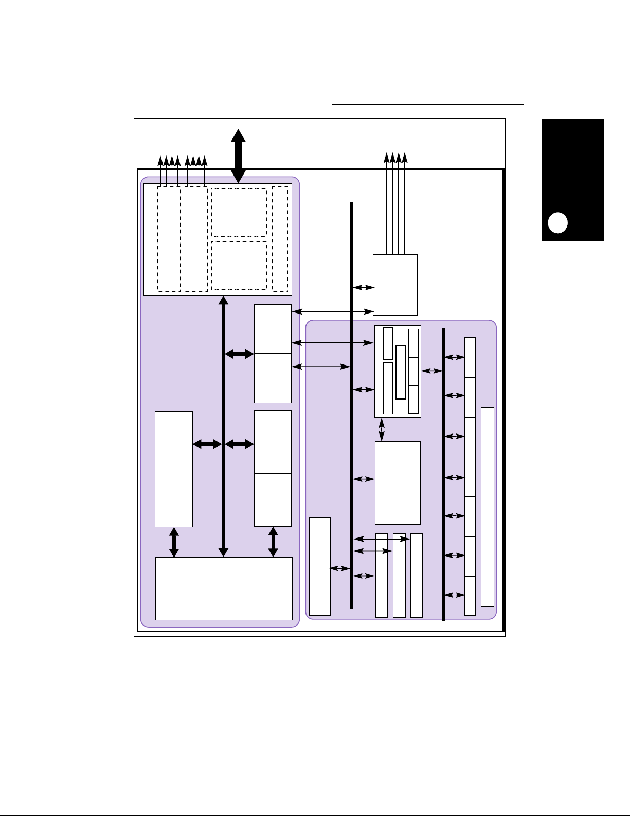
E_BUS
Introduction
PCMCIA INTERFACE
MEMORY CONTROLLER
SYSTEM INTERFACE UNIT
CORE
EXTENDED
CACHE
INSTRUCTION
MMU
INSTRUCTION
EXT_BIU
INT_BIU
SYSTEM FUNCTIONS
MASTER
INTERFACE
SLAVE
INTERFACE
COMMUNICATION
DATA MMU DATA CACHE
CPM LOCAL BUS
PROCESSOR
LCD
INTERFACE
CRC
MAC
REGISTER FILE
RISC MICROCONTROLLER
ALU
SEQUENCER ROM
RAM
DUAL-PORT
PERIPHERAL BUS
C
2
I
SCC3
INTRODUCTION
1
MOTOROLA
INTERRUPT
CORE
POWERPC
CONTROLLER
Figure 1-1. MPC823e Block Diagram
MPC823e REFERENCE MANUAL
TIMERS
PARALLEL I/O
SCC2 SMC1 SMC2
SERIAL INTERFACE AND TIME-SLOT ASSIGNER
USB SPI
BAUD RATE GENERATORS
1-7
Page 56

Introduction
1
INTRODUCTION
1.2.1 The Embedded PowerPC Core
The PowerPC core complies with standard PowerPC architecture. It has a fully static design
that consists of three functional blocks—the integer block, hardware multiplier/divider, and
load/store block. The core supports integer operations on a 32-bit internal data path and
32-bit arithmetic hardware. Its interface to the internal and external buses is 32 bits. The
core uses a two-instruction load/store queue, four-instruction prefetch queue, and a
six-instruction history buffer. It performs branch folding and branch prediction with
conditional prefetch, but without conditional execution. With single bus cycles, the core can
operate on 32-bit external operands and with critical-word-first in multiple bus cycles. The
PowerPC integer block supports 32 x 32-bit fixed-point general-purpose registers and can
execute one integer instruction per clock cycle.
The PowerPC core is integrated with the memory management units, an instruction cache,
and a data cache. The memory management units (MMUs) provide 32-entry,
fully-associative instruction and data TLBs, with multiple page sizes of 4K (1K protection),
16K, 512K, and 8M. They support 16 virtual address spaces and 16 protection groups.
Special registers are available to support software tablewalk and update.
The instruction cache is 16K, four-way, set-associative with physical addressing. It allows
single-cycle accesses on hit with no added latency for miss. It is four words per line and
supports burst line fill using an LRU replacement algorithm. The cache can be locked on a
line basis for application critical routines. The data cache is 8K, four-way, set-associative
with physical addressing. It allows single-cycle accesses on hit with one added clock latency
for miss. It has four words per line and supports burst line fill using an LRU replacement
algorithm. The cache can be locked on a line basis for application critical data and can be
programmed to support copyback or writethrough mode via the memory management unit.
The cache-inhibit mode can be programmed per MMU page. The PowerPC core, with its
instruction and data caches, can deliver approximately 99MIPS at 75MHz (using Dhrystone
2.1) or 172K Dhrystones, based on the assumption that it is issuing one instruction per cycle
with a cache hit rate of 94%.
1.2.2 The System Interface Unit
The system interface unit supports traditional 68K big-endian memory systems, traditional
x86 little-endian memory systems, and PowerPC little-endian memory systems. It also
provides power management functions, reset control, a PowerPC decrementer, PowerPC
timebase, and real-time clock. Although the PowerPC core is a 32-bit device internally, it can
be configured to operate with an 8-, 16-, or 32-bit data bus. Regardless of the system bus
size, dynamic bus sizing is supported, which allows 8-, 16-, and 32-bit peripherals and
memory to coexist on a 32-bit system bus.
The memory controller supports up to eight memory banks with glueless interfaces to
DRAM, SRAM, EPROM, Flash EPROM, SDRAM, EDO and other peripherals with two-clock
initial access to external SRAM and bursting support. It provides variable block sizes
between 32K and 256M. The memory controller has 0 to 20 wait states for each bank of
memory and can use address type matching to qualify each memory bank access. It
provides four byte-enable signals for varying width devices, one output-enable signal, and
one boot chip-select that is available at reset.
1-8 MPC823e REFERENCE MANUAL MOTOROLA
Page 57

Introduction
The DRAM interface supports 8-, 16-, and 32-bit ports and uses a programmable state
machine to support almost any memory interface. Memory banks can be defined in depths
of 256K, 512K, 1M, 2M, 4M, 8M, 16M, 32M, or 64M for all port sizes. In addition, the memory
depth can be defined as 64K and 128K for 8-bit memory or 128M and 256M for 32-bit
memory. The DRAM controller supports page mode access for successive transfers within
bursts. Although the MPC823e supports a glueless interface to DRAM, the capacitance of
the system bus may require that there be external buffers. The refresh unit provides CAS
before RAS
, a programmable refresh timer, refresh active during external reset, disable
refresh modes, and stacking for a maximum of seven refresh cycles.
1.2.3 The Communication Processor Module
The communication processor module (CPM) contains features that allow the MPC823e
microprocessor to excel in imaging, personal communication, and low-power applications.
These features are divided into three categories:
• DSP processing
• Communication processing
• Twelve serial DMA channels and two independent DMA channels
The MPC823e’s embedded DSP function allows the communication processor module to
execute imaging algorithms in parallel with the PowerPC core to achieve maximum
performance with very little power. The DSP can execute one 16x16 MAC on every clock
cycle. It has preprogrammed filtering functions like FIR, MOD, DEMOD, IIR, and
downloadable imaging functions for JPEG image compression and decompression. These
functions are also used by modem and speech recognition programs.
INTRODUCTION
1
The robust communication features of the MPC823e are provided by the communication
processor module. These features include a RISC microcontroller with multiply accumulate
(MAC) hardware, two serial communication controllers (SCCs), two serial management
controllers (SMCs), one dedicated serial channel for the universal serial bus (USB), one
2
inter-integrated circuit (I
C) port, one serial peripheral interface (SPI), 8K dual-port RAM, an
interrupt controller, a time-slot assigner, and four independent baud rate generators.
2
Twenty serial DMA channels support the SCCs, SMCs, USB channel, SPI, and I
C
controllers. The independent DMAs give you two channels for general-purpose DMA usage.
They offer high-speed transfers, 32-bit data movement, buffer chaining, and independent
request and acknowledge logic. The RISC microcontroller is the only block that can access
the IDMA registers directly. The CPU can only access them indirectly via a buffer descriptor.
MOTOROLA MPC823e REFERENCE MANUAL 1-9
Page 58

Introduction
1
INTRODUCTION
1.2.4 The Video/LCD Controller
The MPC823e has a dual-purpose video/LCD controller that shares common dual-port
memory. You can only run one of the controllers at a time.
1.2.4.1 THE VIDEO CONTROLLER. The video controller can be used to drive a digital
NTSC/PAL encoder or a wide variety of digital LCD panels. The frame buffer is stored in
system memory in the form of an orthogonal matrix—rows and columns. The 24-bit color
data is organized as pixel components whether it is sequential RGB or YC
rCb. Each pixel
component is represented by a byte. The video controller uses a dedicated DMA channel to
read the display data from the frame buffer and drive it to the video interface. It also
generates the required timing signals such as horizontal sync, vertical sync, field, and
blanking. Refer to Section 19 Video Controller for more information.
1.2.4.2 THE LCD CONTROLLER. The LCD controller provides extremely versatile LCD
support for 8-bit color, monochrome or 4/16-level grayscale, color TFT (12 bits, 4x3 RGB),
and passive color (xSTN) 4/8 bit data. The controller supports 4- or 8-bit single-scan, 2+2bit dual-scan, or 4+4-bit dual-scan. It is programmable for frame rate, number of pixels per
line, and number of lines per frame. The panel voltage is programmable through the duty
cycle for contrast adjustments implemented in the communication processor module
program. Display data is stored in your own memory space and is transferred into the
controller using the DMA channel. Refer to Section 18 LCD Controller for more
information.
1.3 THE PCMCIA-ATA CONTROLLER
The PCMCIA-ATA interface is a master controller that is compliant with Version 2.1 of the
PCMCIA standard. The interface supports one independent PCMCIA socket with the
required external transceivers or buffers. It provides eight memory or I/O windows that can
be allocated to the socket. If the PCMCIA port is not being used as a card interface, it can
provide eight general-purpose pins and two output-only pins with interrupt capability.
1-10 MPC823e REFERENCE MANUAL MOTOROLA
Page 59

Introduction
1.4 POWER MANAGEMENT
The MPC823e microprocessor supports a wide range of power management features,
including normal high, normal low, doze, sleep, deep-sleep, and power-down modes. In
normal high mode, the MPC823e microprocessor is fully powered with all internal units
operating at the full speed of the processor. Normal low mode is the same as normal high,
except it operates at a much lower frequency. There is a doze mode determined by a clock
divider that allows the operating system to reduce the operational frequency of the
processor.
Doze mode disables core functional units except the timebase, decrementer, PLL, memory
controller, real-time clock, LCD controller, and communication processor module. Sleep
mode is a lower power mode that disables everything except the real-time clock, timebase,
decrementer, and periodic interrupt timer, thus leaving the PLL active for quick wake-up.
The deep-sleep mode then disables the PLL for lower power, but slower wake-up.
Power-down mode disables all logic in the processor, except the minimum logic required to
restart the device. It saves the most power, but requires the longest wake-up time.
1.5 SYSTEM DEBUG SUPPORT
The MPC823e microprocessor contains an advanced debug interface that provides superior
debug capabilities without any loss of speed. It supports six watchpoint pins that can be
combined with eight internal comparators, four of which operate on the effective address of
the address bus. The other four comparators are split—two comparators operate on the
effective address on the data bus and two comparators operate on the data on the data bus.
The MPC823e microprocessor can compare using the =, ≠, <, and > conditions to generate
watchpoints. Each watchpoint can then generate a breakpoint that can be programmed to
trigger in a programmable number of events.
INTRODUCTION
1
1.6 APPLICATIONS
The MPC823e microprocessor is specifically designed to be a general-purpose, low-cost
entry point to the Motorola embedded PowerPC Family for systems in which advanced
GUIs, communications, and high-level real-time operating systems are used. The device
excels in applications that require the performance of single-issue PowerPC core with a
moderate amount of data and instruction cache. It provides all the basic features of glueless
memory connections along with functional serial connectivity, a graphical LCD, and a video
display controller. The MPC823e excels in low-power and portable applications because of
its extensive power-down modes and low normal operation current.
MOTOROLA MPC823e REFERENCE MANUAL 1-11
Page 60

Introduction
1
INTRODUCTION
1.7 DIFFERENCES BETWEEN MPC823 (REV 1) AND MPC823e
The following modifications were made to the MPC823 Revision 1 to create the MPC823e:
• Core operation was increased to 99MIPS @ 75MHz or 172K Dhyrstones
• The instruction cache was increased to 16K
• There are twenty serial DMA channels for reception and transmission
• The data cache was increased to 8K
• The instruction and data memory management units each consist of 32 TLB entries
• A time-division multiplex channel (TDMB) was added to the serial interface
1.8 MPC823e GLUELESS SYSTEM DESIGN
The MPC823e was primarily designed to make it easy for you to interface a microprocessor
with other system components. Figure 1-2 illustrates a system configuration that contains
one flash EPROM and yet supports DRAM SIMM and one SRAM. Although the MPC823e
supports a glueless interface to DRAM, the capacitance of the system bus may require that
there be external buffers. From a logic standpoint, however, a glueless system is
maintained.
1-12
MPC823e REFERENCE MANUAL
MOTOROLA
Page 61
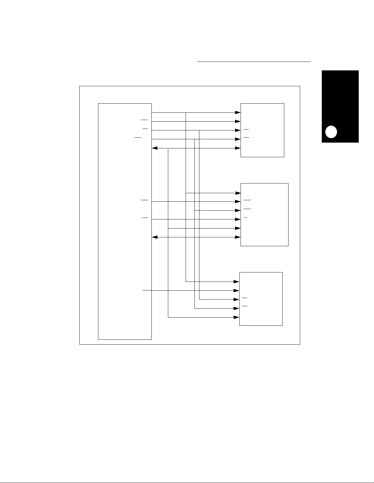
8-BIT BOOT
EPROM/FLASH
Introduction
ADDRESS
CS0
GPL1/
MPC823e
WE[
DATA
OE
0:3]
WE0
CS1
RD/
WR
PARITY[0:3] PARITY[0:3]
CS2
ADDRESS
CE
CE
OE
OE
WE
DATA
DRAM
ADDRESS
RAS
CAS
[0:3]
W
W
DATA
SRAM
ADDRESS
CE
CE
OE
OE
WE
DATA
INTRODUCTION
1
Figure 1-2. MPC823e System Configuration
MOTOROLA MPC823e REFERENCE MANUAL 1-13
Page 62
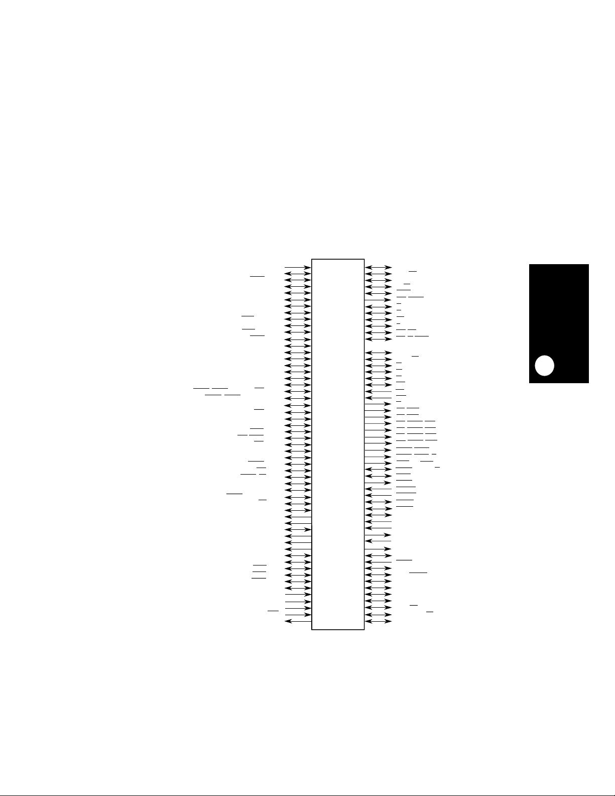
SECTION 2 EXTERNAL SIGNALS
This section briefly describes each of the MPC823e input and output signals.
VDDSYN/VSSSYN/VSSSYN1/VDDH/VDDL/VSS/KAPWR
TIN1/L1RCLKA/BRGO1/CLK1/PA[7]
TIN3/L1RCLKB/TOUT1/CLK2/PA[6]
TIN2/L1TCLKA/BRGO2/CLK3/PA[5]
TIN4/L1TCLKB/TOUT2/CLK4/PA[4]
SMSYN1/SDACK1/L1TSYNCB/CTS3/PB[23]
SMSYN2/SDACK2/L1RSYNCB/PB[22]
USBRXD/PA[15]
USBOE/PA[14]
RXD2/PA[13]
TXD2/PA[12]
SMRXD2/L1TXDA/PA[9]
SMTXD2/L1RXDA/PA[8]
LCD_A/SPISEL/PB[31]
SPICLK/TXD3/PB[30]
SPIMOSI/RXD3/PB[29]
BRGO3/SPIMISO/PB[28]
BRGO1/I2CSDA/PB[27]
BRGO2/I2CSCL/PB[26]
SMTXD1/TXD3/PB[25]
SMRXD1/L1RXDB/RXD3/PB[24]
LCD_B/L1ST1/PB[19]
L1ST2/RTS2/PB[18]
LCD_C/L1ST3/PB[17]
L1ST4/L1RQA/PB[16]
L1ST5/L1TXDB/DREQ1/PC[15]
L1ST6/RTS2/DREQ2/PC[14]
L1ST7/RTS3/PC[13]
L1ST8/L1RQA/PC[12]
USBRXP/PC[11]
USBRXN/TGATE1/PC[10]
CTS2/PC[9]
TGATE1/CD2/PC[8]
USBTXP/PC[7]
USBTXN/PC[6]
SDACK1/L1TSYNCA/PC[5]
L1RSYNCA/CD3/PC[4]
LD8/VD7/PD[15]
LD7/VD6/PD[14]
LD6/VD5/PD[13]
LD5/VD4/PD[12]
LD4/VD3/PD[11]
LD3/VD2/PD[10]
LD2/VD1/PD[9]
LD1/VD0/PD[8]
LD0/FIELD/PD[7]
LCD_AC/LOE/BLANK/PD[6]
FRAME/VSYNC/PD[5]
LOAD/HSYNC/PD[4]
SHIFT/CLK/CLK/PD[3]
TMS
TDI/DSDI
TCK/DSCK
TRST
TDO/DSDO
1
1
1
1
1
1
1
1
1
1
1
1
1
1
1
1
1
1
1
1
1
1
1
1
1
1
1
1
1
1
1
1
1
1
1
1
1
1
1
1
1
1
1
1
1
1
1
1
1
1
1
1
1
1
MPC823e
26
1
1
1
1
1
1
1
1
1
1
1
32
4
1
1
1
1
2
1
6
1
1
1
1
1
1
1
1
2
1
1
1
1
1
1
1
1
1
1
1
1
1
1
1
2
1
1
1
1
1
2
1
1
A[6:31]
TSIZ0/REG
TSIZ1
RD/WR
BURST
BDIP/GPL_B5
TS
TA
TEA
BI
IRQ2/RSV
IRQ4/KR/RETRY/SPKROUT
D[0:31]
DP[0:3]/IRQ[3:6]
BR
BG
BB
IRQ6/FRZ
IRQ[0:1]
IRQ7
CS[0:5]
CS6/CE1_B
CS7/CE2_B
WE0/BS_AB0/IORD
WE1/BS_AB1/IOWR
WE2/BS_AB2/PCOE
WE3/BS_AB3/PCWE
GPL_A0/GPL_B0
GPL_A1/GPL_B1/OE
GPL_A[2:3]/GPL_B[2:3]
GPL_A4/UPWAITA/AS
GPL_B4/UPWAITB
GPL_A5
PORESET
RSTCONF
HRESET
SRESET
XTAL
EXTAL
XFC
CLKOUT
EXTCLK
TEXP
ALE_B/DSCK/AT1
WAIT_B
IP_B[0:1]/IWP[0:1]/VFLS[0:1]
IP_B2/IOIS16_B/AT2
IP_B3/IWP2/VF2
IP_B4/LWP0/VF0
IP_B5/LWP1/VF1
IP_B6/DSDI/AT0
IP_B7/PTR/AT3
MODCK1/OP2/STS
MODCK2/OP3/DSDO
EXTERNAL SIGNALS
2
MOTOROLA
Figure 2-1. MPC823e Signal Pinout
MPC823e REFERENCE MANUAL
2-1
Page 63
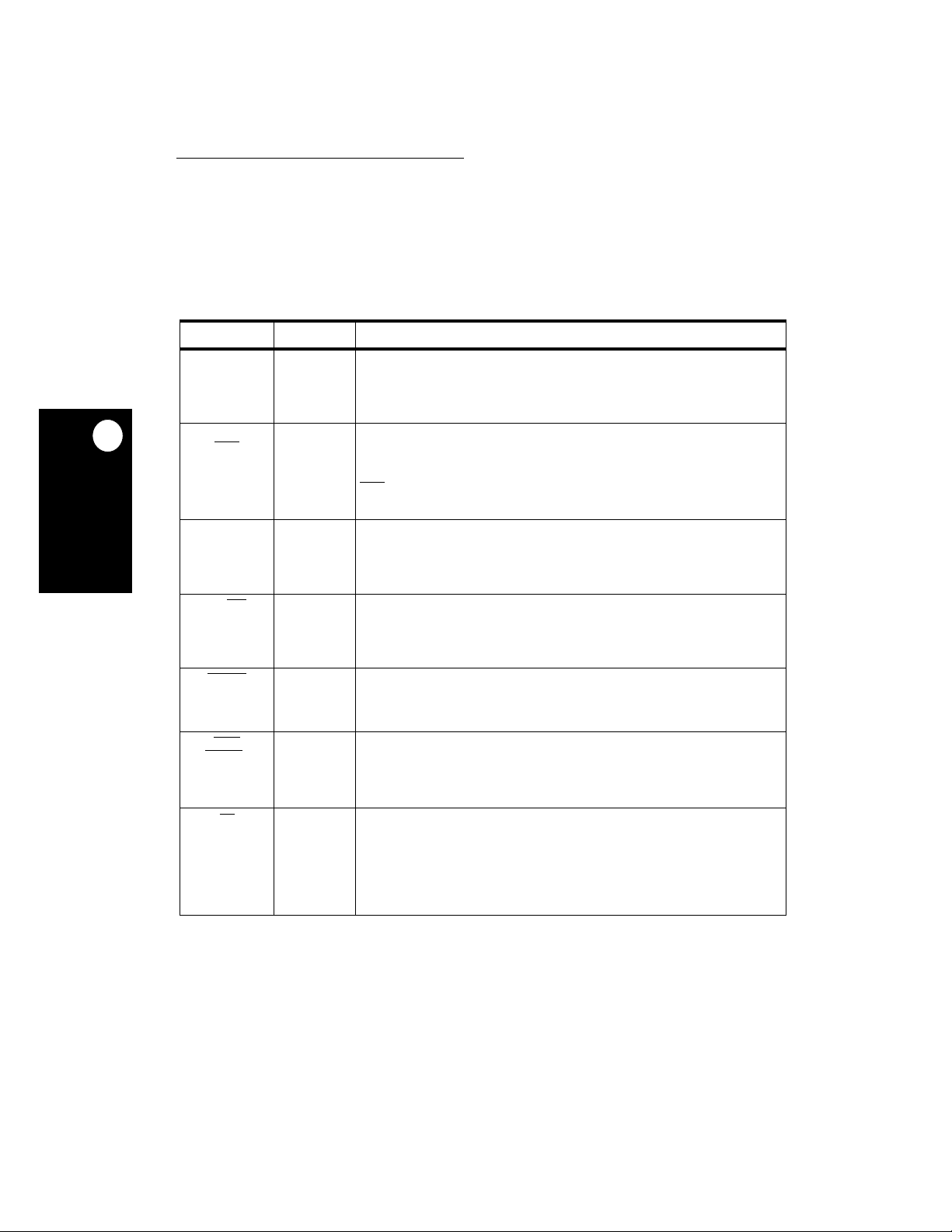
External Signals
2.1 THE SYSTEM BUS SIGNALS
The MPC823e system bus signals consist of all the lines that interface with the external bus.
Many of these lines perform different functions, depending on how you assign them. The
following input and output signals are identified by their mnemonic name and each signal’s
pin number can be found in Figure 2-1.
Table 2-1. Signal Descriptions
SIGNAL PIN NUMBER DESCRIPTION
2
EXTERNAL SIGNALS
A[6:31] See Table 2-2
TSIZ0
REG
TSIZ1 E15
C13
RD/WR
BURST
BDIP
GPL_B5
TS
for pin
breakout.
F15
B10
A13
D10
Address Bus— This bidirectional three-state signal provides the address for the
current bus cycle. A6 is the most-significant signal for this bus. The signal is output
when an internal master on the MPC823e initiates a transaction on the external bus.
The signal is input when an external master initiates a transaction on the bus and it
is sampled internally to allow the memory controller/PCMCIA interface to control the
accessed slave device.
Transfer Size 0 —When accessing a slave in the external bus, this three-state signal
is used (together with TSIZ1) by the bus master to indicate the number of operand
bytes waiting to be transferred in the current bus cycle. This signal is input when an
external master initiates a transaction on the bus and it is sampled internally to allow
the memory controller/PCMCIA interface to control the accessed slave device.
REG
—When the access is initiated by an internal master to a slave under control of
the PCMCIA interface, this signal is output to indicate which space in the PCMCIA
card is currently accessed.
Transfer Size 1— This three-state signal is used (with TSIZ0) by the bus master to
indicate the number of operand bytes waiting to be transferred in the current bus
cycle. This signal is driven by the MPC823e when it is the owner of the bus. It is input
when an external master initiates a transaction on the bus and it is sampled internally
to allow the memory controller/PCMCIA interface to control the accessed slave
device.
Read Write —This three-state signal is driven by the bus master to indicate the
direction of the bus’s data transfer. A logic one indicates a read from a slave device
and a logic zero indicates a write to a slave device. This signal is driven by the
MPC823e when it is the owner of the bus. It is input when an external master initiates
a transaction on the bus and is sampled internally to allow the memory controller/
PCMCIA interface to control the accessed slave device.
Burst Transaction —This three-state signal is driven by the bus master to indicate
that the current initiated transfer is a burst one. This signal is driven by the MPC823e
when it is the owner of the bus. It is input when an external master initiates a
transaction on the bus; this signal and is sampled internally to allow the memory
controller/PCMCIA interface to control the accessed slave device.
Burst Data in Progress —When accessing a slave device in the external bus, the
master on the bus asserts this signal to indicate that the data beat in front of the
current one is the one requested by the master. This signal is negated prior to the
expected last data beat of the burst transfer.
General-Purpose Line B5 —This signal is used by the memory controller when the
user programmable machine B (UPMB) takes control of the slave access.
Transfer Start— This three-state signal is asserted by the bus master to indicate the
start of a bus cycle that transfers data to or from a slave device. This signal is driven
by the master only when it has gained ownership of the bus. Every master should
negate this signal before the bus relinquishes. A pull-up resistor should be connected
to this signal to prevent a slave device from detecting a spurious bus accessing it
when no master is taking ownership of the bus.
This signal is sampled by the MPC823e when it is not the owner of the external bus
to allow the memory controller/PCMCIA interface to control the accessed slave
device. It indicates that an external synchronous master initiated a transaction.
2-2
MPC823e REFERENCE MANUAL
MOTOROLA
Page 64
External Signals
Table 2-1. Signal Descriptions (Continued)
SIGNAL PIN NUMBER DESCRIPTION
TA
TEA
BI B12
RSV
IRQ2
IRQ4
KR
RETRY
SPKROUT
D[0:31] See Table 2-2
DP0
3
IRQ
DP1
IRQ4
A12
C11
D9
B7
for pin
breakout.
C3
D4
Transfer Acknowledge —This bidirectional three-state signal indicates that the
slave device addressed in the current transaction has accepted the data transferred
by the master (write) or has driven the data bus with valid data (read). The signal
behaves as an output when the PCMCIA memory controller takes control of the
transaction. The only exception occurs when the memory controller is controlling the
slave access by means of the GPCM and the corresponding option register is
instructed to wait for an external assertion of the transfer acknowledge line. Every
slave device should negate the ta signal after the end of the transaction and
immediately three-state it to avoid contentions on the line if a new transfer is initiated
addressing other slave devices. A pull-up resistor should be connected to this signal
to keep a master device from detecting the assertion of this signal when no slave is
addressed in a transfer or when the address detection for the addressed slave is
slow.
Transfer Error Acknowledge —This open-drain signal indicates that a bus error
occurred in the current transaction. It is driven asserted by the MPC823e when the
bus monitor does not detect a bus cycle termination within a reasonable amount of
time. The assertion of TEA
ignoring the state of TA
Burst Inhibit —This bidirectional three-state signal indicates that the slave device
addressed in the current burst transaction is unable to support burst transfers. The
signal behaves as an output when the PCMCIA memory controller takes control of
the transaction. When the MPC823e drives out the signal for a specific transaction,
it asserts or negates BI
the appropriate control registers. It negates the signal after the end of the transaction
and immediately three-states it to avoid contentions if a new transfer is initiated
addressing other slave devices.
Reservation —This three-state signal is output by the MPC823e in conjunction with
the address bus to indicate that the internal core initiated a transfer as a result of a
stwcx or lwarx instruction.
Interrupt Request 2 —This input is one of the eight external signals that can request
(by means of the internal interrupt controller) a service routine from the core.
Interrupt Request 4 —This input signal is one of the eight external signals that can
request (by means of the internal interrupt controller) a service routine from the core.
It should be noted that the interrupt request signal that is sent to the interrupt
controller is the logical AND of this signal (if defined to function as IRQ4
DP1/IRQ4
Kill Reservation —This input is used as a part of the storage reservation protocol
when the MPC823e initiated a transaction as the result of a stwcx instruction.
Retry— This input is used by the slave device to indicate that it is unable to accept
the transaction. The MPC823e has to relinquish the ownership of the bus and initiate
the transaction again after winning again in the bus arbitration.
Speaker Out —This output signal is used to provide a digital audio waveform to be
driven to the system’s speaker.
Data Bus —This bidirectional three-state signal provides the general-purpose data
path between the MPC823e and all other devices. Although the data path is a
maximum of 32 bits wide, it can be dynamically sized to support 8-, 16-, or 32-bit
transfers. D0 is the most-significant bit of the data bus.
Data Parity 0 —This bidirectional three-state signal provides parity generation and
checking for the data bus lane D[0:7] by transferring to a slave device initiated by the
MPC823e. The parity function can be defined independently for each one of the
addressed memory banks (if controlled by the memory controller) and for the rest of
the slaves on the external bus.
Interrupt Request 3 —This input signal is one of the eight external signals that can
request (by means of the internal interrupt controller) a service routine from the core.
Data Parity 1 —This bidirectional three-state signal provides parity generation and
checking for the data bus lane D[8:15] by transferring to a slave device initiated by
the MPC823e. The parity function can be defined independently for each one of the
addressed memory banks (if controlled by the memory controller) and for the rest of
the slaves on the external bus.
Interrupt Request 4 —This input is one of the eight external lines that can request
(by means of the internal interrupt controller) a service routine from the core. It should
be noted that the interrupt request signal that is sent to the interrupt controller is the
logical AND of this signal (if defined to function as IRQ4
IRQ4 if defined to function as IRQ4.
(if defined to function as IRQ4).
causes the termination of the current bus cycle, thus
.
during the transaction according to the value you specify in
) and the
) and the KR/SPKROUT/
EXTERNAL SIGNALS
2
MOTOROLA
MPC823e REFERENCE MANUAL
2-3
Page 65
External Signals
2
EXTERNAL SIGNALS
Table 2-1. Signal Descriptions (Continued)
SIGNAL PIN NUMBER DESCRIPTION
DP2
IRQ5
DP3
IRQ6
BR B11
BG
BB
IRQ6
FRZ
IRQ0 N1
IRQ1
IRQ7
[0:5] See Table 2-2
CS
CS6
CE1_B
D3
C2
C10
A11
A10
N2
N3
for pin
breakout.
C14
Data Parity 2 —This bidirectional three-state signal provides parity generation and
checking for the data bus lane D[16:23] by transferring to a slave device initiated by
the MPC823e. The parity function can be defined independently for each one of the
addressed memory banks (if controlled by the memory controller) and for the rest of
the slaves on the external bus.
Interrupt Request 5 —This input signal is one of the eight external signals that can
request (by means of the internal interrupt controller) a service routine from the core.
Data Parity 3 —This bidirectional three-state signal provides parity generation and
checking for the data bus lane D[24:31] by transferring to a slave device initiated by
the MPC823e. The parity function can be defined independently for each one of the
addressed memory banks (if controlled by the memory controller) and for the rest of
the slaves on the external bus.
Interrupt Request 6 —This input signal is one of the eight external signals that can
request (by means of the internal interrupt controller) a service routine from the core.
It should be noted that the interrupt request signal that is sent to the interrupt
controller is the logical AND of this signal (if defined to function as IRQ6
FRZ/IRQ6
Bus Request —This bidirectional signal is asserted low when a possible master is
requesting ownership of the bus. When the MPC823e is configured to operate with
the internal arbiter, this signal is configured as an input. However, when the
MPC823e is configured to operate with an external arbiter, this signal is configured
as an output and asserted every time a new transaction is intended to be initiated
and no parking on the bus is granted.
Bus Grant —This bidirectional signal is asserted low when the arbiter of the external
bus grants the specific master ownership of the bus. When the MPC823e is
configured to operate with the internal arbiter, this signal is configured as an output
and asserted every time the external master asserts the BR
request is higher than any of the internal sources requiring the initiation of a bus
transfer. However, when the MPC823e is configured to operate with an external
arbiter, this signal is configured as an input.
Bus Busy —This bidirectional signal is asserted low by a master to show that it owns
the bus. The MPC823e asserts this signal after the bus arbiter grants it bus
ownership and the BB
Interrupt Request 6 —This input signal is one of the eight external signals that can
request (by means of the internal interrupt controller) a service routine from the core.
It should be noted that the interrupt request signal that is sent to the interrupt
controller is the logical AND of this signal (if defined to function as IRQ6
DP3/IRQ6
Freeze —This output signal is asserted to indicate that the internal core is in debug
mode.
Interrupt Request 0 —This input signal is one of the eight external signals that can
request (by means of the internal interrupt controller) a service routine from the core.
It causes a non-maskable interrupt to the core.
Interrupt Request 1 —This input signal is one of the eight external signals that can
request (by means of the internal interrupt controller) a service routine from the core.
Interrupt Request 7 —This input signal is one of the eight external signals that can
request (by means of the internal interrupt controller) a service routine from the core.
Chip Select —These output signals enable peripheral or memory devices at
programmed addresses if they are appropriately defined in the memory controller.
CS0
Chip Select 6 —This output signal enables a peripheral or memory device at a
programmed address if defined appropriately in the BR6 and OR6 of the memory
controller.
Card Enable 1 Slot B —This output signal enables even byte transfers when
accesses to the PCMCIA Slot B are handled by the PCMCIA interface.
if defined to function as IRQ6.
signal is negated.
(if defined to function as IRQ6.)
can be configured to be the global chip-select for the boot device.
) and the
signal and its priority
) and the
2-4
MPC823e REFERENCE MANUAL
MOTOROLA
Page 66
Table 2-1. Signal Descriptions (Continued)
SIGNAL PIN NUMBER DESCRIPTION
CS7
CE2_B
WE0
BS_AB0
IORD
WE1
BS_AB1
IOWR
WE2
BS_AB2
PCOE
WE3
BS_AB3
PCWE
GPL_A0
GPL_B0
GPL_A1
GPL_B1
OE
B15
D16
E16
D15
F13
E13
C16
Chip Select 7 —This output signal enables a peripheral or memory device at a
programmed address if defined appropriately in the BR7 and OR7 registers of the
memory controller.
Card Enable 2 Slot B —This output signal enables odd byte transfers when
accesses to the PCMCIA Slot B are handled by the PCMCIA interface.
Write Enable 0 —This output signal is asserted when a write access to an external
slave controlled by the GPCM in the memory controller is initiated by the MPC823e.
is asserted if the data lane D[0:7] contains valid data to be stored by the slave
WE0
device.
Byte Select 0 on UPMA or UPMB —This output signal is asserted as required by
the UPMA or UPMB in the memory controller whenever you program it. In a read or
write transfer, the signal is only asserted if the data lane D[0:7] contains valid data.
I/O Device Read —This output signal is asserted when the MPC823e initiates a read
access to a region controlled by the PCMCIA interface. The signal is only asserted if
the access is to a PC Card I/O space.
Write Enable 1 —This output signal is asserted when the MPC823e initiates a write
access to an external slave controlled by the GPCM in the memory controller. WE1
is asserted if the data lane D[8:15] contains valid data to be stored by the slave
device.
Byte Select 1 on UPMA or UPMB —This output signal is asserted as required by
the UPMA or UPMB in the memory controller whenever you program it. In a read or
write transfer, the signal is only asserted if the data lane D[8:15] contains valid data.
I/O Device Write —This output signal is asserted when the MPC823e initiates a write
access to a region controlled by the PCMCIA interface. The signal is only asserted if
the access is to a PC Card I/O space.
Write Enable 2 —This output signal is asserted when the MPC823e initiates a write
access to an external slave controlled by the GPCM in the memory controller. WE2
is asserted if the data lane D[16:23] contains valid data to be stored by the slave
device.
Byte Select 2 on UPMA or UPMB —This output signal is asserted as required by
the UPMA or UPMB in the memory controller whenever you program it. In a read or
write transfer, the signal is only asserted if the data lane D[16:23] contains valid data.
PCMCIA Output Enable —This output signal is asserted when the MPC823e
initiates a read access to a memory region under the control of the PCMCIA
interface.
Write Enable 3 —This output signal is asserted when the MPC823e initiates a write
access to an external slave controlled by the GPCM in the memory controller. WE3
is asserted if the data lane D[24:31] contains valid data to be stored by the slave
device.
Byte Select 3 on UPMA or UPMB —This output signal is asserted as required by
the UPMA or UPMB in the memory controller whenever you program it. In a read or
write transfer, the signal is only asserted if the data lane D[24:31] contains valid data.
PCMCIA Write Enable —This output signal is asserted when the MPC823e initiates
a write access to a memory region controlled by the PCMCIA interface.
General-Purpose Line 0 on UPMA —This output signal reflects the value specified
in the UPMA in the memory controller when an external transfer to a slave is
controlled by the user programmable machine A (UPMA).
General-Purpose Line 0 on UPMB —This output signal reflects the value specified
in the UPMB in the memory controller when an external transfer to a slave is
controlled by the user programmable machine B (UPMB).
General-Purpose Line 1 on UPMA —This output signal reflects the value specified
in the UPMA in the memory controller when an external transfer to a slave is
controlled by the user programmable machine A (UPMA).
General-Purpose Line 1 on UPMB —This output signal reflects the value specified
in the UPMB in the memory controller when an external transfer to a slave is
controlled by the user programmable machine B (UPMB).
Output Enable —This output signal is asserted when the MPC823e initiates a read
access to an external slave controlled by the GPCM in the memory controller.
External Signals
EXTERNAL SIGNALS
2
MOTOROLA
MPC823e REFERENCE MANUAL
2-5
Page 67
External Signals
2
EXTERNAL SIGNALS
UPWAITA
UPWAITB
PORESET
RSTCONF
Table 2-1. Signal Descriptions (Continued)
SIGNAL PIN NUMBER DESCRIPTION
2
GPL_A
GPL_B2
CS2
3
GPL_A
GPL_B3
CS3
GPL_A4
AS
4
GPL_B
GPL_A5
HRESET
SRESET
XTAL A4
EXTAL A5
XFC B2
CLKOUT D1
EXTCLK A6
C15
D14
D11
B13
C12
B3
C5
B5
B4
General-Purpose Line 2 on UPMA —This output signal reflects the value specified
in the UPMA in the memory controller when an external transfer to a slave is
controlled by the user programmable machine A (UPMA).
General-Purpose Line 2 on UPMB —This output signal reflects the value specified
in the UPMB in the memory controller when an external transfer to a slave is
controlled by the user programmable machine B (UPMB).
Chip Select 2 —This output signal enables a peripheral or memory device at a
programmed address if defined appropriately in the BR2 and OR2 registers of the
memory controller.
General-Purpose Line 3 on UPMA —This output signal reflects the value specified
in the UPMA in the memory controller when an external transfer to a slave is
controlled by the user programmable machine A (UPMA).
General-Purpose Line 3 on UPMB —This output signal reflects the value specified
in the UPMB in the memory controller when an external transfer to a slave is
controlled by the user programmable machine B (UPMB).
Chip Select 3 —This output signal enables a peripheral or memory device at a
programmed address if defined appropriately in the BR3 and OR3 registers of the
memory controller.
General-Purpose Line 4 on UPMA —This output signal reflects the value specified
in the UPMA in the memory controller when an external transfer to a slave is
controlled by the user programmable machine A (UPMA).
User Programmable Machine Wait A —This input signal is sampled when you need
it and when an access to an external slave is controlled by the UPMA in the memory
controller.
Address Strobe —This input pin is driven by an external asynchronous master to
indicate a valid address on the A[6:31] lines. The memory controller in the MPC823e
will synchronize this signal and control the memory device addressed if it is
recognized to be under its control.
General-Purpose Line 4 on UPMB —This output signal reflects the value specified
in the UPMB in the memory controller when an external transfer to a slave is
controlled by the user programmable machine B (UPMB).
User Programmable Machine Wait B —This input signal is sampled when you need
it and when an access to an external slave is controlled by the UPMB in the memory
controller.
General-Purpose Line 5 on UPMA —This output signal reflects the value specified
in the UPMA in the memory controller when an external transfer to a slave is
controlled by the user programmable machine A (UPMA). This signal can also be
controlled by the UPMB.
Power-On Reset —When asserted, this input signal causes the MPC823e to enter
the power-on reset state.
Reset Configuration —This input signal is sampled by the MPC823e during the
assertion of the HRESET
in the form of the hard reset configuration word driven on the data bus. When this
signal is negated, the default configuration mode is adopted by the MPC823e. Notice
that the initial base address of internal registers is determined in this sequence.
Hard Reset —This open drain line, when asserted, causes the MPC823e to enter the
hard reset state.
Soft Reset —This open drain line, when asserted, causes the MPC823e to enter the
soft reset state.
External Crystal —This output signal is one of the connections to an external crystal
for the internal oscillator circuitry.
External Crystal —This signal is one of the connections to an external crystal for the
internal oscillator circuitry.
External Filter Capacitance —This input signal is the connection pin to an external
capacitor filter for the PLL circuitry.
CLKOUT —This output signal is the clock system frequency.
External Clock —This input signal is the external input clock from an external
source.
signal. If it is asserted, the configuration mode is sampled
2-6
MPC823e REFERENCE MANUAL
MOTOROLA
Page 68
Table 2-1. Signal Descriptions (Continued)
SIGNAL PIN NUMBER DESCRIPTION
TEXP D5
WAIT_B
ALE_B
DSCK
AT1
IP_B0
IWP0
VFLS0
IP_B1
IWP1
VFLS1
IP_B2
IOIS16_B
AT2
IP_B3
IWP2
VF2
IP_B4
LWP0
VF0
IP_B5
LWP1
VF1
C4
B8
A8
C8
D7
A9
B9 Input Port B 4—This input signal is monitored by the MPC823e and its value and
C9 Input Port B 5—This input signal is monitored by the MPC823e and its value and
Timer Expired —This output signal reflects the status of the TEXPS bit of the
PLPRCR register in the clock interface.
Wait Slot B —This input signal, if asserted low, causes the completion of a
transaction to be delayed on the PCMCIA-controlled Slot B.
Address Latch Enable B —This output signal is asserted when the MPC823e
initiates an access to a region under the control of the PCMCIA socket B interface.
Development Serial Clock —This input signal is the clock for the debug port
interface.
Address Type 1 —This bidirectional three-state signal is driven by the MPC823e
when it initiates a transaction on the external bus. When the transaction is initiated
by the internal core, it indicates if the transfer is for problem or privilege state.
Input Port B 0 —This input signal is sensed by the MPC823e and its value and
changes are reported in the PIPR and PSCR registers of the PCMCIA interface.
Instruction Watchpoint 0 —This output signal reports the detection of an instruction
watchpoint in the program flow executed by the internal core.
Visible History Buffer Flushes Status —This output signal is output by the
MPC823e when you need program instructions flow tracking. It reports the number
of instructions flushed from the history buffer in the internal core.
Input Port B 1 —This input signal is sensed by the MPC823e and its value and
changes are reported in the PIPR and PSCR registers of the PCMCIA interface.
Instruction Watchpoint 1 —This output signal reports the detection of an instruction
watchpoint in the program flow executed by the internal core.
Visible History Buffer Flushes Status —This output signal is output by the
MPC823e when you need program instructions flow tracking. It reports the number
of instructions flushed from the history buffer in the internal core.
Input Port B 2 —This input signal is sensed by the MPC823e and its value and
changes are reported in the PIPR and PSCR registers of the PCMCIA interface.
I/O Device B is 16 Bits Port Size —This input signal is monitored by the MPC823e
when a PCMCIA interface transaction is initiated to an I/O region in socket B within
the PCMCIA space.
Address Type 2 —This bidirectional three-state signal is driven by the MPC823e
when it initiates a transaction on the external bus. When the transaction is initiated
by the internal core, it indicates if the transfer is instruction or data.
Input Port B 3 —This input signal is monitored by the MPC823e and its value and
changes are reported in the PIPR and PSCR registers of the PCMCIA interface.
Instruction Watchpoint 2 —This output signal reports the detection of an instruction
watchpoint in the program flow executed by the internal core.
Visible Instruction Queue Flush Status —This output signal, together with VF0 and
VF1, is output by the MPC823e when you need program instruction flow tracking.
VFx reports the number of instructions flushed from the instruction queue in the
internal core.
changes are reported in the PIPR and PSCR registers of the PCMCIA interface.
Load/Store Watchpoint 0—This output signal reports the detection of a data
watchpoint in the program flow executed by the internal core.
Visible Instruction Queue Flushes Status—This output signal, together with VF1
and VF2, is output by the MPC823e when you need program instructions flow
tracking. VF reports the number of instructions flushed from the instruction queue in
the internal core.
changes are reported in the PIPR and PSCR registers of the PCMCIA interface.
Load/Store Watchpoint 1—This output signal reports the detection of a data
watchpoint in the program flow executed by the internal core.
Visible Instruction Queue Flushes Status—This output signal, together with VF0
and VF2, is output by the MPC823e when you need program instructions flow
tracking. VF reports the number of instructions flushed from the instruction queue in
the internal core.
External Signals
EXTERNAL SIGNALS
2
MOTOROLA
MPC823e REFERENCE MANUAL
2-7
Page 69
External Signals
2
EXTERNAL SIGNALS
Table 2-1. Signal Descriptions (Continued)
SIGNAL PIN NUMBER DESCRIPTION
IP_B6
DSDI
AT0
IP_B7
PTR
AT3
MODCK1
OP2
STS
MODCK2
OP3
DSDO
PA[15]
USBRXD
PA[14]
USBOE
PA[13]
RXD2
PA[12]
TXD2
PA[9]
L1TXDA
SMRXD2
PA[8]
L1RXDA
SMTXD2
PA[7]
CLK1
TIN1
L1RCLKA
BRGO1
PA[6]
CLK2
TOUT1
TIN3
L1RCLKB
C7 Input Port B 6—This input signal is sensed by the MPC823e and its value and
D8 Input Port B 7—This input signal is monitored by the MPC823e and its value and
D6 Mode Clock 1—This input signal is sampled at PORESET negation to configure the
B6 Mode Clock 2—This input signal is sampled at PORESET
P16 General-Purpose I/O Port A Bit 15—Bit 15 of the general-purpose I/O port A.
R15 General-Purpose I/O Port A Bit 14—Bit 14 of the general-purpose I/O port A.
R14 General-Purpose I/O Port A Bit 13—Bit 13 of the general-purpose I/O port A.
R13 General-Purpose I/O Port A Bit 12—Bit 12 of the general-purpose I/O port A.
N10 General-Purpose I/O Port A Bit 11—Bit 9 of the general-purpose I/O port A.
T9 General-Purpose I/O Port A Bit 8—Bit 8 of the general-purpose I/O port A.
T8 General-Purpose I/O Port A Bit 7—Bit 7 of the general-purpose I/O port A.
P8 General-Purpose I/O Port A Bit 6—Bit 6 of the general-purpose I/O port A.
changes are reported in the PIPR and PSCR registers of the PCMCIA interface.
Development Serial Data Input—This input signal is the data in for the debug port
interface.
Address Type 0—This bidirectional three-state signal is driven by the MPC823e
when it initiates a transaction on the external bus. If high (1), the transaction is the
CPM. If low (0), the transaction initiator is the core.
changes are reported in the PIPR and PSCR registers of the PCMCIA interface.
Program Trace—This output signal is asserted by the MPC823e to indicate that an
instruction fetch is taking place in order to allow program flow tracking.
Address Type 3—This bidirectional three-state signal is driven by the MPC823e
when it initiates a transaction on the external bus. When the transaction is initiated
by the internal core, it indicates if the transfer is reserved for data transfers or a
program trace indication for instructions fetch.
PLL/clock mode of operation.
Output Port 2—This output signal is generated by the MPC823e as a result of a
write to the PGCRB register in the PCMCIA interface.
Special Transfer Start—This output signal is driven by the MPC823e to indicate the
beginning of a transaction on the external bus or an internal transaction in show cycle
mode.
PLL/clock mode of operation.
Output Port 3—This output signal is generated by the MPC823e as a result of a
write to the PGCRB register in the PCMCIA interface.
Development Serial Data Output—This output signal is the data out of the debug
port interface.
USBRXD—The receive data input signal for the USB.
USBOE—The output enable signal for the USB transmitter.
RXD2—The receive data input signal for serial communication controller 2.
TXD2—The transmit data output signal for serial communication controller 2. TXD2
has open-drain capability.
L1TXDA—The transmit data output signal for the serial interface time-division
multiplex port A. This signal has open-drain capability.
SMRXD2—The serial management controller 2 receive data pin.
L1RXDA—The receive data input signal for the serial interface time-division
multiplex port A.
SMTXD2—The serial management controller 2 transmit data pin.
CLK1—This input signal is one of the four clock pins that can be used to clock the
serial communication controllers, serial management controllers, and USB.
TIN1—The timer 1 external clock pin.
L1RCLKA—The receive clock for the serial interface time-division multiplex port A.
BRGO1—The output clock of BRG1.
CLK2—This input signal is one of the four clock pins that can be used to clock the
serial communication controllers, serial management controllers, and USB.
—The timer 1 output pin.
TOUT1
TIN3—The timer 3 external clock pin. L1RCLKB—The receive clock for the serial
interface time-division multiplex port B.
negation to configure the
2-8 MPC823e REFERENCE MANUAL MOTOROLA
Page 70
Table 2-1. Signal Descriptions (Continued)
SIGNAL PIN NUMBER DESCRIPTION
PA[5]
CLK3
TIN2
L1TCLKA
BRGO2
PA[4]
CLK4
TOUT2
TIN4
L1TCLKB
PB[31]
SPISEL
LCD_A
PB[30]
SPICLK
TXD3
PB[29]
SPIMOSI
RXD3
PB[28]
SPIMISO
BRGO3
PB[27]
I2CSDA
BRGO1
PB[26]
I2CSCL
BRGO2
PB[25]
SMTXD1
TXD3
PB[24]
SMRXD1
RXD3
L1RXDB
PB[23]
SMSYN1
CTS3
SDACK1
L1RSYNCB
T6 General-Purpose I/O Port A Bit 5—Bit 5 of the general-purpose I/O port A.
R6 General-Purpose I/O Port A Bit 4—Bit 4 of the general-purpose I/O port A.
N14 General-Purpose I/O Port B Bit 31—Bit 31 of the general-purpose I/O port B.
P15 General-Purpose I/O Port B Bit 30—Bit 30 of the general-purpose I/O port B.
P14 General-Purpose I/O Port B Bit 29—Bit 29 of the general-purpose I/O port B.
T15 General-Purpose I/O Port B Bit 28—Bit 28 of the general-purpose I/O port B.
T14 General-Purpose I/O Port B Bit 27—Bit 27 of the general-purpose I/O port B.
P12 General-Purpose I/O Port B Bit 26—Bit 26 of the general-purpose I/O port B.
N11 General-Purpose I/O Port B Bit 25—Bit 25 of the general-purpose I/O port B.
T11 General-Purpose I/O Port B Bit 24—Bit 24 of the general-purpose I/O port B.
T10 General-Purpose I/O Port B Bit 23—Bit 23 of the general-purpose I/O port B.
CLK3—This input signal is one of the four clock pins that can be used to clock the
serial communication controllers, serial management controllers, and USB.
TIN2—The timer 2 external clock input pin.
L1TCLKA—The transmit clock for the serial interface time-division multiplex port A.
BRGO2—The output clock of BRG2.
CLK4—This input signal is one of the four clock pins that can be used to clock the
serial communication controllers, serial management controllers, and USB.
—The timer 2 output pin.
TOUT2
TIN4—The timer 4 external clock pin.
L1TCLKB—The transmit clock for the serial interface time-division multiplex port A.
—The serial peripheral interface slave select input pin.
SPISEL
LCD_A—This is one of the LCD controller’s three extension data bits, which are
used to drive an active LCD panel. When using a 12-bit bus instead of a 9-bit bus,
the LCD_A signal is the least-significant bit of the red 4-bit code. The red portion of
the bus consists of LD[0:2] and LCD_A.
SPICLK—The serial peripheral interface output clock when it is configured as a
master or serial peripheral interface input clock when it is configured as a slave.
TXD3—The transmit data output signal for serial communication controller 3. TXD3
has open-drain capability.
SPIMOSI—The serial peripheral interface output data when it is configured as a
master or serial peripheral interface input data when it is configured as a slave.
RXD3—The receive data input signal for serial communication controller 3.
SPIMISO—The serial peripheral interface input data when it is configured as a
master or serial peripheral interface output data when it is configured as a slave.
BRGO3—The output clock of BRG3.
I2CSDA—The I
as an open-drain output.
BRGO1—The output clock of BRG1.
I2CSCL—The I
as an open-drain output.
BRGO2—The output clock of BRG2.
SMTXD1—The serial management controller 1 transmit data output pin.
TXD3—The transmit data output signal for serial communication controller 3. TXD3
has open-drain capability.
SMRXD1—The serial management controller 1 receive data input pin.
RXD3—The receive data input signal for serial communication controller 3.
L1RXDB—The receive data input signal for the serial interface time-division
multiplex port B.
SMSYN1
CTS3
—The Clear to Send Modem line for serial communication controller 3.
SDACK1
interface signal for IDMA emulation.
L1RSYNCB—The transmit sync input for the serial interface time-division multiplex
port B.
2
C serial data pin. This pin is bidirectional and should be configured
2
C serial clock pin. This pin is bidirectional and should be configured
—The serial management controller 1 external sync input pin.
—The SDMA acknowledge 1 output pin that is used as a peripheral
External Signals
EXTERNAL SIGNALS
2
MOTOROLA MPC823e REFERENCE MANUAL 2-9
Page 71
External Signals
L1TSYNCB
2
EXTERNAL SIGNALS
Table 2-1. Signal Descriptions (Continued)
SIGNAL PIN NUMBER DESCRIPTION
PB[22]
SMSYN2
SDACK2
PB[19]
L1ST1
LCD_B
PB[18]
RTS2
L1ST2
PB[17]
L1ST3
LCD_C
PB[16]
L1RQA
L1ST4
PC[15]
DREQ1
L1ST5
L1TXDB
PC[14]
DREQ2
RTS2
L1ST6
PC[13]
L1ST7
RTS3
PC[12]
L1RQA
L1ST8
PC[11]
USBRXP
PC[10]
TGATE1
USBRXN
PC[9]
CTS2
PC[8]
CD2
TGATE1
R9 General-Purpose I/O Port B Bit 22—Bit 22 of the general-purpose I/O port B.
R7 General-Purpose I/O Port B Bit 19—Bit 19 of the general-purpose I/O port B.
P7 General-Purpose I/O Port B Bit 18—Bit 18 of the general-purpose I/O port B.
N7 General-Purpose I/O Port B Bit 17—Bit 17 of the general-purpose I/O port B.
R5 General-Purpose I/O Port B Bit 16—Bit 16 of the general-purpose I/O port B.
R16 General-Purpose I/O Port C Bit 15—Bit 15 of the general-purpose I/O port C.
T16 General-Purpose I/O Port C Bit 14—Bit 14 of the general-purpose I/O port C.
P13 General-Purpose I/O Port C Bit 13—Bit 13 of the general-purpose I/O port C.
T13 General-Purpose I/O Port C Bit 12—Bit 12 of the general-purpose I/O port C.
R10 General-Purpose I/O Port C Bit 11—Bit 11 of the general-purpose I/O port C.
P9 General-Purpose I/O Port C Bit 10—Bit 10 of the general-purpose I/O port C.
R8 General-Purpose I/O Port C Bit 9—Bit 9 of the general-purpose I/O port C.
N8 General-Purpose I/O Port C Bit 8—Bit 8 of the general-purpose I/O port C.
SMSYN2—The serial management controller 2 external sync input pin.
SDACK2
interface signal for IDMA emulation.
L1TSYNCB—The receive sync input for the serial interface time-division multiplex
port B.
L1ST1—One of eight output strobes that can be generated by the serial interface.
LCD_B—This is one of the LCD controller’s three extension data bits, which are
used to drive an active LCD panel. When using a 12-bit bus instead of a 9-bit bus,
the LCD_B signal is the least-significant bit of the green 4-bit code. The green portion
of the bus consists of LD[3:5] and LCD_B.
RTS2
L1ST2—One of eight output strobes that can be generated by the serial interface.
L1ST3—One of eight output strobes that can be generated by the serial interface.
LCD_C—This is one of the LCD controller’s three extension data bits, which are
used to drive an active LCD panel. When using a 12-bit bus instead of a 9-bit bus,
the LCD_C signal is the least-significant bit of the blue 4-bit code. The blue portion
of the bus consists of LD[6:8] and LCD_C.
L1RQA—The D-channel request signal for the serial interface time-division multiplex
port A.
L1ST4—One of eight output strobes that can be generated by the serial interface.
DREQ1
L1ST5—One of eight output strobes that can be generated by the serial interface.
L1TXDB—The transmit data input signal for the serial interface time-division
multiplex port B.
DREQ2
RTS2
L1ST6—One of eight output strobes that can be generated by the serial interface.
L1ST7—One of eight output strobes that can be generated by the serial interface.
RTS3
L1RQA—The D-channel request signal for the serial interface time-division multiplex
port A.
L1ST8—One of eight output strobes that can be generated by the serial interface.
USBRXP—Used with USBRXN, this signal is used by the USB to detect a
single-ended zero and the interconnection speed.
TGATE1
USBRXN—Used with USBRXP, this signal is used by the USB to detect a
single-ended zero and the interconnection speed.
CTS2
CD2
TGATE1
—The SDMA acknowledge 2 output pin that is used as a peripheral
—The Request To Send modem signal for serial communication controller 2.
—The IDMA channel 1 request input signal.
—The IDMA channel 2 request input signal.
—The Request To Send modem signal for serial communication controller 2.
—The Request To Send modem signal for serial communication controller 3.
—The timer1/timer2 gate signal.
—The Clear to Send Modem line for serial communication controller 2.
—The Carrier Detect Modem line for serial communication controller 2.
—The timer1/timer2 gate signal.
2-10 MPC823e REFERENCE MANUAL MOTOROLA
Page 72
Table 2-1. Signal Descriptions (Continued)
SIGNAL PIN NUMBER DESCRIPTION
PC[7]
USBTXP
PC[6]
USBTXN
PC[5]
L1TSYNCA
SDACK1
CTS3
PC[4]
L1RSYNCA
CD3
PD[15]
LD8
VD7
PD[14]
LD7
VD6
PD[13]
LD6
VD5
PD[12]
LD5
VD4
PD[11]
LD4
VD3
PD[10]
LD3
VD2
PD[9]
LD2
VD1
PD[8]
LD1
VD0
PD[7]
LD0
FIELD
T5 General-Purpose I/O Port C Bit 7—Bit 7 of the general-purpose I/O port C.
N6 General-Purpose I/O Port C Bit 6—Bit 6 of the general-purpose I/O port C.
P6 General-Purpose I/O Port C Bit 5—Bit 5 of the general-purpose I/O port C.
T4 General-Purpose I/O Port C Bit 4—Bit 4 of the general-purpose I/O port C.
R4 General-Purpose I/O Port D Bit 15—Bit 15 of the general-purpose I/O port D.
T3 General-Purpose I/O Port D Bit 14—Bit 14 of the general-purpose I/O port D.
P5 General-Purpose I/O Port D Bit 13—Bit 13 of the general-purpose I/O port D.
R3 General-Purpose I/O Port D Bit 12—Bit 12 of the general-purpose I/O port D.
N5 General-Purpose I/O Port D Bit 11—Bit 11 of the general-purpose I/O port D.
T2 General-Purpose I/O Port D Bit 10—Bit 10 of the general-purpose I/O port D.
P4 General-Purpose I/O Port D Bit 9—Bit 9 of the general-purpose I/O port D.
T1 General-Purpose I/O Port D Bit 8—Bit 8 of the general-purpose I/O port D.
R2 General-Purpose I/O Port D Bit 7—Bit 7 of the general-purpose I/O port D.
USBTXP—This output signal, in conjunction with USBTXN, are the transmit lines of
the USB.
USBTXN—This output signal, in conjunction with USBTXP, are the transmit lines of
the USB.
L1TSYNCA—The transmit sync input for the serial interface time-division multiplex
port A.
SDACK1
interface signal for IDMA emulation.
CTS3—The Clear to Send Modem line for serial communication controller 3.
L1RSYNCA—The receive sync input for the serial interface time-division multiplex
port A.
CD3
LD8—One of the 12 data bus bits used to drive the LCD panel.
VD7—One of the data bus bits of the video controller used for driving the video
encoder.
LD7—One of the 12 data bus bits used to drive the LCD panel.
VD6—One of the data bus bits of the video controller used for driving the video
encoder.
LD6—One of the 12 data bus bits used to drive the LCD panel.
VD5—One of the data bus bits of the video controller used for driving the video
encoder.
LD5—One of the 12 data bus bits used to drive the LCD panel.
VD4—One of the data bus bits of the video controller used for driving the video
encoder.
LD4—One of the 12 data bus bits used to drive the LCD panel.
VD3—One of the data bus bits of the video controller used for driving the video
encoder.
LD3—One of the 12 data bus bits used to drive the LCD panel.
VD2—One of the data bus bits of the video controller used for driving the video
encoder.
LD2—One of the 12 data bus bits used to drive the LCD panel.
VD1—One of the data bus bits of the video controller used for driving the video
encoder.
LD1—One of the 12 data bus bits used to drive the LCD panel.
VD0—One of the data bus bits of the video controller used for driving the video
encoder.
LD0—One of the 12 data bus bits used to drive the LCD panel.
FIELD—The line the video controller uses to signal which of the two fields is the
current one.
—The SDMA acknowledge 1output pin that is used as a peripheral
—The Carrier Detect Modem line for serial communication controller 3.
External Signals
EXTERNAL SIGNALS
2
MOTOROLA MPC823e REFERENCE MANUAL 2-11
Page 73
External Signals
2
EXTERNAL SIGNALS
SHIFT/CLK
Power Supply See Table 2-2
Table 2-1. Signal Descriptions (Continued)
SIGNAL PIN NUMBER DESCRIPTION
PD[6]
LCD_AC
LOE
BLANK
PD[5]
FRAME
VSYNC
PD[4]
LOAD
HSYNC
PD[3]
CLK
TCK
DSCK
TMS R12 Test Mode Select—This input signal controls the TAP machine sequence in the
TDI
DSDI
TDO
DSDO
TRST
N/C See Table 2-2
R1 General-Purpose I/O Port D Bit 6—Bit 6 of the general-purpose I/O port D.
P2 General-Purpose I/O Port D Bit 5—Bit 5 of the general-purpose I/O port D.
P3 General-Purpose I/O Port D Bit 4—Bit 4 of the general-purpose I/O port D.
N4 General-purpose I/O Port D Bit 3—Bit 3 of the general-purpose I/O port D.
for pin
breakout.
T12 Test Clock—This input signal is the clock of the JTAG interface.
R11 Test Data Input—This input signal is the data in the JTAG interface.
N12 Test Data Output—This three-state output signal is the data out of the JTAG
P11 Test Reset—This input signal is the asynchronous reset of the TAP machine on the
for pin
breakout.
LCD_AC—This output signal from the LCD controller toggles once every
programmable number of frames. It is used with passive panels.
LOE—The output enable signal that is used with TFT panels.
BLANK—The video controller uses this signal to let the video encoder know that the
current cycle is a blank type.
FRAME—The output signal from the video controller that marks the beginning of a
new frame.
VSYNC—The output signal from the LCD controller that marks the beginning of a
new frame.
LOAD—The output signal from the video controller that marks the beginning of a
new display line.
HSYNC—The output signal from the LCD controller that marks the beginning of a
new frame.
SHIFT/CLK—This output signal is used to generate the shift clock timing to the LCD
panel when using the LCD controller. The direction is defined when you program it.
CLK—When the video controller is used, the CLK function can either be an output
clock to drive the video encoder or an external input clock from the video encoder to
drive the video controller. The direction is defined when you program it.
VDDL—Power supply of the internal logic.
VDDH—Power supply of the I/O buffers and certain parts of the clock control.
VDDSYN—Power supply of the phase-locked loop circuitry.
VSSSYN—Power supply of the phase-locked loop ground.
VSSSYN1—Power supply of the phase-locked loop ground.
GND—Power supply ground.
KAPWR—Power supply of the internal oscillator, real-time clock, periodic interrupt
timer, decrementer, and timebase.
Development Serial Clock—This input signal is the clock for the debug port
interface.
JTAG interface.
Development Serial Data Input—This input signal is the data for the debug port
interface.
interface.
Development Serial Data Output—This output signal is the data out of the debug
port interface.
JTAG interface.
No Connect—These pins are not connected.
2-12 MPC823e REFERENCE MANUAL MOTOROLA
Page 74
Table 2-2. Pin Breakout
SIGNAL PIN NUMBER
ADDRESS BUS PINS A6 M13
A7 N15
A8 N16
A9 M15
A10 L13
A11 M16
A12 M14
A13 L14
A14 L15
A15 L16
A16 K14
A17 K13
A18 G13
A19 K15
A20 J15
A21 J14
A22 G14
A23 H15
A24 H13
A25 H14
A26 F14
A27 K16
A28 G16
A29 H16
A30 G15
A31 F16
External Signals
EXTERNAL SIGNALS
2
MOTOROLA MPC823e REFERENCE MANUAL 2-13
Page 75
External Signals
2
EXTERNAL SIGNALS
Table 2-2. Pin Breakout (Continued)
SIGNAL PIN NUMBER
DATA BUS PINS D0 M1
D1 L1
D2 J2
D3 J1
D4 L2
D5 H1
D6 F1
D7 E1
D8 M2
D9 K2
D10 K3
D11 K1
D12 M4
D13 M3
D14 J3
D15 J4
D16 H2
D17 K4
D18 H3
D19 G2
D20 G3
D21 F2
D22 H4
D23 L4
D24 F3
D25 G4
D26 E4
D27 L3
D28 F4
D29 E2
D30 D2
D31 E3
2-14 MPC823e REFERENCE MANUAL MOTOROLA
Page 76
Table 2-2. Pin Breakout (Continued)
SIGNAL PIN NUMBER
CHIP SELECT PINS CS0 D12
CS1 A14
CS2 B14
CS3 A15
CS4 B16
CS5 D13
CS6 C14
CS7 B15
POWER SUPPLY PINS VDDH E5–12, F5, F12,
VDDL A7, G1, J16, T7
VDDSYN B1
KAPWR A3
VSSSYN A1
VSSSYN1 A2
GND F6–F11, G6–G11,
NO CONNECT PINS N/C A16, C1, C6, E14,
G5, G12, H5, H12,
J5, J12, K5, K12,
L5, L12,
M5–M12
H6–H11, J6–J11,
K6–K11, L6–L11
J13, N9, N13,
P1, P10
External Signals
EXTERNAL SIGNALS
2
MOTOROLA MPC823e REFERENCE MANUAL 2-15
Page 77
—
—
SECTION 3 MEMORY MAP
This section discusses the internal memory map (including key registers) of the MPC823e.
Each memory resource is mapped within a contiguous block of 16K storage. The location of
this block within the global 4G real storage space can be mapped on 64K resolution through
an implementation specific special register called the internal memory map register (IMMR).
Refer to Section 12.12.1.2 Internal Memory Map Register for more information.
Table 3-1. MPC823e Internal Memory Map
INTERNAL
ADDRESS REGISTER
SYSTEM INTERFACE UNIT
000 SIUMCR—SIU Module Configuration Register 32
004 SYPCR—System Protection Control Register 32
008 to 00D RES—Reserved —
00E SWSR—Software Service Register 16
010 SIPEND—SIU Interrupt Pending Register 32
014 SIMASK—SIU Interrupt Mask Register 32
018 SIEL—SIU Interrupt Edge/Level Register 32
01C SIVEC—SIU Interrupt Vector Register 32
020 TESR—Transfer Error Status Register 32
024 to 02F RES—Reserved —
030 SDCR—SDMA Configuration Register 32
034 to 07F RES—Reserved —
PCMCIA
080 PBR0—PCMCIA Interface Base Register 0 32
084 POR0—PCMCIA Interface Option Register 0 32
088 PBR1—PCMCIA Interface Base Register 1 32
08C POR1—PCMCIA Interface Option Register 1 32
090 PBR2—PCMCIA Interface Base Register 2 32
094 POR2—PCMCIA Interface Option Register 2 32
098 PBR3—PCMCIA Interface Base Register 3 32
SIZE
(IN BITS)
PAGE NUMBER
LOCATION
12-30
12-35
12-27
12-7
12-8
12-9
12-10
12-36
16-85
—
17-16
17-17
17-16
17-17
17-16
17-17
17-16
MEMORY MAP
3
MOTOROLA
MPC823e REFERENCE MANUAL
3-1
Page 78
Memory Map
—
—
—
Table 3-1. MPC823e Internal Memory Map (Continued)
3
MEMORY MAP
INTERNAL
ADDRESS REGISTER
09C POR3—PCMCIA Interface Option Register 3 32
0A0 PBR4—PCMCIA Interface Base Register 4 32
0A4 POR4—PCMCIA Interface Option Register 4 32
0A8 PBR5—PCMCIA Interface Base Register 5 32
0AC POR5—PCMCIA Interface Option Register 5 32
0B0 PBR6—PCMCIA Interface Base Register 6 32
0B4 POR6—PCMCIA Interface Option Register 6 32
0B8 PBR7—PCMCIA Interface Base Register 7 32
0BC POR7—PCMCIA Interface Option Register 7 32
0C0 to 0E3 RES—Reserved —
0E4 PGCRB—PCMCIA Interface General Control Register B 32
0E8 PSCR—PCMCIA Interface Status Change Register 32
0EC to 0EF RES—Reserved —
0F0 PIPR—PCMCIA Interface Input Pins Register 32
0F4 to 0F7 RES—Reserved —
0F8 PER—PCMCIA Interface Enable Register 32
0FC to 0FF RES—Reserved —
MEMORY CONTROLLER
100 BR0—Base Register Bank 0 32
104 OR0—Option Register Bank 0 32
108 BR1—Base Register Bank 1 32
10c OR1—Option Register Bank 1 32
110 BR2—Base Register Bank 2 32
114 OR2—Option Register Bank 2 32
118 BR3—Base Register Bank 3 32
11C OR3—Option Register Bank 3 32
120 BR4—Base Register Bank 4 32
124 OR4—Option Register Bank 4 32
128 BR5—Base Register Bank 5 32
12C OR5—Option Register Bank 5 32
130 BR6—Base Register Bank 6 32
134 OR6—Option Register Bank 6 32
SIZE
(IN BITS)
PAGE NUMBER
LOCATION
17-17
17-16
17-17
17-16
17-17
17-16
17-17
17-16
17-17
17-15
17-11
17-9
17-13
—
15-9
15-11
15-9
15-11
15-9
15-11
15-9
15-11
15-9
15-11
15-9
15-11
15-9
15-11
3-2
MPC823e REFERENCE MANUAL
MOTOROLA
Page 79
—
—
—
—
Table 3-1. MPC823e Internal Memory Map (Continued)
Memory Map
INTERNAL
ADDRESS REGISTER
138 BR7—Base Register Bank 7 32
13C OR7—Option Register Bank 7 32
140 to 163 RES—Reserved —
164 MAR—Memory Address Register 32
168 MCR—Memory Command Register 32
16C to 16F RES—Reserved —
170 MAMR—Machine A Mode Register 32
174 MBMR—Machine B Mode Register 32
178 MSTAT—Memory Status Register 16
17A MPTPR—Memory Periodic Timer Prescaler 16
17C MDR—Memory Data Register 32
180 to 1FF RES—Reserved —
SYSTEM INTEGRATION TIMERS
200 TBSCR—Timebase Status and Control Register 16
204 TBREFU—Timebase Reference Register Upper 32
208 TBREFL—Timebase Reference Register Lower 32
20C to 21F RES—Reserved —
220 RTCSC—Real-Time Clock Status and Control Register 16
224 RTC—Real-Time Clock Register 32
228 RTSEC—Real-Time Clock Alarm Seconds Register 32
22C RTCAL—Real-Time Clock Alarm Register 32
230 to 23F RES—Reserved —
240 PISCR—Periodic Interrupt Status and Control Register 16
244 PITC—Periodic Interrupt Timer Count Register 32
248 PITR—Periodic Interrupt Timer Register 32
24C to 27F RES—Reserved —
SIZE
(IN BITS)
PAGE NUMBER
LOCATION
15-9
15-11
15-26
15-17
15-19
15-22
15-15
15-27
15-26
—
12-16
12-15
12-15
12-18
12-19
12-20
12-21
12-23
12-24
12-25
—
MEMORY MAP
3
CLOCKS AND RESET
280 SCCR—System Clock and Reset Control Register 32
284 PLPRCR—PLL, Low-Power and Reset Control Register 32
288 RSR—Reset Status Register 32
28C to 2FF RES—Reserved —
MOTOROLA
MPC823e REFERENCE MANUAL
5-3
5-7
4-5
—
3-3
Page 80
Memory Map
Table 3-1. MPC823e Internal Memory Map (Continued)
—
—
—
—
—
—
3
MEMORY MAP
INTERNAL
ADDRESS REGISTER
SYSTEM INTEGRATION TIMERS KEYS
300 TBSCRK—Timebase Status and Control Register Key 32
304 TBREFFUK—Timebase Reference Register Upper Key 32
308 TBREFFLK—Timebase Reference Register Lower Key 32
30C TBK—Timebase and Decrementer Register Key 32
310 to 31F RES—Reserved —
320 RTCSCK—Real-Time Clock Status and Control Register Key 32
324 RTCK—Real-Time Clock Register Key 32
328 RTSECK—Real-Time Alarm Seconds Key 32
32C RTCALK—Real-Time Alarm Register Key 32
330 to 33F RES—Reserved —
340 PISCRK—Periodic Interrupt Status and Control Register Key 32
344 PITCK—Periodic Interrupt Count Register Key 32
348 to 37F RES—Reserved —
CLOCKS AND RESET KEYS
380 SCCRK—System Clock Control Key 32
384 PLPRCRK—PLL, Low Power and Reset Control Register Key 32
388 RSRK—Reset Status Register Key 32
38C to 7FF RES—Reserved —
SIZE
(IN BITS)
PAGE NUMBER
LOCATION
5-27
5-27
5-27
5-27
5-27
5-27
5-27
5-27
5-27
5-27
—
5-27
5-27
5-27
—
VIDEO CONTROLLER
800 VCCR—Video Controller Configuration Register 16
802 to 803 RES—Reserved 16
804 VSR—Video Status Register 8
805 RES—Reserved 8
806 VCMR—Video Controller Command Register 8
807 RES—Reserved 8
808 VBCB—Video Background Color Buffer Register 32
80C to 80F RES—Reserved 16
810 VFCR0—Video Frame Configuration Register (Set 0) 32
814 VFAA0—Video Frame Buffer A Start Address Register (Set 0) 32
818 VFBA0—Video Frame Buffer B Start Address Register (Set 0) 32
3-4
MPC823e REFERENCE MANUAL
19-5
19-7
19-8
19-9
19-10
19-11
19-12
MOTOROLA
Page 81
Table 3-1. MPC823e Internal Memory Map (Continued)
Memory Map
—
INTERNAL
ADDRESS REGISTER
81C VFCR1—Video Frame Configuration Register (Set 1) 32
820 VFAA1—Video Frame Buffer A Start Address Register (Set 1) 32
824 VFBA1—Video Frame Buffer B Start Address Register (Set 1) 32
828 to 83F RES—Reserved —
LCD CONTROLLER
840 LCCR—LCD Panel Configuration Register 32
844 LCHCR—LCD Horizontal Control Register 32
848 LCVCR—LCD Vertical Configuration Register 32
84C to 84F RES—Reserved —
850 LCFAA—LCD Frame Buffer A Start Address 32
854 LCFBA—LCD Frame Buffer B Start Address 32
858 LCSR—LCD Status Register 8
859 to 85F RES—Reserved — —
I2C CONTROLLER
860
864
868
86C
870
874
875 to 8FF RES—Reserved — —
DMA CONTROLLER
900 to 903 RES—Reserved — —
904 SDAR—SDMA Address Register 32 16-89
908 SDSR—SDMA Status Register (DSP Interrupts) 8 16-87
909 to 90B RES—Reserved — —
90C SDMR—SDMA Mask Register (DSP Interrupts) 8 16-34, 16-88
90D to 90F RES—Reserved — —
910 IDSR1—IDMA1 Status Register 8 16-94
911 to 913 RES—Reserved — —
I2MOD—I
I2ADD—I
I2BRG—I
I2COM—I
I2CER—I
I2CMR—I
2
C Mode Register
2
C Address Register
2
C Baud Rate Generator Register
2
C Command Register
2
C Event Register
2
C Mask Register
SIZE
(IN BITS)
8 16-468
8 16-473
8 16-474
8 16-474
8 16-475
8 16-476
PAGE NUMBER
LOCATION
19-13
19-14
19-15
—
18-21
18-23
18-25
18-27
18-28
18-29
MEMORY MAP
3
MOTOROLA
MPC823e REFERENCE MANUAL
3-5
Page 82
Memory Map
Table 3-1. MPC823e Internal Memory Map (Continued)
3
MEMORY MAP
INTERNAL
ADDRESS REGISTER
914 IDMR1—IDMA1 Mask Register 8 16-95
915 to 917 RES—Reserved — —
918 IDSR2—IDMA2 Status Register 8 16-94
919 to 91B RES—Reserved — —
91C IDMR2—IDMA2 Mask Register 8 16-95
91D to 92F RES—Reserved — —
COMMUNICATIONS PROCESSOR MODULE INTERRUPT CONTROLLER
930 CIVR—CPM Interrupt Vector Register 16 16-512
932 to 93F RES—Reserved — —
940 CICR—CPM Interrupt Configuration Register 32 16-507
944 CIPR—CPM Interrupt Pending Register 32 16-509
948 CIMR—CPM Interrupt Mask Register 32 16-510
94C CISR—CPM Interrupt In-Service Register 32 16-511
PARALLEL PORTS
950 PADIR—Port A Data Direction Register 16 16-481
952 PAPAR—Port A Pin Assignment Register 16 16-481
954 PAODR—Port A Open-Drain Register 16 16-480
956 PADAT—Port A Data Register 16 16-480
958 to 95F RES—Reserved — —
960 PCDIR—Port C Data Direction Register 16 16-493
962 PCPAR—Port C Pin Assignment Register 16 16-494
964 PCSO—Port C Special Options Register 16 16-494
966 PCDAT—Port C Data Register 16 16-493
968 PCINT—Port C Interrupt Control Register 16 16-496
96A to 96F RES—Reserved — —
970 PDDIR—Port D Data Direction Register 16 16-498
972 PDPAR—Port D Pin Assignment Register 16 16-499
974 RES—Reserved — —
976 PDDAT—Port D Data Register 16 16-498
978 to 97F RES—Reserved — —
SIZE
(IN BITS)
PAGE NUMBER
LOCATION
3-6 MPC823e REFERENCE MANUAL MOTOROLA
Page 83
Table 3-1. MPC823e Internal Memory Map (Continued)
Memory Map
INTERNAL
ADDRESS REGISTER
CPM TIMERS
980 TGCR—Timer Global Configuration Register 16 16-77
982 to 98F RES—Reserved — —
990 TMR1—Timer1 Mode Register 16 16-78
992 TMR2—Timer2 Mode Register 16 16-78
994 TRR1—Timer1 Reference Register 16 16-79
996 TRR2—Timer2 Reference Register 16 16-79
998 TCR1—Timer1 Capture Register 16 16-80
99A TCR2—Timer2 Capture Register 16 16-80
99C TCN1—Timer1 Counter Register 16 16-80
99E TCN2—Timer2 Counter Register 16 16-80
9A0 TMR3—Timer3 Mode Register 16 16-78
9A2 TMR4—Timer4 Mode Register 16 16-78
9A4 TRR3—Timer3 Reference Register 16 16-79
9A6 TRR4—Timer4 Reference Register 16 16-79
9A8 TCR3—Timer3 Capture Register 16 16-80
9AA TCR4—Timer4 Capture Register 16 16-80
9AC TCN3—Timer3 Counter Register 16 16-80
9AE TCN4—Timer4 Counter Register 16 16-80
9B0 TER1—Timer1 Event Register 16 16-81
9B2 TER2—Timer2 Event Register 16 16-81
9B4 TER3—Timer3 Event Register 16 16-81
9B6 TER4—Timer4 Event Register 16 16-81
9B8 to 9BF RES—Reserved — —
SIZE
(IN BITS)
PAGE NUMBER
LOCATION
MEMORY MAP
3
COMMUNICATION PROCESSOR MODULE
9C0 CPCR—Communication Processor Module Command Register 16 16-9
9C2 to 9C3 RES—Reserved 16 —
9C4 to 9C7 RCCR/RMDS—RISC Controller Configuration Register and
9C8 to 9CB RES—Reserved 32 —
9CC RCTR1—RISC Controller Trap Register 1 16 —
9CE RCTR2—RISC Controller Trap Register 2 16 —
RISC Microcode Development Support Control Register
32 16-7
MOTOROLA MPC823e REFERENCE MANUAL 3-7
Page 84
Memory Map
Table 3-1. MPC823e Internal Memory Map (Continued)
3
MEMORY MAP
INTERNAL
ADDRESS REGISTER
9D0 RCTR3—RISC Controller Trap Register 3 16 —
9D2 RCTR4—RISC Controller Trap Register 4 16 —
9D4 to 9D5 RES—Reserved — —
9D6 RTER—RISC Timer Event Register 16 16-23
9D8 to 9D9 RES—Reserved — —
9DA to 9DB RTMR—RISC Timer Mask Register 16 16-23
9DC to 9EF RES—Reserved — —
BAUD RATE GENERATORS
9F0 BRGC1—BRG1 Configuration Register 32 16-160
9F4 BRGC2—BRG2 Configuration Register 32 16-160
9F8 BRGC3—BRG3 Configuration Register 32 16-160
9FC BRGC4—BRG4 Configuration Register 32 16-160
UNIVERSAL SERIAL BUS
A00 USMOD—USB Mode Register 8 16-365
A01 USADR—USB Slave Address Register 8 16-371
A02 USCOM—USB Command Register 8 16-372
A03 RES—Reserved 8 —
A04 USEP0—USB Endooint Configuration 0 Register 16 16-373
A06 USEP1—USB Endooint Configuration 1 Register 16 16-373
A08 USEP2—USB Endooint Configuration 2 Register 16 16-373
A0A USEP3—USB Endooint Configuration 3 Register 16 16-373
A0C to A0F RES—Reserved — —
A10 USBER—USB Event Register 16 16-376
A12 RES—Reserved 16 —
A14 USBMR—USB Mask Register 16 16-377
A16 RES—Reserved 8 —
A17 USBS—USB Status Register 8 16-377
A18 to A1F RES—Reserved — —
SIZE
(IN BITS)
PAGE NUMBER
LOCATION
3-8 MPC823e REFERENCE MANUAL MOTOROLA
Page 85
Table 3-1. MPC823e Internal Memory Map (Continued)
Memory Map
INTERNAL
ADDRESS REGISTER
SERIAL COMMUNICATION CONTROLLER 2
A20 GSMR_L—SCC2 General Mode Low Register 32 16-166
A24 GSMR_H—SCC2 General Mode High Register 32 16-166
A28 PSMR—SCC2 Protocol-Specific Mode Register 16 16-176
A2A to A2B RES—Reserved 16 —
A2C TODR—SCC2 Transmit-on-Demand Register 16 16-177
A2E DSR—SCC2 Data Synchronization Register 16 16-177
A30 SCCE—SCC2 Event Register 16 16-187
A32 RES—Reserved 16 —
A34 SCCM—SCC2 Mask Register 16 16-187
A36 RES—Reserved 8 —
A37 SCCS—SCC2 Status Register 8 16-187
A38 IRMODE—SCC2 Infra-Red Mode Register 16 16-294
A3A IRSIP—SCC2 Infra-Red Serial Interaction Pulse Control
A3C to A3F RES—Reserved — —
SERIAL COMMUNICATION CONTROLLER 3
A40 GSMR_L— SCC3 General Mode Low Register 32 16-166
A44 GSMR_H — SCC3 General Mode High Register 32 16-166
A48 PSMR—SCC3 Protocol-Specific Mode Register 16 16-176
A4A-A4B Reserved 16 —
A4C TODR—SCC3 Transmit-on-Demand Register 16 16-177
A4E DSR—SCC3 Data Synchronization Register 16 16-177
Register
SIZE
(IN BITS)
16 16-296
PAGE NUMBER
16-217 (UART)
16-242 (HDLC)
16-279 (AHDLC)
16-309 (Trans)
16-227 (UART)
16-250 (HDLC)
16-284 (AHDLC)
16-314 (Trans)
16-229 (UART)
16-253 (HDLC)
16-316 (Trans)
16-230 (UART)
16-254 (HDLC)
16-316 (Trans)
16-217 (UART)
16-242 (HDLC)
16-279 (AHDLC)
16-309 (Trans)
LOCATION
MEMORY MAP
3
MOTOROLA MPC823e REFERENCE MANUAL 3-9
Page 86
Memory Map
Table 3-1. MPC823e Internal Memory Map (Continued)
3
MEMORY MAP
INTERNAL
ADDRESS REGISTER
A50 SCCE—SCC3 Event Register 16 16-187
A52-A53 Reserved 16 —
A54 SCCM—SCC3 Mask Register 16 16-187
A56 Reserved 8 —
A57 SCCS—SCC3 Status Register 8 16-187
A58-A81 Reserved — —
SERIAL MANAGEMENT CONTROLLER 1
A82 SMCMR—SMC Mode Register 16 16-384
A84 RES—Reserved 16 —
A86 SMCE—SMC Event Register 8 16-405 (UART)
A87 to A89 RES—Reserved — —
A8A SMCM—SMC Mask Register 8 16-407 (UART
A8B to A91 RES—Reserved — —
SIZE
(IN BITS)
PAGE NUMBER
16-227 (UART)
16-250 (HDLC)
16-284 (AHDLC)
16-229 (UART)
16-253 (HDLC)
16-230 (UART)
16-254 (HDLC)
16-398 (UART)
LOCATION
16-314 (Trans)
16-316 (Trans)
16-316 (Trans)
16-416 (Trans)
16-431 (GCI)
16-422 (Trans)
16-432 (GCI)
16-423 (Trans)
16-433 (GCI)
SERIAL MANAGEMENT CONTROLLER 2
A92 SMCMR—SMC Mode Register 16 16-384
A94 RES—Reserved 16 —
A96 SMCE—SMC Event Register 8 16-405 (UART)
A97 to A99 RES—Reserved — —
A9A SMCM—SMC Mask Register 8 16-407 (UART
A9B to A9F RES—Reserved — —
16-398 (UART)
16-416 (Trans)
16-431 (GCI)
16-422 (Trans)
16-432 (GCI)
16-423 (Trans)
16-433 (GCI)
3-10 MPC823e REFERENCE MANUAL MOTOROLA
Page 87
Table 3-1. MPC823e Internal Memory Map (Continued)
Memory Map
INTERNAL
ADDRESS REGISTER
SERIAL PERIPHERAL INTERFACE
AA0 SPMODE—SPI Mode Register 16 16-443
AA2 RES—Reserved 16 —
AA6 SPIE—SPI Event Register 8 16-452
AA7 to AA9 RES—Reserved — —
AAA SPIM—SPI Mask Register 8 16-453
AAB RES—Reserved 16 —
AAD SPCOM—SPI Command Register 8 16-451
AAE to AB7 RES—Reserved — —
PORT B
AB8 PBDIR—Port B Data Direction Register 32 16-488
ABC PBPAR—Port B Pin Assignment Register 32 16-489
AC0 PBODR—Port B Open-Drain Register 32 16-485
AC4 PBDAT—Port B Data Register 32 16-487
SERIAL INTERFACE
AE0 SIMODE—Serial Interface Mode Register 32 16-129
AE4 SIGMR—Serial Interface Global Mode Register 8 16-128
AE5 RES—Reserved 8 —
AE6 SISTR—Serial Interface Status Register 8 16-140
AE7 SICMR—Serial Interface Command Register 8 16-139
AE8 to AEB RES—Reserved — —
AEC SICR—Serial Interface Clock Route Register 32 16-136
AF0 SIRP—Serial Interface RAM Pointer Register 32 16-141
AF4 to AFF RES—Reserved — —
SIZE
(IN BITS)
PAGE NUMBER
LOCATION
MEMORY MAP
3
SPECIALIZED RAM
B00 to BFF VCRAM—Video Controller RAM Array 256 bytes 19-16
C00 to DFF SIRAM—Serial Interface RAM 512 bytes 16-122
E00 to FFF LCOLR—LCD Color RAM 512 bytes 18-30
1000 to 1FFF RES—Reserved — —
MOTOROLA MPC823e REFERENCE MANUAL 3-11
Page 88
Memory Map
Table 3-1. MPC823e Internal Memory Map (Continued)
3
INTERNAL
ADDRESS REGISTER
DUAL-PORT RAM
2000 to 2FFF DPRAM—Dual-Port RAM 4,096 bytes —
3000 to 3BFF DPRAM—Dual-Port RAM Expansion — —
3C00 to 3FFF PRAM—Parameter RAM 1,024 bytes —
SIZE
(IN BITS)
PAGE NUMBER
LOCATION
MEMORY MAP
3-12 MPC823e REFERENCE MANUAL MOTOROLA
Page 89
√
SECTION 4 RESET
The reset block of the MPC823e has a reset control logic that determines the cause of reset,
synchronizes it if necessary, and resets the appropriate logic modules. The memory
controller, system protection logic, interrupt controller, and parallel I/O pins are initialized
only on hard reset. Soft reset initializes the internal logic while maintaining the system
configuration.
Table 4-1. Possible Reset Results
RESET EFFECT
RESET
SOURCE
Power-On Reset
External Hard Reset
Loss-of-Lock
Software Watchdog
Check Stop
Debug Port Hard Reset
JTAG Reset
External Soft Reset
Debug Port Soft Reset
NOTE: √ indicates that the logic circuitry is reset or the appropriate pin is driven by the source.
— indicates that the logic circuitry is not affected.
RESET
LOGIC
AND PLL
STATE
RESET
—
—
SYSTEM
CONFIG
RESET
√√√√√√√
√√√√√√
CLOCK
MODULE
RESET
HRESET
PIN
DRIVEN
—— √√√
DEBUG
PORT
CONFIG
OTHER
INTERNAL
LOGIC
RESET
SRESET
PIN
DRIVEN
MOTOROLA
MPC823e REFERENCE MANUAL
RESET
4
4-1
Page 90

❏
❏
❏
❏
❏
❏
❏
Reset
4.1 TYPES OF RESET
The MPC823e has several types of inputs to the reset logic:
• Power-on reset
• External hard reset
• Internal hard reset
Loss of lock
Software watchdog reset
Checkstop reset
Debug port hard reset
JTAG reset
• External soft reset
• Internal soft reset
Debug port soft reset
JTAG soft reset
4
RESET
All of these reset sources are fed into the reset controller and, depending on the source of
the reset, different actions are taken. The reset status register reflects the last source to
cause a reset.
4.1.1 Power-On Reset
PORESET
low-power mode, this pin must only be activated when a voltage in the keep-alive power
(KAPWR) rail fails. When this pin is asserted, the MODCK bits are sampled and the
phase-locked loop multiplication factor and pitrtclk and tmbclk sources are changed to their
default values. When this pin is negated, internal MODCK values are unchanged. The
PORESET
assertion, the MPC823e enters the power-on reset state and stays there until the following
events occur:
• The internal PLL enters the lock state and the system clock is active
• The PORESET
When PORESET
SRESET
extension counter of 512 is reset, and the MODCK pins are sampled when POR pin is
negated. After the negation of PORESET
internal initiated HRESET
cycles. When the timer expires, which is usually after the 512 cycles, the configuration is
sampled from the data pins and the core stops driving the pins. An external pull-up resistor
should drive the HRESET
period passes before the presence of an external (hard/soft) reset is tested. Refer to
Section 4.3.1 Hard Reset for more information.
(power-on reset) is an active low input pin. In a system with power-down
pin must be asserted for a minimum of 3 microseconds. After detecting this
pin is negated
is asserted, the MPC823e enters the power-on reset (POR) state in which
and HRESET are asserted by the core. When the MPC823e remains in POR, the
and the PLL locks, the core enters the state of
and continues driving the HRESET and SRESET pins for 512
and SRESET pins high. After the pins are negated, a 16-cycle
4-2
MPC823e REFERENCE MANUAL
MOTOROLA
Page 91

4.1.2 External Hard Reset
HRESET
external assertion of HRESET
HRESET
reset) is a bidirectional, active low I/O pin. The MPC823e can only detect an external
assertion of SRESET
also an open-collector type of pin.
(hard reset) is a bidirectional, active low I/O pin. The MPC823e can only detect an
if it occurs while the MPC823e is not asserting reset. During
, SRESET is asserted. HRESET is an open-collector type of pin. SRESET (soft
if it occurs while the MPC823e is not asserting reset. The SRESET is
Reset
When an external HRESET
is asserted, the core starts driving the HRESET and SRESET
for 512 cycles. When the timer expires, after 512 cycles, the configuration is sampled from
the data pins and the core stops driving the HRESET
and SRESET pins. An external pull-up
resistor should drive the pins high and once they are negated, a 16-cycle period passes
before the presence of an external (hard/soft) reset is tested. Refer to Section 4.3.1 Hard
Reset for more information.
4.1.3 Internal Hard Reset
When the core finds a reason to assert HRESET,
pins for 512 cycles. When the timer expires, after the 512 cycles, the configuration is
sampled from data pins and the core stops driving the pins. An external pull-up resistor
should drive the HRESET
and SRESET pins high and once they are negated a 16-cycle
period passes before the presence of an external (hard/soft) reset is tested. Refer to
Section 4.3.1 Hard Reset for more information. The causes of internal hard reset are as
follows:
• Loss of lock
• Software watchdog reset
• Checkstop reset
• Debug port hard reset
• JTAG reset
4.1.3.1 LOSS OF LOCK. If the PLL detects a loss of lock, erroneous external bus operation
occurs if synchronous external devices use the core input clock. Erroneous operation could
also occur if devices with a PLL use the core clockout. This source of reset can be asserted
if the LOLRE bit in the PLL low-power and reset control register is set. The enabled PLL
loss-of-lock event generates an internal hard reset sequence.
it starts driving the HRESET and SRESET
4.1.3.2 SOFTWARE WATCHDOG RESET. After the core watchdog counts to zero, a
software watchdog reset is asserted. The enabled software watchdog event then generates
an internal hard reset sequence.
4.1.3.3 CHECKSTOP RESET. If the core enters a checkstop state and the checkstop reset
is enabled, the checkstop reset is asserted. The enabled checkstop event then generates
an internal hard reset sequence.
MOTOROLA
MPC823e REFERENCE MANUAL
4-3
RESET
4
Page 92

Reset
4.1.3.4 DEBUG PORT HARD RESET. When the development port receives a hard reset
request from the development tool, an internal hard reset sequence is generated. In this
case, the development tool must reconfigure the debug port. See
Section 20.2.1.2.6 Detecting the Trace Window End Address for more information.
4.1.3.5 JTAG RESET. When the JTAG logic asserts the JTAG soft reset signal, an internal
soft reset sequence will be generated.
4.1.4 External Soft Reset
When an external SRESET
timer expires, after 512 cycles, the debug port configuration is sampled from the DSDI and
DSCK pins and the core stops driving the pin. An external pull-up resistor should drive it high
and once it is negated a 16-cycle period passes before the presence of an external soft reset
is tested.
is asserted, the core starts driving the SRESET pin. When the
4.1.5 Internal Soft Reset
When the core finds a reason to assert SRESET,
the timer expires, after 512 cycles, the debug port configuration is sampled from the DSDI
and DSCK pins and the core stops driving the SRESET
should drive the pin high and once it is negated a 16-cycle period passes before the
presence of an external soft reset is tested. JTAG and the debug port cause an internal soft
reset.
it starts driving the SRESET pin. When
pin. An external pull-up resistor
4
RESET
Note: It is recommended that you connect TRST
to PORESET through a diode. The problem with the connection to HRESET is
that if at power up the JTAG logic bloc ks the PORESET signal from propagating
into the chip (since the logic is not initialized yet), this will prev ent HRESET from
asserting, which leaves the JTAG logic (and the whole device) uninitialized.
to ground (if you don't use JTAG) or
4.1.5.1 DEBUG PORT SOFT RESET. When the development port receives a soft reset
request from the development tool, an internal soft reset sequence is generated. In this case
the development tool must reconfigure the debug port. See Section 20.2.1.2.6 Detecting
the Trace Window End Address for more information. If the DSCK pin is asserted during
SRESET
negation, the processor will take a breakpoint exception and go directly to debug
mode, instead of fetching the reset vector.
4-4
MPC823e REFERENCE MANUAL
MOTOROLA
Page 93
Reset
4.2 RESET STATUS REGISTER
The 32-bit reset status register (RSR) is powered by the keep-alive power supply. As shown
in Section 3 Memory Map , it is memory-mapped into the MPC823e system interface unit
register map and receives its default reset values at power-on reset.
RSR
BIT
FIELD
RESET
R/W
BIT
FIELD
RESET
R/W
0 1 2 3 4 5 6 7 8 9 10 11 12 13 14 15
EHRS ESRS LLRS SWRS CSRS DBHRS DBSRS JTRS
11000000 0
R/W R/W R/W R/W R/W R/W R/W R/W R/W
16 17 18 19 20 21 22 23 24 25 26 27 28 29 30 31
RESERVED
0
R/W
RESERVED
EHRS—External Hard Reset Status
This bit is cleared by a power-on reset. When an external hard reset event is detected, this
bit is set and remains that way until the software clears it. The EHRS bit can be negated by
writing a 1, but a write of zero has no effect on it.
0 = No external hard reset event occurred.
1 = An external hard reset event occurred.
ESRS—External Soft Reset Status
This bit is cleared by a power-on reset. When an external soft reset event is detected, this
bit is set and remains that way until the software clears it. The ESRS bit can be negated by
writing a 1, but a write of zero has no effect on it.
0 = No external soft reset event occurred.
1 = An external soft reset event occurred.
LLRS—Loss-of-Lock Reset Status
This bit is cleared by a power-on reset. When a loss-of-lock event is enabled by the LOLRE
bit in the PLPRCR is detected, this bit is set and remains that way until the software clears
it. The LLRS bit can be negated by writing a 1, but a write of zero has no effect on it.
0 = No enabled loss-of-lock reset event occurred.
1 = An enabled loss-of-lock reset event occurred.
MOTOROLA
MPC823e REFERENCE MANUAL
RESET
4
4-5
Page 94

Reset
SWRS—Software Watchdog Reset Status
This bit is cleared by a power-on reset. When a software watchdog expire event occurs, this
bit is set and remains that way until the software clears it. The SWRS bit can be negated by
writing a 1, but a write of zero has no effect on it.
0 = No software watchdog reset event occurred.
1 = A software watchdog reset event occurred.
CSRS—Check Stop Reset Status
This bit is cleared by a power-on reset. When the core enters the checkstop state and the
checkstop reset is enabled by the CSR bit in the PLPRCR, this bit is set and remains that
way until the software clears it. The CSRS bit can be negated by writing a 1, but a write of
zero has no effect on it.
0 = No enabled checkstop reset event occurred.
1 = An enabled checkstop reset event occurred.
4
RESET
DBHRS—Debug Port Hard Reset Status
This bit is cleared by a power-on reset. When the debug port hard reset request is set, this
bit is set and remains that way until the software clears it. The DBHRS bit can be negated
by writing a 1, but a write of zero has no effect on it.
0 = No debug port hard reset request occurred.
1 = A debug port hard reset request occurred.
DBSRS—Debug Port Soft Reset Status
This bit is cleared by a power-on reset. When the debug port soft reset request is set, this
bit is set and remains that way until the software clears it. The DBSRS bit can be negated
by writing a 1, but a write of zero has no effect on it.
0 = No debug port soft reset request occurred.
1 = A debug port soft reset request occurred.
JTRS—JTAG Reset Status
This bit is cleared by a power-on reset. When the JTAG reset request is set, this bit is set
and remains that way until the software clears it. The JTRS bit can be negated by writing a
1, but a write of zero has no effect on it.
0 = No JTAG reset event occurred.
1 = A JTAG reset event occurred.
Bits 8–31—Reserved
These bits are reserved and must be set to 0.
4-6
MPC823e REFERENCE MANUAL
MOTOROLA
Page 95
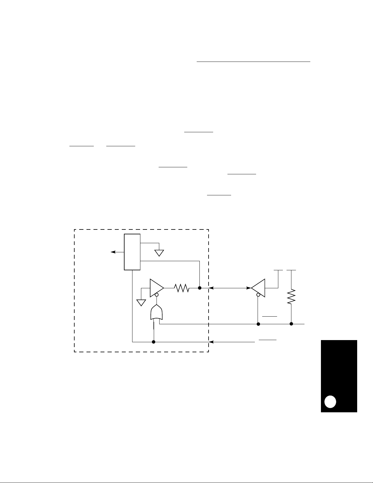
Reset
4.3 HOW TO CONFIGURE RESET
In normal operation, you can configure reset with a hard reset. However, to configure the
development port you must use a soft reset.
4.3.1 Hard Reset
When a hard reset event occurs, the MPC823e reconfigures its hardware system as well as
the development port configuration. The logical value of the bits that determine its initial
mode of operation are sampled either from the data bus or from an internal default constant
(D[0:31]=x’00000000). If, at sampling time, RSTCONF
sampled from the data bus. Otherwise, it is sampled from the internal default. While
HRESET
and RSTCONF are asserted, the MPC823e pulls the data bus low through a weak
resistor (2-4k). You can overwrite this default by driving high to the appropriate bit, as shown
in Figure 4-1. Figures 4-2 through 4-4 illustrate how reset configuration works when
PORESET is asserted. While the PORESET
input signal is being asserted, the core
assumes the default reset configuration that changes when PORESET
CLKOUT signal starts oscillating. In this last case, the hardware configuration is sampled
every nine clock cycles on the rising edge of the CLKOUT. The setup time required for the
data bus is 15 cycles and the maximum rise time of HRESET
cycles. For more information, see Section 4.3.2 Soft Reset .
is asserted, the configuration is
is negated or the
must be less than six clock
MPC823e
CONFIGURATION
WORD
MUX
DX (DATA LINE)
HRESET
RSTCONF
Figure 4-1. Reset Configuration Basic Scheme
RESET
MOTOROLA
MPC823e REFERENCE MANUAL
4
4-7
Page 96
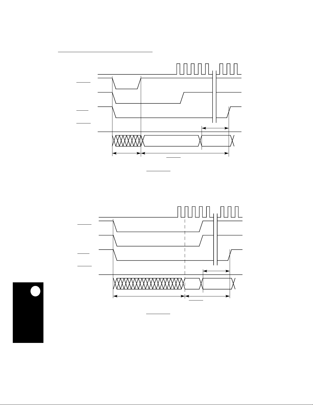
Reset
CLKOUT
PORESET
INTPORESET
HRESET
RSTCONF
D[0:31]
CLKOUT
PORESET
INTPORESET
HRESET
RSTCONF
TSUP
DEFAULT RSTCONF CONTROLLED
Figure 4-2. Reset Configuration Sampling Scheme
For Short PORESET
Assertion
TSUP
4
RESET
4-8
D[0:31]
DEFAULT RSTCONF CONTROLLED
Figure 4-3. Reset Configuration Sampling Scheme
For Long PORESET
MPC823e REFERENCE MANUAL
Assertion
MOTOROLA
Page 97
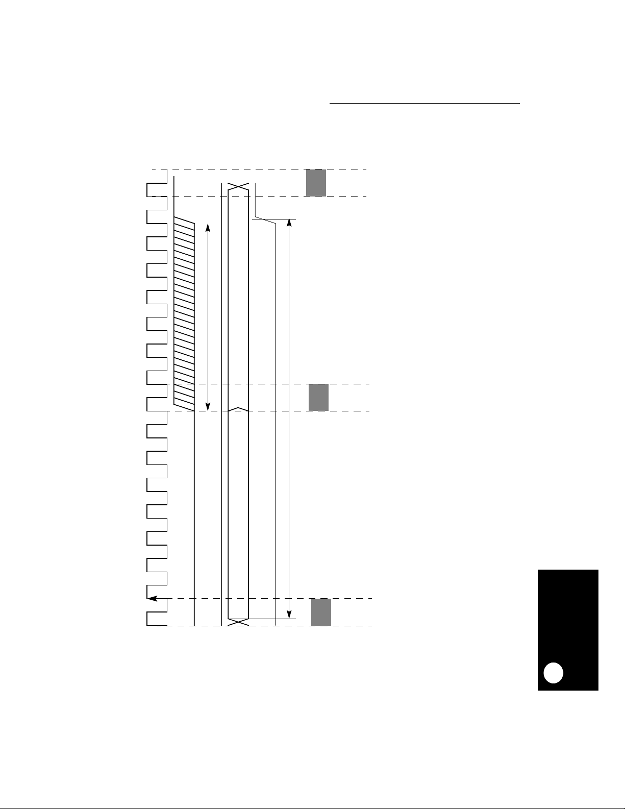
Reset
17
MAXIMUM TIME OF RESET RECOGNITION
DATA
SAMPLE
CONFIGURATION
DATA
SAMPLE
CONFIGURATION
12345678910111213141516
MOTOROLA
CLKOUT
HRESET
RESET CONFIGURATION WORD
RSTCONF
DATA
MPC823e REFERENCE MANUAL
MAXIMUM SETUP TIME OF RESET RECOGNITION
DATA
SAMPLE
Figure 4-4. Reset Configuration Sampling Timing Requirements
CONFIGURATION
RESET
4
4-9
Page 98
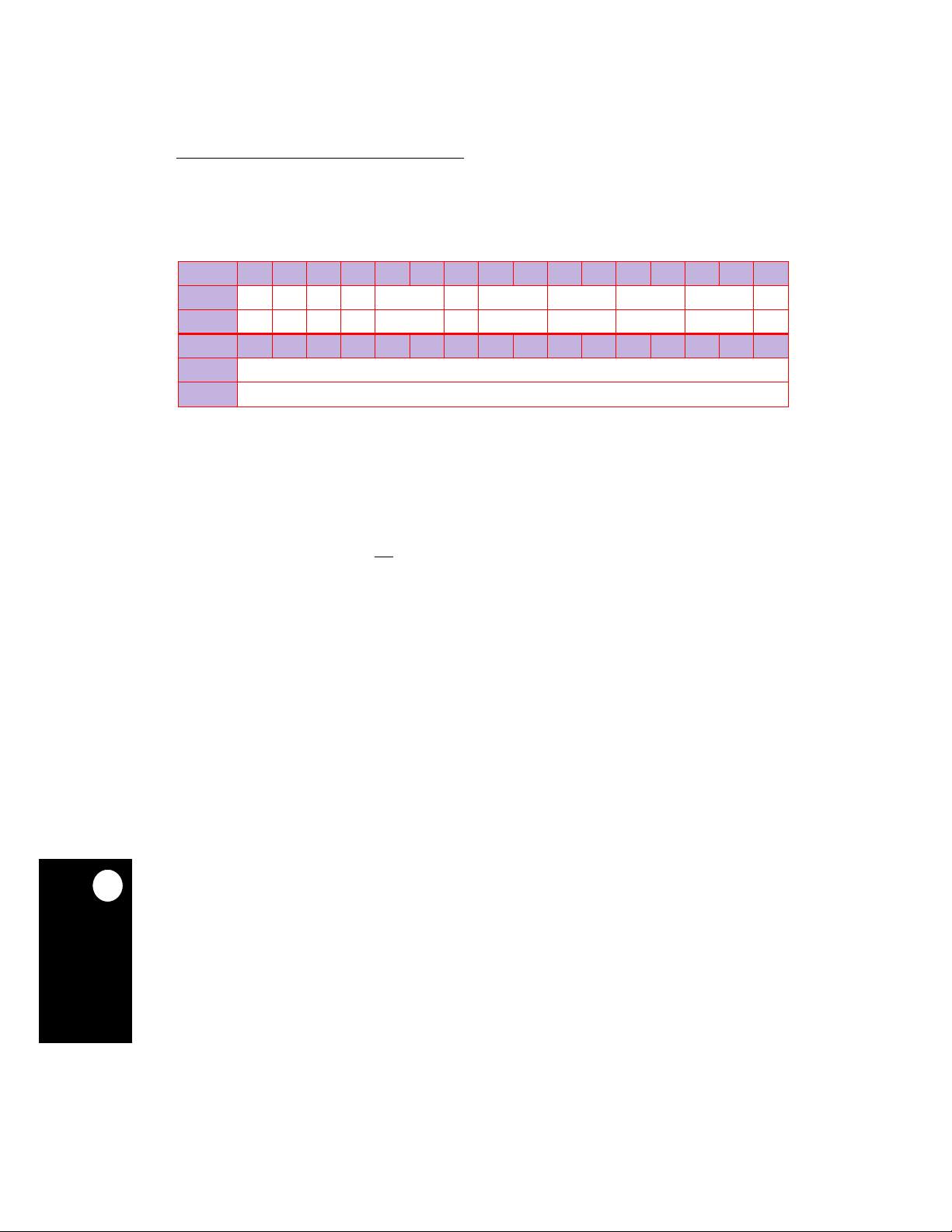
0
Reset
4.3.1.1 HARD RESET CONFIGURATION WORD. The hard reset configuration word is
sampled from the data bus. At reset, the bits will determine the default values of the
corresponding bits in the SIUMCR, IMMR, and MSR.
HARD RESET CONFIGURATION WORD
BIT
FIELD
DEFAULT
BIT
FIELD
DEFAULT
NOTE: The default value is due to the internal pull-down resistor on the data bus.
0 1 2 3 4 5 6 7 8 9 10 11 12 13 14 15
EARB IIP RES BDIS BPS RES ISB DBGC DBPC EBDF RES
00000000000
16 17 18 19 20 21 22 23 24 25 26 27 28 29 30 31
RESERVED
EARB—External Arbitration
If this bit is set (1), external arbitration is assumed. If it is cleared (0), then internal arbitration
is performed. See Section 12 System Interface Unit for more information.
4
RESET
IIP—Initial Interrupt Prefix
This bit defines the initial value of the MSR
the interrupt table location. If IIP
sampled one, the MSR
initial value is zero.
IP
is zero (default), the MSR
immediately after reset. The MSR
IP
initial value is one, but if it is
IP
Bits 2, 6, and 15—Reserved
These bits are reserved and must be left open.
BDIS—Boot Disable
0 = The memory controller is activated after reset so that it matches all addresses.
1 = The memory controller is not activated after reset, but it is cleared.
BPS—Boot Port Size
This field defines the port size of the boot device.
00 = 32-bit port size.
01 = 8-bit port size.
10 = 16-bit port size.
11 = Reserved.
bit defines
IP
4-10
MPC823e REFERENCE MANUAL
MOTOROLA
Page 99

Reset
ISB—Initial Internal Space Base Select
This field defines the initial value of the IMMR bits 0-15 and determines the base address of
the internal memory space. Make sure that the IMMR is not in the interrupt address space
(IIP).
00 = 0x00000000.
01 = 0x00F00000.
10 = 0xFF000000.
11 = 0xFFF00000.
DBGC—Debug Pins Configuration
This field configures the functionality of the following pins.
00 = IP_B[0:1]/IWP[0:1]/VFLS[0:1] functions as IP_B[0:1].
IP_B3/IWP2/VF2 functions as IP_B3.
IP_B4/LWP0/VF0 functions as IP_B4.
IP_B5/LWP1/VF1 functions as P_B5.
OP2/MODCK1/STS
functions as OP2.
ALE_B/DSCK/AT1 functions as ALE_B.
IP_B2/AT2 functions as IP_B2.
IP_B6/DSDI/AT0 functions as IP_B6.
IP_B7/PTR
/AT3 functions as IP_B7.
OP3/MODCK2/DSDO functions as OP3.
01 = IP_B[0:1]/IWP[0:1]/VFLS[0:1] functions as IWP[0:1].
IP_B3/IWP2/VF2 functions as IWP2.
IP_B4/LWP0/VF0 functions as LWP0.
IP_B5/LWP1/VF1 functions as LWP1.
OP2/MODCK1/STS functions as STS
.
ALE_B/DSCK/AT1 functions as AT1.
IP_B2/AT2 functions as AT2.
IP_B6/DSDI/AT0 functions as AT0.
IP_B7/PTR
/AT3 functions as AT3.
OP3/MODCK2/DSDO functions as OP3.
10 = Reserved.
11 = IP_B[0:1]/IWP[0:1]/VFLS[0:1] functions as VFLS[0:1].
IP_B3/IWP2/VF2 functions as VF2.
IP_B4/LWP0/VF0 functions as VF0.
IP_B5/LWP1/VF1 functions as VF1.
OP2/MODCK1/STS functions as STS
.
ALE_B/DSCK/AT1 functions as AT1.
IP_B2/AT2 functions as AT2.
IP_B6/DSDI/AT0 functions as AT0.
IP_B7/PTR
/AT3 functions as AT3.
OP3/MODCK2/DSDO functions as OP3.
MOTOROLA
MPC823e REFERENCE MANUAL
RESET
4
4-11
Page 100

Reset
DBPC—Debug Port Pins Configuration
This field configures the following pins on the active development port.
00 = ALE_B/DSCK/AT1 functions as defined by DBGC.
IP_B6/DSDI/AT0 functions as defined by DBGC.
OP3/MODCK2/DSDO functions as defined by DBGC.
IP_B7/PTR
/AT3 functions as defined by DBGC.
TCK/DSCK functions as DSCK.
TDI/DSDI functions as DSDI.
TDO/DSDO functions as DSDO.
01 = ALE_B/DSCK/AT1 functions as defined by DBGC.
IP_B6/DSDI/AT0 functions as defined by DBGC.
OP3/MODCK2/DSDO functions as defined by DBGC.
IP_B7/PTR
/AT3 functions as defined by DBGC.
TCK/DSCK functions as TCK.
TDI/DSDI functions as TDI.
TDO/DSDO functions as TDO.
10 = Reserved.
11 = ALE_B/DSCK/AT1 functions as DSCK.
IP_B6/DSDI/AT0 functions as DSDI.
OP3/MODCK2/DSDO functions as DSDO.
IP_B7/PTR
/AT3 functions as PTR.
TCK/DSCK functions as TCK.
TDI/DSDI functions as TDI.
TDO/DSDO functions as TDO.
4
RESET
EBDF—External Bus Division Factor
These bits define the frequency division factor between GCLK1/GCLK2 and
GCLK1_50/GCLK2_50. CLKOUT is similar to GCLK2_50. GCLK2_50 and GCLK1_50 are
used by the system interface unit and memory controller to interface with the external
system. The EBDF bits (described in Section 5.2.1 System Clock and Reset Control
Register ) are initialized during HRESET
using the hard reset configuration mechanism.
4.3.2 Soft Reset
When a soft reset event occurs, the MPC823e reconfigures the development port.
4-12
MPC823e REFERENCE MANUAL
MOTOROLA
 Loading...