

Page 1

Freescale Semiconductor, Inc.
MPC564EVB User’s Manual
nc...
I
cale Semiconductor,
Frees
MPC564EVBUM
Rev. 1.2, 3/2003
For More Information On This Product,
Go to: www.freescale.com
Page 2

Revision History
Freescale Semiconductor, Inc.
Version
Number
1.1 11/2002 Initial Version
1.2 3/2003 Fixed typos. Added appendix describing dBUG ethernet configu-
nc...
I
cale Semiconductor,
Revision
Date
Description of Changes
ration. Added appendix for emulating the MPC53X parts. Added
66MHz references.
Frees
For More Information On This Product,
Go to: www.freescale.com
Page 3

Freescale Semiconductor, Inc.
DigitalDNA and Mfax are trademarks of Motorola, Inc.
IBM PC and IBM AT are registered trademark of IBM Corp.
All other trademark names mentioned in this manual are the registered trade mark of respective owners
nc...
I
No part of this manual and the dBUG software provided in Flash ROM’s/EPROM’s may be reproduced, stored in a retrieval system, or
transmitted in any form or by any means, electronic, mechanical, photocopying, recording, or otherwise. Use of the program or any
part thereof, for any purpose other than single end user by the purchaser is prohibited.
cale Semiconductor,
Frees
Motorola reserves the right to make changes without further notice to any products herein. Motorola makes no warranty,
representation or guarantee regarding the suitability of its products for any particular purpose, nor does Motorola assume any liability
arising out of the application or use of any product or circuit, and specifically disclaims any and all liability, including without limitation
consequential or incidental damages. “Typical” parameters which may be provided in Motorola data sheets and/or specifications can
and do vary in different applications and actual performance may vary over time. All operating parameters, including “Typicals” must
be validated for each customer application by customer’s technical experts. Motorola does not convey any license under its patent
rights nor the rights of others. Motorola products are not designed, intended, or authorized for use as components in systems
intended for surgical implant into the body, or other applications intended to support or sustain life, or for any other application in
which the failure of the Motorola product could create a situation where personal injury or death may occur. Should Buyer purchase or
use Motorola products for any such unintended or unauthorized application, Buyer shall indemnify and hold Motorola and its officers,
employees, subsidiaries, affiliates, and distributors harmless against all claims, costs, damages, and expenses, and reasonable
attorney fees arising out of, directly or indirectly, any claim of personal injury or death associated with such unintended or
unauthorized use, even if such claim alleges that Motorola was negligent regarding the design or manufacture of the part. Motorola
and are registered trademarks of Motorola, Inc. Motorola, Inc. is an Equal Opportunity/Affirmative Action Employer.
How to reach us:
USA/EUROPE/Locations Not Listed: Motorola Literature Distribution; P.O. Box 5405, Denver, Colorado 80217. 1–303–675–2140
or 1–800–441–2447
JAPAN: Motorola Japan Ltd.; SPS, Technical Information Center, 3–20–1, Minami–Azabu. Minato–ku, Tokyo 106–8573 Japan.
81–3–3440–3569
ASIA/PACIFIC: Motorola Semiconductors H.K. Ltd.; Silicon Harbour Centre, 2 Dai King Street, Tai Po Industrial Estate, Tai Po, N.T.,
Hong Kong. 852–26668334
Technical Information Center: 1–800–521–6274
HOME PAGE: http://www.motorola.com/s emiconductors
Document Comments: FAX (512) 895-2638, Attn: RISC Applications Engineering
World Wide Web Addresses: http://www.motorola.com/PowerPC
http://www.motorola.com/NetComm
http://www.motorola.com/ColdFire
Axiom Manufacturing: http://www.axman.com
For More Information On This Product,
Go to: www.freescale.com
© Motorola Inc., 2002. All rights reserved.
Page 4

Freescale Semiconductor, Inc.
Cautionary Notes
Axiom Manufacturing (http://www.axman.com) reserves the right to make changes without
further notice to any products to improve reliability, function or design. Axiom does not
assume any liability arising out of the application or use of any product or circuit described
herein; neither does it convey any license under patent rights or the rights of others. Axiom
products are not designed, intended, or authorized for use as components in systems
intended for surgical implant into the body, or other applications intended to support or sustain life, or for any other application in which failure of the Axiom product could create a
situation where personal injury or death may occur. Should Buyer purchase or use Axiom
manufacturing products for any such unintended or unauthorized application, Buyer shall
indemnify and hold Axiom Manufacturing and its officers, employees, subsidiaries, affiliates, and distributors harmless against all claims, costs, damages, and expenses, and reasonable attorney fees arising out of, directly or indirectly, any claim of personal injury or death
associated with such unintended or unauthorized use, even if such claim alleges that Axiom
nc...
I
Manufacturing was negligent regarding the design or manufacture of the part or system.
cale Semiconductor,
Frees
EMC Information on MPC564EVB
1. This product as shipped from the factory with associated power supplies and cables,
has been tested and meets with requirements of EN5022 and EN 50082-1: 1998 as a
CLASS A product.
2. This product is designed and intended for use as a development platform for hardware or software in an educational or professional laboratory.
3. In a domestic environment this product may cause radio interference in which case
the user may be required to take adequate measures.
4. Anti-static precautions must be adhered to when using this product.
5. Attaching additional cables or wiring to this product or modifying the products operation from the factory default as shipped may effect its performance and also cause
interference with other apparatus in the immediate vicinity. If such interference is
detected, suitable mitigating measures should be taken.
For More Information On This Product,
Go to: www.freescale.com
Page 5

Freescale Semiconductor, Inc.
WARNING
This board generates, uses, and can radiate radio frequency energy and, if not installed
properly, may cause interference to radio communications. As temporarily permitted by
regulation, it has not been tested for compliance with the limits for class a computing devices
pursuant to Subpart J of Part 15 of FCC rules, which are designed to provide reasonable
protection against such interference. Operation of this product in a residential area is likely
to cause interference, in which case the user, at his/her own expense, will be required to
correct the interference.
nc...
I
cale Semiconductor,
Frees
For More Information On This Product,
Go to: www.freescale.com
Page 6

Freescale Semiconductor, Inc.
nc...
I
cale Semiconductor,
Frees
For More Information On This Product,
Go to: www.freescale.com
Page 7

Freescale Semiconductor, Inc.
Contents
nc...
I
cale Semiconductor,
Frees
Paragraph
Number Title
Chapter 1
MPC564 EVB Board
1.1 Processor.............................................................................................................. 1-3
1.2 System Memory................................................................................................... 1-4
1.2.1 External Flash.................................................................................................. 1-4
1.2.2 SRAM.............................................................................................................. 1-5
1.2.3 Internal SRAM................................................................................................. 1-5
1.2.4 Internal Flash ...................................................................................................1-5
1.2.5 MPC564EVB Memory Map............................................................................ 1-5
1.2.5.1 Memory Device / Bank Selection and Configuration.................................. 1-6
1.2.5.2 Memory Bank Chip Select Configuration................................................... 1-7
1.2.5.3 Reset Vector Mapping..................................................................................1-7
1.3 Support Logic ...................................................................................................... 1-8
1.3.1 Reset Logic...................................................................................................... 1-8
1.3.2 Clock Circuitry ................................................................................................1-8
1.3.3 Watchdog Timer...............................................................................................1-8
1.3.4 Exception Sources............................................................................................ 1-9
1.3.5 TA Generation.................................................................................................. 1-9
1.3.6 User’s Program................................................................................................ 1-9
1.3.7 Power Oak K/I/S Hardware Options ............................................................. 1-10
1.4 Communication Ports ........................................................................................ 1-11
1.4.1 COM1 and COM2 ......................................................................................... 1-11
1.4.2 CAN PORTs and Options ..............................................................................1-12
1.4.3 10/100T Ethernet Port.................................................................................... 1-14
1.4.4 BDM and NEXUS Development Ports .........................................................1-15
1.4.4.1 BDM Port Options..................................................................................... 1-15
1.4.4.2 Nexus Connector ....................................................................................... 1-16
1.5 Connectors and User Components..................................................................... 1-19
1.5.1 Keypad...........................................................................................................1-19
1.5.2 LCD Port........................................................................................................ 1-19
1.5.3 User Components........................................................................................... 1-21
1.5.4 MPC564EVB Hardware Options................................................................... 1-21
1.5.5 Signals Available on Board............................................................................ 1-22
1.5.5.1 IRQ PORT ................................................................................................. 1-22
1.5.5.2 BUS_PORT................................................................................................ 1-22
1.5.5.3 TPU_PORTs .............................................................................................. 1-23
1.5.5.4 CONTROL_PORT .................................................................................... 1-24
1.5.5.5 MIOS_PORT .............................................................................................1-25
1.5.5.6 QADC_PORTs........................................................................................... 1-26
1.5.5.7 QSM_PORT............................................................................................... 1-27
1.5.5.8 MICTOR 1 – 3 PORTs...............................................................................1-27
Page
Number
MOTOROLA MPC564EVB User’s Manual i
For More Information On This Product,
Go to: www.freescale.com
Page 8

Freescale Semiconductor, Inc.
Contents
nc...
I
cale Semiconductor,
Frees
Paragraph
Number Title
1.6 Reference Documents........................................................................................ 1-28
1.7 Software Development ...................................................................................... 1-28
Chapter 2 Initialization and Setup
2.1 System Configuration .......................................................................................... 2-1
2.2 Installation And Setup ......................................................................................... 2-3
2.2.1 Unpacking........................................................................................................ 2-3
2.2.2 Preparing the Board for Use ............................................................................2-3
2.2.3 Providing Power to the Board.......................................................................... 2-3
2.2.4 Selecting Terminal Baud Rate .........................................................................2-5
2.2.5 The Terminal Character Format.......................................................................2-5
2.2.6 Connecting the Terminal.................................................................................. 2-5
2.2.7 Using a Personal Computer as a Terminal....................................................... 2-5
2.3 MPC564EVB Jumper and Switch Setup............................................................. 2-6
2.3.1 Reset Configuration Word and Configuration Switch (CONFIG_SW) ..........2-8
2.3.2 Memory Configuration (MAP_SW).............................................................. 2-10
2.4 System Power-up and Initial Operation............................................................. 2-10
Chapter 3
Using the Monitor/Debug Firmware
3.1 What Is dBUG?.................................................................................................... 3-1
3.2 Operational Procedure .........................................................................................3-2
3.2.1 System Power-up............................................................................................. 3-2
3.2.2 System Initialization........................................................................................ 3-4
3.2.2.1 Hard RESET Button.................................................................................... 3-5
3.2.2.2 Non-Maskable Interrupt Button................................................................... 3-5
3.2.2.3 Software Reset Command. ..........................................................................3-5
3.3 Command Line Usage ......................................................................................... 3-6
3.4 Commands ........................................................................................................... 3-6
3.5 System Call Functions....................................................................................... 3-39
3.5.1 OUT_CHAR.................................................................................................. 3-39
3.5.2 IN_CHAR...................................................................................................... 3-39
3.5.3 IN_STAT........................................................................................................ 3-40
3.5.4 ISR_REGISTER............................................................................................ 3-40
3.5.5 ISR_REMOVE ..............................................................................................3-40
3.5.6 EXIT_TO_dBUG........................................................................................... 3-41
Page
Number
Appendix A
MPC533/534 Emulation
ii MPC564EVB User’s Manual MOTOROLA
For More Information On This Product,
Go to: www.freescale.com
Page 9

Freescale Semiconductor, Inc.
Contents
Paragraph
Number Title
Appendix B
Configuring dBUG for Network Downloads
B.1 Required Network Parameters.............................................................................B-1
B.2 Configuring dBUG Network Parameters.............................................................B-1
B.3 Troubleshooting Network Problems....................................................................B-2
nc...
I
cale Semiconductor,
Page
Number
Frees
MOTOROLA MPC564EVB User’s Manual iii
For More Information On This Product,
Go to: www.freescale.com
Page 10

Freescale Semiconductor, Inc.
Contents
Paragraph
Number Title
nc...
I
cale Semiconductor,
Page
Number
Frees
iv MPC564EVB User’s Manual MOTOROLA
For More Information On This Product,
Go to: www.freescale.com
Page 11

Freescale Semiconductor, Inc.
Chapter 1
MPC564 EVB Board
The MPC564EVB is an MPC564-based evaluation board that can be used for the development and
test of microcontroller systems1 (see Figure 1-1). The MPC564 is a member of the Motorola
MPC500 RISC microcontroller family. It is a 32-bit processor with a 32-bit internal address bus
and 32 lines of data.
The evaluation board is a development and test platform for software and hardware for the
nc...
I
cale Semiconductor,
Frees
MPC5641. The system provides for development of target applications for the similar MPC561,
MPC562, or MPC563 microcontrollers also. It can be used by software and hardware developers
to test programs, tools, or circuits without having to develop a complete microcontroller system
themselves. All special features of the MPC5641 are supported.
The heart of the evaluation board is the MPC564. The MPC564EVB has 512Kbyte (128K x 32)
external SRAM for development or application memory, 2Mbyte (512K x 32) external Flash
memory, and numerous hardware expansion possibilities. The MPC564EVB board also provides
an Ethernet interface (10/100BaseT), T ouCAN, and RS232 interface in addition to the built-in I/O
functions of the MPC564
cessor. To support development and test, the evaluation board can be connected to debuggers and
emulators produced by different manufacturers.
The MPC564EVB provides for low cost software testing with the use of a ROM resident debug
monitor, dBUG, programmed into the external Flash device. Operation allows the user to load
code in the on-board RAM, execute applications, set breakpoints, and display or modify registers
or memory. After software is operational, the user may program the MPC564 Internal Flash
EEPROM or the on-board FLASH memory for dedicated operation of new software application.
No additional hardware or software is required for basic operation. For high level debug, extensive third-party tools are available for the MPC500 series. The Nexus and BDM debug ports are
available to connect the tool sets.
1
device for programming and evaluating the attributes of the micropro-
Specifications
1
Clock: 66 MHz Maximum
Operating temperature: 0°C to +70°C
Power requirement: 6 – 26V DC @ 300 ma Typical
Power output: 5.8V @ 1.5A output with 5V, 3.3V, and 2.6V regulated supplies
Board Size: 7.00 x 7.60 inches, 8 layers
1
The MPC564EVB can be used to emulate the MPC533 and MPC534. See Appendix A and MPC564CZP66
Electrical Spec for limitations.
, 4Mhz reference
Chapter 1. MPC564 EVB Board 1-1
For More Information On This Product,
Go to: www.freescale.com
Page 12

Freescale Semiconductor, Inc.
•Memory Devices:
512K Byte (128K x 32) Sync. SRAM, optional additional 512K Byte
2M Byte (512K x 32) Sync. FLASH
512K Byte FLASH internal to MPC564 device
32K Byte SRAM internal to MPC564 device
•POWER OAK (PC33394 P2.6) regulated power supply for 5V, 3.3V and 2.6V supplies.
•MAP Switch – provides easy assignment of chip selects and memory mapping.
•CONFIG Switch – Basic necessary Reset Word Configuration options.
•COM1 - SCIA1 with RS232 type DB9-S Connection
•COM2 - SCIA2 with RS232 type DB9-S Connection, TX / RX polarity option.
•CAN Ports
•10/100T Ethernet Port – LAN91C111 based MAC+PHY, memory mapped.
•DEVELOPMENT Ports – Nexus 50 pin and dual voltage BDM Port.
•LCD Port - LCD Module Interface Connector w/ Contrast Adjust, Buffered and Memory
nc...
I
Mapped
•KEYPAD Port
•BUS Port – 32 data and 24 address lines on 60 pin header.
•CONTROL Port - Bus Controls with 40 pin header.
•QSM Port – Serial I/O port with 16 pin socket header.
•MIOS Port - MDA, PWM, and MGPIO ports with 34 pin socket header.
1
– 3 CAN transceiver interfaced ports, 1 x 4 headers.
1
- 16 Key passive interface, applies QADC_B channels for operation.
cale Semiconductor,
Frees
•TPU Ports1 - 2 Timing Processor I/O ports with 20 pin socket headers.
•QADC Ports1 - 2 Analog I/O ports, one 20 pin and one 24 pin socket header.
•IRQ Port – Interrupt or MPC564 port I/O with 10 pin socket header.
•POWER Port – Primary and standby power supply access port, no header.
•I/O Connecto rs in .1 g rid, pin headers for bus and control provide easy ribbon cable connection
for external connections. Socket headers provide easy wire connection to breadboard prototype
area with 22ga solid wire.
•Large Prototyping Area with +5V and ground connection grids.
•Mictor Logic Probe connectors for the Address and Data bus (Not installed default)
•Breadboard Prototyping area (2.5 x 1.5 inch) for easy installation of test connections.
•System Indicators – Reset Indicator, Supply voltage indications for 5V, 3.3V, and 2.6V supplies
•Reset Switches – POReset, Hard, Soft reset buttons.
•User Components – 4 user LEDs (one with debounce), 4 user Switches, 1 user Potentiometer
with socket header for I/O connection.
1
The MPC533/4 has limited or no functionality for this module. See Appendix A
1-2 MPC564EVB User’s Manual
For More Information On This Product,
Go to: www.freescale.com
Page 13

Freescale Semiconductor, Inc.
nc...
I
Processor
cale Semiconductor,
Frees
Figure 1-1. M PC 564EVB top view
1.1 Processor
The microprocessor used on the MPC564EVB is the highly integrated Motorola PowerPC
MPC564 32-bit microcontroller . The MPC564 i mplements a PPC ISA core with 512KByte UC3F
flash, two UART channels, two Timing Processor Units (TPUs)1, 32 KBytes of SRAM, a QSPI
(Queued Serial Peripheral Interface) module, three TouCAN modules
submodules in the MIOS, enhanced QADC64E, PPM module
8KByte DPTRAM1. This processor communicates with external devices over a 32-bit wide data
bus, D[0:31]. The MPC564 can address a 32 bit address range. Only 24 bits are available on the
bus however . There are inte rnally generated chip sele cts to allow the full 3 2 bit address range to be
selected. There are regions that can be decoded to allow superviser, user , instruction, and data each
to have the 32-bit address range. All the processor’s signals are available through the expansion
connector (BUS_PORT). Refer to the schematic for their pin assignments.
The MPC564 processor has the capability to support both an IEEE-ISTO 5001-1999 NEXUS port
and a BDM debug port. These ports are multiplexed and can be used with third party tools to allow
the user to download code to the board. The board is configured to boot up in the normal/BDM
mode of operation. The BDM signals are available at the port labeled BDM_PORT. The NEXUS
connector is near the reset switches on the board. It is the 2002 50 pin standard I/O connections and
connector. The BDM and NEXUS ports can not be used at the same time.
1
, a Nexus debug interface port, and
1
, 12 PWMs and 6 counter
1
The MPC533/4 has limited or no functionality for this module. See Appendix A.
MPC564EVB User’s Manual 1-3
For More Information On This Product,
Go to: www.freescale.com
Page 14

System Memory
Freescale Semiconductor, Inc.
Figure 1-2 shows the MPC564 block diagram.
nc...
I
cale Semiconductor,
Frees
JTAG
Burst
Buffer
Controller 2
DECRAM
(2Kbytes)
MPC500
Core
+
FPU
32K CALRAM
28 Kbytes
4-Kbyte Overlay
QADC64E
TPU3
QADC64E
8-Kbyte
DPTRAM
Figure 1-2. MPC564
1.2 System Memory
L-BUS
TPU3
512 Kbytes
Nexus
QSMCM
Flash*
U-BUS
L2U
PPM
Tou
CAN
1
Tou
CAN
Block Diagram
UIMB
Tou
CAN
USIU
MIOS14
IMB3
E-BUS
1.2.1 External Flash
One on-board Flash ROM (U4) is used in the system. The Am29BDD160G device contains
16Mbits of non-volatile storage (1 M x 16-bit/512 K x 32-bit) giving a total of 2MBytes of Flash
memory. This device requires a 32 bit wide port and must be written in 32 bit word size data. It
may be read in bytes, half words, or words. W ait states are required to access in asynchronous mode
and the same wait state delay is required during the first cycle of a burst type access. Refer to the
specific device data sheet for configuring the flash memory. User should note that the debug
monitor firmware is installed in this flash device. Development tools or user application programs
1
See Appendix A for block diagram of MPC533/4
1-4 MPC564EVB User’s Manual
For More Information On This Product,
Go to: www.freescale.com
Page 15

Freescale Semiconductor, Inc.
may erase or corrupt the debug monitor. If the debug monitor becomes corrupted and it’s operation
is desired, the firmware must be programmed into the flash by applying a development port tool
such as BDM or Nexus. User should use caution to avoid this situation. The upper 1 MByte is used
to store the MPC564EVB dBUG debugger/monitor firmware (0x0090_0000 to 0x009F_FFFF).
System Memory
1.2.2 SRAM
The MPC564EVB has one 512 KByte device on the board (U2). It’s starting address is
0xFFF0_0000.
The synchronous SRAM Memory Bank is composed of one (optional 2) 128K x 32 memory
devices. These memory devices are connected in linear order from U2 to U3 if more than one is
available, so that the low order address of the memory bank will access U2 and the high order
addresses of the memory bank will access U3. This memory bank must be configured as a 32 bit
wide port but is byte, half word, and word accessible for read or write operations.
nc...
I
cale Semiconductor,
Frees
Also see Section 1.2.5, “MPC564EVB Memory Map”.
1.2.3 Internal SRAM
The MPC564 processor has 32-KBtyes of internal memory which may be used as data or
instruction memory . This memory is mapped to 0x003F_8000 and configured as data space but is
not used by the dBUG monitor except during system initialization. After system initialization is
complete, the internal memory is availabl e to the user . The memory is relocatabl e to any 32-KByte
boundary.
1.2.4 Internal Flash
The MPC564 has a U-bus CDR3 flash EEPROM module (UC3F). The primary function of the
UC3F flash EEPROM module is to serve as electrically programmable and erasable non-volitle
memory (NVM) to store program instructions and/or data. The MPC564 flash EEPROM array has
512 Kbytes of NVM that is divided into eight 64-Kbyte array blocks. If the flash array is disabled
in the IMMR register (FLEN=0), then neither the UC3F array or the UC3F control registers are
accessible. This feature allows the MPC564 to emulate the MPC561/562.
Please refer to the MPC564 User’s Manual for more details.
NOTE:
The internal flash can not be programmed at 66MHz. Please see the
MPC564CZP66 Electrical Spec for other limitations at 66MHz.
1.2.5 MPC564EVB Memory Map
Interface signals to support interface to external memory and peripheral devices are generated by
the memory controller. It supports four regions on four chip-select pins. The general purpose
chip-selects are available on lines CS[0] through CS[3]. CS[0] also functions as the global (boot)
chip-select for booting out of external flash.
MPC564EVB User’s Manual 1-5
For More Information On This Product,
Go to: www.freescale.com
Page 16

System Memory
Freescale Semiconductor, Inc.
Since the MPC564 chip selects are fully programmable, the memory banks can be located at any
location in the MPC5xx memory space.
Following is the default memory map for this board as configured by the Debug Monitor located
in the external flash bank. The internal memory space of the MPC564 is detailed further in the
MPC561/3 Users Manual. Chip Selects 0-3 can be changed by user software to map the external
memory in different locations but the chip select configuration such as wait states and transfer
acknowledge for each memory type should be maintained.
Possible Chip Select usage:
Synchronous SRAM Memory Bank CS0 or CS1 default CS1, MAP SW. 1,2
Synchronous FLASH Memory Bank CS0 or CS2 default CS0, MAP SW. 3,4
10/100T / LCD Port CS3 default CS3, MAP SW. 6,7
MPC564 Internal Flash N/A MAP_SW. 8, may effect mem-
nc...
I
ory map of chip selects
The MPC564EVB Default Memory Map shows the MPC564EVB memory map.
cale Semiconductor,
Frees
Table 1-1. The MPC564EVB Default Memory Map
Address Range Signal and Device
0x0000_0000 - 0x0007_FFFF 512KByte UC3F Flash
0x0008_0000 - 0x002F_7FFF Reserved for Flash
0x002F_8000 - 0x002F_87FF BBC DECRAM 2 KBytes
0x002F_8800 - 0x002F_9FFF Reserved for BBC
0x002F_A000 - 0x002F_BFFF BBC Control
0x002F_C000 - 0x002F_FFFF USIU & Flash Control
0x0030_0000 - 0x0030_7FFF UIMB I/F & IMB Modules 32KBytes
0x0030_8000 - 0x0037_FFFF Reserved for IMB
0x0038_0000 - 0x0038_007F CALRAM/READI Control
0x0038_0080 - 0x0038_3FFF Reserved (L-bus Control)
0x0038_4000 - 0x003F_7FFF Reserved (L-bus Memory)
0x003F_8000 - 0x003F_FFFF CALRAM (internal SRAM)
0x0080_0000 - 0x00A0_0000 External Flash 2MByte (0x0090_0000 -
0x00A0_0000 reserved for dBUG)
0x0100_0000 - 0x0108_0000 Ethernet
0xFFF0_0000 - 0xFFF8_0000 External SRAM 512KByte
1.2.5.1 Memory Device / Bank S electio n and C onfigur ation.
The MPC564EVB board has two internal memory banks, two external memory banks and a
Peripheral memory bank that provide:
1-6 MPC564EVB User’s Manual
For More Information On This Product,
Go to: www.freescale.com
Page 17

Freescale Semiconductor, Inc.
x 32KByte Internal SRAM
MPC564 512K byte Internal FLASH Memory (U1)
x
x 128K x 32bit (512KByte) Synchronous Static RAM (U2), 1M Byte with U3 option.
x 512K x 32bit (2MByte) Synchronous Flash EEPROM (U4)
x Peripherals 10/100T Ethernet and LCD Port
System Memory
Each external RAM or Flash memory bank can be configured individually to operate from the
MPC564 chip selects. Caution should be used not to place more than one memory bank on the CS0
chip select and to properly configure the chip select to control the memory devices provided in the
memory bank correctly. Failur e to observe precautions may r ender the external memory bus
inoperable.
The MAP Switch (MAP_SW) connects MPC564 chip selects to the different external memory
banks. If memory access problems occur, the settings of these options and the associated chip
select configurations should be reviewed with some detail. Information to configure the chip
selects and memory is detailed in the following section.
nc...
I
1.2.5.2 Memory Bank Chi p Selec t Confi guration
cale Semiconductor,
Frees
Application software that executes on Reset must configure each memory bank chip select
properly for correct operation. Chip Select Memory Options shows the default memory settings
programmed by the dBUG ROM monitor and may be applied for most user applications:
Table 1-2. Chip Select Memory Options
Memory Bank Reg. Default Value Notes
CS1 = SRAM BR1 0xFFF0_0003 Base Address = 0xFFF0_0 000 , Port wi d th = 32 bit *Default
CS1 = SRAM, asynchr o-
nous access mode
CS0 = FLASH BR0 0x0080_0003 Base address 0x0080_0000, Port width = 32 bit *Default
CS0 = FLASH, asynchro-
nous access mode
CS3 = Peripheral BR3 0x0100_0807 Base address = 0x0100_0000, Po rt w id t h = 16 bit *Default
OR1 0xFFF0_0000 Memory Range = 0xFFF0_0 000 > 0xFFF7_ FFFF, wait state
= 0. Note U2 = 512K bytes and will mirror 4x with this setting. Usable range = 0xFFF0_8000 – 0xFFF7_FFFF.
OR0 0xFFE0_0030 Memory range = 0x0080_0000 > 0x009F_FFFF, wait state
= 3, asynchronous operation 40Mhz clock, 95ns device.
Note U4 = 2M bytes and will mirror 2x with this setting.
Usable range = 0x00 80_ 0000 > 0x008F_FFFF (dBUG m on itor is in upper half starting at 0x00 90_ 0000)
External TA* generation provided.
CS3 = Peripheral, asynchronous
OR3 0xFFFF_80F0 Memory Range 0x0100_0000 > 0100_7FFF, wait state =
External Terminate (T A*) *Default Note Peripher al mem ory
map.
1.2.5.3 Reset Vector Mapping
After reset, the processor attempts to execute at physical address 0x0000_0100 if the hard reset
configuration word IP bit is cleared to 0 or physical address 0xFFF0_0100 if the hard reset
MPC564EVB User’s Manual 1-7
For More Information On This Product,
Go to: www.freescale.com
Page 18

Freescale Semiconductor, Inc.
Support Logic
configuration word IP bit is set to 1. This requires the board to have a non-volatile memory device
in this range with the correct information stored in it. The MPC564 processor chip-select zero
(CS0
) responds to any accesses after reset until the OR0 is written. Since CS0 (the global chip
select) is connected to the Flash ROM (U6), the Flash ROM initially appears at address
0xFFF0_0000. The initialization routine then programs the chip-select logic, locates the Flash
ROM to start at 0x0080_0000 and configures the rest of the internal and external peripherals.
Please refer to the MPC561/563 user’s manual (Global (Boot) Chip-Select Operation) for more
information.
1.3 Support Logic
1.3.1 Reset Logic
nc...
I
cale Semiconductor,
Frees
The reset logic provides system initialization. Reset occurs during power-on or via assertion of the
signal RESET which causes the MPC564 to reset. HRESET is triggered by the reset switch (SW1)
which resets the entire processor/system.
dBUG configures the MPC564 microprocessor internal resources during initialization. The
contents of the exception table are copied to address 0xFFF0_0000 in the SDRAM. The Software
W atchdog Timer is disabled, the Bus Monitor is enabled, and the internal timers are placed in a stop
condition. A memory map for the entire board can be seen in Table 1-1., “The MPC564EVB
Default Memory Map”.
RW0 – 30: External Reset Configuration Word (RCW) Options
R W0, RW2, RW4 – 18, RW23 – 30 provide the user access to external Reset Configuration Word
(RCW) bits not normally required for default MPC564EVB operation. The RW0 – 30 designations
reflect the data bus D0 – D30 bit effected when the RCW word is enabled externally. All RW0 –
30 option bits are defaulted to the logic low value during external RCW word operation. The user
may apply a wire jumper between the 2 pad positions of each RW0 – 30 option to provide a logic
high level on the respective bit position during external RCW operation. Refer to the MPC564 user
manual Reset chapter for the respective RCW bit definitions.
1.3.2 Clock Circuitry
The MPC564EVB board uses a 4MHz crystal (Y1 on the schematics) to provide the clock to the
on-chip oscillator of the MPC564. In addition to the 4MHz crystal, there is also a 25MHz oscillator
(Y3) which feeds the Ethernet chip (U20).
1.3.3 Watchdog Timer
The duration of the Watchdog is selected by the SWT[1:0] bits in the System Protection and
Control Register (SYPCR), SWT[1:0] = 0b11 gives a maximum timeout period of 228/System
frequency. The dBUG monitor initializes these bits with the value 0b11, which provides the
maximum time-out period, but dBUG does NOT enable the watchdog timer via the SYPCR
register SWE bit.
1-8 MPC564EVB User’s Manual
For More Information On This Product,
Go to: www.freescale.com
Page 19

Freescale Semiconductor, Inc.
Support Logic
1.3.4 Exception Sources
The MPC500 family of processors can receive exceptions as a result of external signals, errors,
interrupts, or unusual conditions arising in the execution of instructions. When the processor
receives an exception, information about the state of the processor is saved and, after switching to
supervisor mode, the processor begins handling the exception based on instructions in the
Exception Vector Table in memory. Exceptions are handled in program order based on PowerPC
architecture requirements. When an exception occurs that was caused by an instruction, any
unexecuted instructions that appear earlier in the instruction stream are required to complete before
the exception is taken. Exceptions no associated with a specific instruction (asynchronous
exceptions) are recognized when they occur. Exception handlers should save the information in
SRR0 and SRR1 soon after the exception is taken to prevent this information from being lost due
to another exception being taken.
The processor goes to an exception routine via the exception table. This table is stored in the Flash
EEPROM. The address of the table location is set by the IP bit (switch 5 of MAP_SWITCH). The
dBUG ROM monitor writes a copy of the exception table into the RAM starting at 0xFFF0_0000.
nc...
I
To set an exception vector, the user places the address of the exception handler in the appropriate
vector in the vector table located at 0xFFF0_0000.
cale Semiconductor,
Frees
The MPC564’s interrupt controller supports up to 8 external interrups (0 - 7), eight levels for all
internal USIU interrupt sources and 32 levels for internal peripheral modules. It has an enhanced
mode of operation, which simplifies the MPC564 interrupt structure and speeds up interrupt
processing.
NOTE:
No interrupt sources should have the same level and priority as
another. P rogramming two interrupt sources with the same level and
priority can result in undefined operation.
The MPC564EVB hardware uses IRQ
Interrupt) function using the ABOR T switch (SWITCH1 when BRK_EN jumper is inserted). This
switch is used to force a non-maskable interrupt if the user's program execution should be aborted
without issuing a RESET.
Refer to MPC564 User’s Manual for more information about the interrupt controller.
[0]/SGPIOC[0] to support the ABORT (Non Maskable
1.3.5 TA Generation
The TA signal is driven by the slave device from which the current transaction was addressed. It
indicates that the slave has rece ived the data on the write cycle or returned data on the read cycle.
If the transaction is a burst, TA should be asserted for each one of the transaction beats. The
MPC564 drives T A when the slave device is controlled by the on-chip memory controller or when
an external master initiated a transaction to an internal slave module. TA is used to indicate the
completion of the bus cycle. It also allows devices with different access times to communicate with
the processor properly (i.e. asynchronously) like the Ethernet controller. The internal TA generator
is used for all external memories. External TA is only used for Ethernet/LCD.
1.3.6 User’s Program
Switch 5 on the MAP_SW bank of switches allows users to test code from boot/PORESET without
MPC564EVB User’s Manual 1-9
For More Information On This Product,
Go to: www.freescale.com
Page 20

Support Logic
Freescale Semiconductor, Inc.
having to overwrite the ROM Monitor. The user’s code will boot from internal flash
(0x0000_0000) needs to contain the start of the Exception Vector Table).
When the switch is ON (IP is set), the behavior of the system is normal, dBUG boots and then runs
from 0x0090_0000.
Procedure:
1. Compile and link as though the code was to be placed at the base of the internal flash, but
setup so that it will download to the SRAM starting at address 0xFFF0_8000. The user
should refer to their compiler documentation for this, since it will depend upon the compiler
used.
2. Set IP bit (Switch 5 ON).
3. Download to SRAM (If using serial or ethernet, start the ROM Monitor first. If using BDM
via a wiggler cable, download first, then start ROM Monitor by pointing the program
counter (PC) to 0x0090_0100 and run.)
4. In the ROM Monitor, execute the 'upuser' command.
nc...
I
5. Turn off IP bit (Switch 5 OFF). User code should now be running from reset/POR.
cale Semiconductor,
Frees
1.3.7 Power Oak K/I/S Hardware Options
Several hardware options surround the Power Oak supply to allow the user access to many of the
features. The options are sorted by leading character to indicate functionality. ‘K’ designated
options refer to VKAM and MPC564 back-up supply options. ‘I’ designated options refer to
Interrupt operation options. ‘S’ designated options refer to MPC564 Reset or I/O signal connection
options. Following is the summary table (also refer to MPC564EVB schematic):
Table 1-3. K/I/S Option Table
Option
Designator
K0 VKAM KAPWR K1 Closed
K1 2.6V KAPWR K0 Open
K2 VKAM IRAMSTBY K3 Closed
K3 2.6V IRAMSTBY K2 Open
K4 VKAM VDDSYN K5 Open
K5 +2.6V VDDSYN K4 Closed
I0 WAKEUP IRQ4 Open
Power Oak Signal
MPC564 signal
Associated
1
Option
Default Connection
I1 WAKEUP IRQ0 I2 Open
I2 PRERESET IRQ0 I1 Open
S0 PORESETB PORESET Closed
S1 HRESETB HRESET Closed
S2 SLEEP RSTCONF_TEXP Open
1-10 MPC564EVB User’s Manual
For More Information On This Product,
Go to: www.freescale.com
Page 21
Freescale Semiconductor, Inc.
Communication Ports
nc...
I
cale Semiconductor,
Frees
Option
Designator
S3 REGON MGPIO15 Open
S4 CANTXD B_CANTX0 A_CANTX0 Open
S5 CANRXD B_CANRX0 A_CANRX0 Open
S6 CS
S7 DO QSPI_MISO Closed
S8 DI QSPI_MOSI Closed
S9 VREF3 BOEPEE S10 Open
S10 VREF3 EPEE S9 Open
1
The MPC533/4 has limited or no functionality for this module. See Appendix A
Power Oak Signal
MPC564 signal
QSPI_PCS1 Closed
Associated
1
Option
Default Connection
1.4 Communication Ports
The MPC564EVB provides external interfaces for 2 SCI serial ports, 3 CAN ports and a 10/100T
ethernet port.
1.4.1 COM1 and COM2
The MPC564 processor has one queued serial multi-channel module (QSMCM) which provides
two serial communications interfaces (SCI/UAR T). These submodules communicate with the CPU
via a common slave bus interface unit (SBIU). The signals of COM1 and COM2 pass through
external Driver/Receivers to make the channels RS-232 compatible. An RS-232 serial cable with
DB9 connectors is included with the board. The signals of both channels are available on the
QSM_PORT connector. SCI0 (COM-1) is the “TERMINAL” channel used by dBUG for
communication with an external terminal/PC. The “TERMINAL” baud rate defaults to 19200.
Notes:
1. COM ports provide connection pads 1 – 9 behind the DB9 cable connectors so the user
may modify operation of the serial connection. Each connection pad is numbered for the
associated serial connector pin. Each connection pad can be isolated from the others if
grouped above, by cutting the associated trace to the pad on the bottom side of the board.
See the MPC564EVB schematic.
2. COM-2 has the JP1 DCE/DTE option, see below.
3. RS232 translators available to COM3 and COM4 that are not required by user application
may be applied to other COM ports by isolating the MPC564 SCI signals to the RS232
transceiver and applying the associated RS232 level input or output to another COM port.
User should refer to the schematic diagrams of the board to make sure correct signals and
connections are isolated and reconnected for the new application.
MPC564EVB User’s Manual 1-11
For More Information On This Product,
Go to: www.freescale.com
Page 22
Freescale Semiconductor, Inc.
Communication Ports
JP1 – COM2 DCE/DTE Option:
1
••
••
COM-2 is optioned as a DCE type RS232 connection by default (same as COM-1). This allows
direct connection to a standard 9 pin PC COM serial port.
1
••
••
COM-2 DTE option. This requires a NULL modem adapter to connect to a standard 9 pin PC
COM serial port.
nc...
I
AT1/2, AR1/2 - Serial Port Configuration
cale Semiconductor,
Frees
The AT1, AT2, AR1 and AR2 cut-away options provide a means of isolating the individual SCI
RXD and TXD signals from the RS232 interface translator device (U10) and COM port operation.
This allows the SCI channels to be used for other purposes, possibly on the QSM port connector.
Following is a table of the SCI signals and AT/R_ positions used for enabling RS232 and COM
port operation. Note: 2mm header maybe installed after cutaways are cut to allow jumper option.
Table 1-4. Serial Port Configuration
AT_ Position SCI Channel
Signal
AT1 SCI_A_ TXD1 COM-1 Output
AR1 SCI_A_ RXD1 COM-1 Input
AT2 SCI_A_ TXD2 COM-2 Output
AR2 SCI_A_ RXD2 COM-2 Input
1.4.2 CAN PORTs and Options
The MPC564EVB board provides 3 CAN transceivers with I/O ports: CAN_A, CAN_B, and
CAN_C. CAN_A is supported by the PC33394 Power Oak CAN transceiver. The CAN_B and
CAN_C ports are supported by Philips PCA82C250 1M Baud CAN transceivers. The MPC564
CAN_A port is directly interfaced to the Power Oak transceiver and can not be isolated easily . The
MPC564 CAN_B and C ports are interfaced to the MPC564 TOUCAN channels B and C by option
jumpers B_RX, C_TX, and C_RX.
RS232 COM Port
Connection
1
COM_PORT Signal
Direction to RS232
interface translator
CAN_A
1
The MPC533/4 has limited or no functionality for this module. See Appendix A
1-12 MPC564EVB User’s Manual
For More Information On This Product,
Go to: www.freescale.com
Page 23

Freescale Semiconductor, Inc.
The CAN_A channel transceiver is provided by the Power Oak (PC33394). This transceiver has
software selectable options via the QSPI 0 channel which may communicate with the Power Oak
device. See the PC33394 data sheet for details. A 4.7K ohm pull-up is provided on the CAN_A
TX signal. Options S4 and S5 are provided near the Power Oak device to provide both MPC564
CAN_A and CAN_B channels for messaging on the Power Oak transceiver. If S4 and S5 are
connected, the B_RX option from the CAN_B port must be open.
B_RX Option Jumper
This option jumper enables the receive connection from the CAN_B port transceiver to the
MPC564 CAN B RX channel. The option allows the isolation of the CAN_B port transceiver RX
signal so that the user may use a different connection or transceiver for the MPC564 CAN B port.
C_RX and C_TX Option Jumpers
These options enable the CAN_C port transceiver RX and TX signals to be placed on the MPC564
MGPIO port CAN C signals. The CAN C operation on the MPC564 MGPIO port must be enabled
in software, see example source code. The MPC564 MGPIO Port bits 11 and 12 are effected along
nc...
I
with the MPC564EVB MIOS Port pins 30 and 31 respectfully.
B_EN and C_EN Option Pads, CN1 and CN2 Option Cut-Aways
Communication Ports
cale Semiconductor,
Frees
These options provide access to the output enable and slew rate control of the respective CAN
transceiver. By default the transceivers are set to provide minimum slew rate (fast edge) and to be
constantly enabled for output. The configuration of the transceivers maybe modified for slew rate
or output control or both. Signaling CAN bus slew rate can be modified by increasing the value of
R66 and R67 for CAN_B and CAN_C respectfully. Opening the CN1 and CN2 away options for
CAN_B and CAN_C respectfully allows a MPC564 I/O port to be applied to the B_EN and C_EN
option pads to provide output control. A high level on the B_EN or C_EN would disable the
respective CAN transceiver output. See the PCA82C250 data sheet on the support CD for
additional information.
CAN_A, CAN_B, and CAN_C Port Connectors
These ports provide the CAN transceiver input and output connection to the CAN bus. No bias or
termination for the CAN bus is provided on the MPC564EVB board. If required the user must
install these components in the proto area or elsewhere on the CAN bus. Following are the pin
connections for the ports:
Pin 1 = CAN-Hi level signal
Pin 2 = CAN-Lo level signal
Pin 3 = Ground or common (this is required for proper return path on CAN bus)
Pin 4 = +5V supply for remote use or bias of CAN bus.
CAN_A, CAN_B, and CAN_C Port Termination Options
The RA1-3, RB1-3, and RC1-3 option locations provide the respective CAN A, B, or C port with
the ability to add bias and/or termination resistance. RA1, RB1, and RC1 locations provide low
bias (to ground) on the respective CAN Port CAN Hi signal. RA3, RB3, and R C3 locations provide
high bias (to +5V) on the respective CAN Port CAN Low signal. RA2, RB2, and RC2 locations
provide termination between the respective CAN Port CAN Hi and CAN Low signals.
MPC564EVB User’s Manual 1-13
For More Information On This Product,
Go to: www.freescale.com
Page 24

Communication Ports
Freescale Semiconductor, Inc.
1.4.3 10/100T Ethernet Port
The MPC564EVB has an Ethernet controller (SMSC LAN91C11 1 U20) operating at 10M bits/sec
or 100Mbits/sec (see the device data sheet on the support CD forr operation details). The dBUG
ROM monitor is programmed to allow a user to download files over a network to memory in
different formats. The compiler-formats currently supported are S-Record, COFF, ELF, or Image
(raw binary). Refer to Appendix B, “Configuring dBUG for Network Downloads”, for details on
how to configure the board for network download.
The Ethernet registers are located at chip select CS3 base address in the address range 0x0000 0x000F . The access is 16 bits wide or half word transfers only. The LAN91C111 device applies a
register bank selection technique to provide a minimum memory space size. Users should review
the device data sheet in detail for operation notes. The debug monitor applies the Ethernet for file
downloads only, no high level stacks are applied in the sample source code.
RJ45 jack J3 of the Ethernet port provides a direct to HUB type connection. The Ethernet cable
provided with the MPC564EVB kit is a crossover type for direct connection of the EVB to a PC
nc...
I
host network card. If connection to a HUB is desired, a standard Ethernet cable should be applied.
cale Semiconductor,
Frees
Table 1-5. Ethernet Jack J3
PIN SIGNAL
1TX+
2TX3RX+
4 Term 1 75 ohm
5 Term 1 75 ohm
6RX7 Term 2 75 ohm
8 Term 2 75 ohm
100_IRQ Option Jumper
The 100_IRQ Option jumper provides Ethernet Interrupt capability to the MPC564 processor.
With the option installed and the LAN91C111 device properly configured, the MPC564 IRQ1
interrupt can be applied to service the port.
LINK and STAT Indicators
The LAN91C11 1 Ethernet controller provides two indication drivers under software control. The
LINK indicator is driven by the LAN91C111 LEDA output and the STA T indicator is driven by the
LEDB output.
MII Connector
1-14 MPC564EVB User’s Manual
For More Information On This Product,
Go to: www.freescale.com
Page 25

Freescale Semiconductor, Inc.
The MII connector location is for testing and the connection of an external Ethernet PHY device.
This connector is not installed or supported by the EVB application.
Communication Ports
1.4.4 BDM and NEXUS Development Ports
Both NEXUS (MPC564 Readi Module) and standard BDM (background debug module)
development ports are provided on the MPC564EVB for application of integrated software debug
tool suites. In order to use the BDM, simply connect the 10-pin debug connector on the board,
BDM_PORT, to the P&E BDM wiggler cable provided in the kit. No special setting is needed.
Refer to the MPC564 User’s Manual BDM Section for additiona instructions. The NEXUS
interface provides the IEEE-ISTO 5001 50 pin standard I/O connections and connector and the
BDM port provides the standard 10 pin interface (refer to MPC564EVB schematic sheet 3 for
details). User should observe that both ports can not be applied at the same time. Note that the
NEXUS interface applies some of the MPC564 standard I/O signals from the MIOS module as
alternate development port I/O signals. Following are the I/O effected:
MGPIO 0, 1, 2, 3, 5, 6
nc...
I
MPWM 0, 1, 17, 19
cale Semiconductor,
Frees
IRQ0
NOTE:
BDM functionality and use is supported via third party developer
software tools. Details may be found on CD-ROM included in this
kit
1.4.4.1 BDM Port Options
The BDM Port provides several options for flexibility of operation.
JP3 - BDM Port Interface Level
JP3 provides the option of 2.6V or 3.3V interface levels on the BDM port. This allows the use of
legacy MPC555 BDM tools on the MPC564. The option is set for 3.3V interface from the factory .
The following JP3 reference is with the MPC564EVB setting with the COM ports facing left.
JP3
i
3.3V 2.6V
The signals which are neccessary for debug are available at connector (BDM_PORT). Figure 1-3
shows the (BDM_PORT) Connector pin assignment.
MPC564EVB User’s Manual 1-15
For More Information On This Product,
Go to: www.freescale.com
Page 26

Communication Ports
Freescale Semiconductor, Inc.
nc...
I
cale Semiconductor,
Frees
VFLS0
GND
GND
HRESET
Power
2.6 or 3.3 V
1
3
5
7
9
2
4
6
8
10
SRESET
DSCK
VFLS1
DSDI
DSO
Figure 1-3. The BDM_PORT Connector pin assignment
V1, V2, V3, and V4
The V1 – V4 options provide a way to use the alternate VFLS0 and VFLS1 BDM signals from the
MPC564. By default, the primary VFLS0 and VFLS1 signals are applied by V1 and V2 default
connections. To modify the BDM port to apply the alternate VFLS0 and VFLS1 signals, options
V1 and V2 should be cut and options V3 and V4 connected.
1.4.4.2 Nexus Connector
The 2001-Nexus standard defines several different standards for different speed accesses to a
microcontroller in a target system. These standards have been revised since that release. The new
connectors come in both a robust and a non-robust configuration. In addition, each connector has
2 definitions depending upon whether the connection is an Auxiliary only (Auxiliary In and
Auxiliary Out) connection or a JTAG IEEE 1149.1 port with an Auxiliary Output port.
NOTE
The MPC56x parts do not support the JTAG IEEE 1149.1 configuration.
Table 1-6. MPC56x Nexus 50-Pin Definition (Full-Port Mode)
MPC56x
Signal
Nexus Auxiliary
Signal
I/O
Pin
Number
Pin
Number
Nexus Auxiliary
I/O
Signal
MPC56x
Signal
— UBATT OUT 1 2 OUT UBATT —
VSTBY2.6 VSTBY OUT 3 4 IN or
OUT
— TOOL_IO1 IN or
OUT
HRESET
EVTI /EVTI IN
RSTI
MSEI
1-16 MPC564EVB User’s Manual
/RESET
1
/RSTI IN
/MSEI IN
IN
For More Information On This Product,
Go to: www.freescale.com
56IN or
OUT
2
7 8 OUT VREF VDD2.6
2
910— GND GND
2
11 12 GND GND
2
13 14 — GND GND
TOOL_IO0 —
TOOL_IO2 —
Page 27

Freescale Semiconductor, Inc.
Communication Ports
Table 1-6. MPC56x Nexus 50-Pin Definition (Full-Port Mode) (Continued)
nc...
I
cale Semiconductor,
Frees
MPC56x
Signal
MDI[0] MDI0 IN
MCKI MCKI IN
MDO[0] MDO0 OUT 19 20 — GND GND
MCKO MCKO OUT 21 22 — GND GND
LWP[1] /EVTO OUT 23 24 — GND GND
MSEO
MDO[1] MDO1 OUT 27 28 — GND GND
MDO[2] MDO2 OUT 29 30 — GND GND
MDO[3] MDO3 OUT 31 32 — GND GND
MDI[1] MDI1 IN
— /MSEO1 OUT 35 36 — GND GND
MDO[4] MDO4 OUT 37 38 — GND GND
MDO[5] MDO5 OUT 39 40 — GND GND
MDO[6] MDO6 OUT 41 42 — GND GND
MDO[7] MDO7 OUT 43 44 — GND GND
— MDI2 IN
— MDI3 IN
EPEE & B0EPEE
1
The Nexus specification labels active low signals with a forward slash (/) before the signal name.
2
The Nexus standard recommends that inputs should have 10K :pull-up resistors to VREF (2.6 volts).
Exception: The RSTI input should have a 10K :pull-down resistor. This is in line with the proposed new
standard.
3
This signal is needed only if control of EPEE or B0EPEE is required by the Nexus tool.
Nexus Auxiliary
Signal
/MSEO0 OUT 25 26 IN or
3
VENDOR_IO1 IN or
I/O
OUT
Pin
Number
2
15 16 — GND GND
2
17 18 — GND GND
2
33 34 — GND GND
2
45 46 — GND GND
2
47 48 — GND GND
49 50 — GND GND
Pin
Number
Nexus Auxiliary
I/O
OUT
MPC56x
Signal
VENDOR_IO0 LWP[0]
Signal
On the MPC56x devices, some of the Nexus signals are shared with other pin functions. MPC56x
Signal Sharing shows the Nexus signal versus the MPC561/562/563/564 pins.
.
Table 1-7. MPC56x Signal Sharing
MPC561/562/563/564
Nexus Signal
Signal Ball
/RESET HRESET W23
/RSTI JCOMP/RSTI
MPC564EVB User’s Manual 1-17
For More Information On This Product,
Go to: www.freescale.com
L1
Page 28

Communication Ports
Freescale Semiconductor, Inc.
Table 1-7. MPC56x Signal Sharing (Continued)
MPC561/562/563/564
Nexus Signal
Signal Ball
MCKI TCK/DSCK/MCKI L2
nc...
I
cale Semiconductor,
Frees
/MSEI VF[2]/MPIO32B[2]/
MSEI
MDI0 TDI/DSDI/MDI0 M1
MDI1 MPWM0/MDI1 F26
Aux In Port
Aux Out Port
Port
MDI2 —
MDI3 —
/EVTI TMS/EVTI
MCKO VF[1]/MPIO32B[1]/
MCKO
/MSEO VFLS[0]/MPIOB32[3]/
MSEO
MDO0 TDO/DSDO/MDO[0] M4
MDO1 VF[0]/MPIO32B[0]/
MDO[1]
MDO2 MPWM[1]/MDO[2] G23
MDO3 MPWM[17]/MDO[3] H23
MDO4 IRQ[0]/SGPIO[0]/
MDO[4]
MDO5 MPIO32B[5]/MDO[5] H26
MDO6 MPIO32B[6]/
MPWM[4]/MDO[6]
MDO7 MPWM[19]/MDO[7] H25
/EVTO BG/VF[0]/LWP[1] R3
PORT0 —
VENDOR_IO0 SGPIOC[7]/IRQOUT/
LWP[0]
VENDOR_IO1 EPEE & B0EPEE
M24
1
1
1
1
2
—
—
M2
L24
M25
L23
P3
J23
—
R1
T23 & T24
Vendor Defined
TOOL_IO0 ——
TOOL_IO1 ——
TOOL_IO2 ——
Tool Defined
VREF VDD2.6 VDD
VALTREF VSTBY VSTBY2.6
1
Pin MPWM[18]/MDO[6] (H24) could also be used, but is not
enabled at reset and must be enabled via software. This is not
recommended.
1-18 MPC564EVB User’s Manual
For More Information On This Product,
Go to: www.freescale.com
3
Page 29

Freescale Semiconductor, Inc.
2
This signal is needed only if control of EPEE or B0EPEE is
required by the Nexus tool.
3
This should be a 2.6-volt supply and not the ISRAMSTBY current
source.
Connectors and User Components
1.5 Connectors and User Components
nc...
I
cale Semiconductor,
Frees
1.5.1 Keypad
1
The Keypad port provides MPC564 I/O connections for a passive 16 key 4x4 matrix keypad
(Axiom HC-KP). The port is applied as 4 column drivers and 4 row inputs. The MPC564
QADC_B Ports PQA[4:7] are column outputs and PQB[4:7] are row inputs. The row inputs have
10K ohm pull-down resistance applied to idle the row inputs low. A simple keypad scan will
enable each column output high one at a time and test the input rows for a high input. Column and
row position can then determine the value of the key pressed. Sample software for driving the
Keypad Port is provided on the MPC5xx support CD.
Table 1-8. Keypad
PIN
1 QADC_B PQA4 out
2 QADC_B PQA5 out
3 QADC_B PQA6 out
4 QADC_B PQA7 out
5 QADC_B PQB4 in
6 QADC_B PQB5 in
7 QADC_B PQB6 in
8 QADC_B PQB7 in
MPC564 I/O SIGNAL
1.5.2 LCD Port
The LCD Port provides a versatile connector to attach 80 or 160 character display modules and
some graphics display modules with embedded controllers. Most LCD modules operate very
slowly compared to the MPC564 bus operation speeds so the LCD port provides a 16 bit wide
register port for access. The registered port allows writing the LCD module control signals and full
Read and Write capability for LCD module command and data bytes without the CPU waiting for
LCD access time. LCD Port access are performed as a 3 or 4 bus cycle transaction as follows:
1
The MPC533/4 has limited or no functionality for this module. See Appendix A
MPC564EVB User’s Manual 1-19
For More Information On This Product,
Go to: www.freescale.com
Page 30

Freescale Semiconductor, Inc.
Connectors and User Components
Access cycle 1: Write LCD control bits RS, R/W, LCD data byte. LCD1 and 2 select bits = 0.
Access cycle 2: Write LCD control bits LCD1 select, LCD2 select active as required. RS, R/W,
LCD data byte values do not change but must be written again.
Access cycle 3 = READ: Read LCD Port if a Read access type, determined by R/W = 1 in first
access cycles.
Access cycle 3 = WRITE: Write LCD control bits LCD1 select, LCD2 select idle. RS, R/W , LCD
data byte do not change but must be written again. This terminates a Write access sequence.
Access cycle 4 = READ end: W rite LCD control bits LCD1 select, LCD2 select idle, RS, R/W bits
do not change but must be written again. This terminates a Read access sequence.
Table 1-9. LCD PORT REGISTER Definition (MPC500 core register aligned)
BIT # FUNCTION
nc...
I
cale Semiconductor,
Frees
D0 LCD1 select, 80 character or first 80 characters of 160 character module select. 1 = Active
D1 LCD2 select, second 80 characters of 160 character module select. 1 = Active
D2 – D5 N/A, not applied
D6 LCD RS or Register Select. 0 = Command, 1 = Display Data access
D7 LCD Read / Write select. 0 = Write, 1 = Read access
D8 > D15 LCD Data Byte D7 > D0, Write output to LCD if D7 = 0, Read input if D7 = 1.
See LCD Module data sheet for command codes
Example source code for the LCD and Keypad drivers are provided on the Axiom MPC5xx support
CD. The LCD Port is assigned on chip select CS3 if enabled with MAP Switch position 6. Memory
map offset for the LCD Port = CS3 base + 0x0010.
LCD Display CONTRAST
The CONTRAST adjustment allows a contrast Vee voltage to be presented to the LCD_PORT of
–5V to +5V DC.
JP2 - LCD_PORT Power Polarity Select
JP2 determines the display power pin polarity on the LCD_PORT. Depending on the type and
location of the IDC connector on your display module, the power connections may need to be
reversed. Care should be used to verify proper connection and signal matching at the IDC Cable
Connector and LCD_PORT.
See the schematic to match this jumper setting to your LCD device connector. Contact
support@axman.com for assistance applying a LCD module.
Typical JP2 positions for 80 character or smaller LCD. Rotate 90 degrees for 160
character type modules.
1
1-20 MPC564EVB User’s Manual
For More Information On This Product,
Go to: www.freescale.com
Page 31

Freescale Semiconductor, Inc.
Connectors and User Components
USE CAUTION when connecting your LCD to the LCD-PORT - make sure the power polarity
(JP2) and correct placement of the LCD cable so that signals are correctly matched.
1.5.3 User Components
The EVB provides a set of user components that maybe applied in user applications or for testing
purposes. The components are interfaced via the J2 Socket Header and are not dedicated to any
particular MPC564 I/O signal. Provided are 4 push button switches (SW1 – 4), 4 LED Indicators
(LED1 – 4), and the user POT (RV1). Following are J2 connections and interface notes:
Table 1-10. J2 User Component I/O
J2 PIN COMPONENT NOTES
nc...
I
cale Semiconductor,
Frees
1 SW1 Active Low, also drives BRK_EN option
2 SW2 Active high, +5V
3 SW3 Active high, +5V
4 SW4 Active high, +5V
5 LED1 Active High
6 LED2 Active High
7 LED3 Active High
8 LED4 Active High
9RV1 – Center Tap 0 – 5V
10 RV1 +Input or reference +5V, open O4 option to change
11 RV1 –Input or reference Ground, open O5 option to change
12 GROUND Meter or probe ground / common
BRK_EN Option
The BRK_EN or Break Enable option is provided to allow an IRQ0 NMI interrupt to occur on SW1
being pressed. This feature is provided to support the Monitor ABOR T operation to stop user code
execution and return to the Monitor command prompt. When the option jumper is installed,
depressing SW1 will cause a low active level to be applied to the MPC564 IRQ0.
1.5.4 MPC564EVB Hardware Options
XFC Filter Capacitor C3
Capacitor C3 provides the XFC filtering for the PLL circuits. The capacitor may be changed by
the user if PLL locking problems are experienced at the frequency of operation selected or if the
reference crystal is replaced. Current value is 3.3nF.
MPC564EVB User’s Manual 1-21
For More Information On This Product,
Go to: www.freescale.com
Page 32
Freescale Semiconductor, Inc.
Connectors and User Components
VRH and VRL QADC Reference Supplies
EVB zero ohm resistors R4 and R5 provide connection to MPC564 VDDA and VSSA for VRH
and VRL reference signals respectfully . One or both of these resistors can be removed to apply an
external reference voltage to the QADC_A Port.
EPEE and BOEPEE CUTAWAY E0
The MPC564EVB board has the EPEE and BOEPEE signals connected by CUT_AW AY pad E0.
This connection is for NEXUS port programming of the MPC564 internal flash. This connection
will cause the CONFIG_SW position 7 or 8 to enable both signals. If this operation is not desired
by the user, cut the CUT-AWAY E0 pad to isolate the signals from each other.
1.5.5 Signals Available on Board
1.5.5.1 IRQ PORT
nc...
I
cale Semiconductor,
Frees
The IRQ Port provides access to the MPC564 Port C I/O or IRQ inputs on a 10 pin socket header.
SIGNAL PIN PIN SIGNAL
IRQOUT / SGPIO7
IRQ7
IRQ5 / SGPIO5
IRQ3 / SGPIO3
IRQ1 / SGPIO1 (IRQ_100)
10 9
87
65
43
21
FRZ / SGPIO6
IRQ6
IRQ4 / SGPIO4
IRQ2 / SGPIO2
IRQ0 / SGPIO0 (NEXUS MDO_4)
1.5.5.2 BUS_PORT
The BUS Port provides the data and address line access to the MPC564 memory bus on a 60 pin
header.
BUS PORT
SIGNAL PIN PIN SIGNAL
GND
A31
A29
A27
A25
A23
A21
1-22 MPC564EVB User’s Manual
For More Information On This Product,
Go to: www.freescale.com
60 59
58 57
56 55
54 53
52 51
50 49
48 47
+2.6V
A30
A28
A26
A24
A22
A20
Page 33

Freescale Semiconductor, Inc.
Connectors and User Components
BUS PORT (Continued)
SIGNAL PIN PIN SIGNAL
nc...
I
cale Semiconductor,
Frees
A19
A17
A15
A13
A11
A9
D31
D29
D27
D25
D23
D21
D19
D17
D15
D13
D11
D9
D7
D5
D3
D1
46 45
44 43
42 41
40 39
38 37
36 35
34 33
32 31
30 29
28 27
26 25
24 23
22 21
20 19
18 17
16 15
14 13
12 11
10 9
87
65
43
A18
A16
A14
A12
A10
A8
D30
D28
D26
D24
D22
D20
D18
D16
D14
D12
D10
D8
D6
D4
D2
D0
21
2.6V
1.5.5.3 TPU_PORTs
GND
1
The TPU (Timing Processor Unit) Ports provide access to the MPC564 TPU A, and B channels on
2 identical socket headers, TPU PORT A, and TPU PORT B.
1
The MPC533/4 has limited or no functionality for this module. See Appendix A
MPC564EVB User’s Manual 1-23
For More Information On This Product,
Go to: www.freescale.com
Page 34
Freescale Semiconductor, Inc.
Connectors and User Components
TPU PORT
SIGNAL PIN PIN SIGNAL
nc...
I
cale Semiconductor,
Frees
GND
+5V
TPU CH15
TPU CH13
TPU CH11
TPU CH9
TPU CH7
TPU CH5
TPU CH3
TPU CH1
20 19
18 17
16 15
14 13
12 11
10 9
87
65
43
21
GND
T2CLK
TPU CH14
TPU CH12
TPU CH10
TPU CH8
TPU CH6
TPU CH4
TPU CH2
TPU CH0
1.5.5.4 CONTROL_PORT
The CONTROL Port provides access to the MPC564 chip selects, bus controls, resets, clocks, and
other signals on a 40 pin header.
CONTROL PORT
SIGNAL PIN PIN SIGNAL
ALTREF
BOEPEE
BR
TSIZ1
TSIZ0
TA
40 39
38 37
36 35
34 33
32 31
30 29
EPEE
TMS
BB
BG
TEA
BI
BURST
PULL_SEL
SRESET
EXTCLK
GND
ENGCLK
1-24 MPC564EVB User’s Manual
For More Information On This Product,
Go to: www.freescale.com
28 27
26 25
24 23
22 21
20 19
18 17
16 15
TS
BDIP
RSTCONF*
HRESET
PORESET
CLKOUT
Page 35
Freescale Semiconductor, Inc.
Connectors and User Components
CONTROL PORT (Continued)
SIGNAL PIN PIN SIGNAL
nc...
I
cale Semiconductor,
Frees
GND
OE
WE3
WE2
WE1
WE0
3.3V
14 13
12 11
10 9
87
65
43
21
GND
RD_WR
CS3
CS2
CS1
CS0
3.3V
1.5.5.5 MIOS_PORT
The MIOS Port provides access to the MPC564 MIOS14 module Timer and I/O signals on a 34 pin
socket header. The port has many multiplexed pins so the auxiliary signal connections are also
provided for reference.
MIOS PORT
AUX SIGNAL SIGNAL PIN PIN SIGNAL AUX SIGNAL
34 33
32 31
30 29
28 27
26 25
24 23
22 21
20 19
MGPIO14
MGPIO12 CAN_C TX
MGPIO10
MGPIO8
MGPIO6 NEXUS MDO_6
MGPIO4 BDM VFLS0 (V4 option)
MGPIO2 NEXUS MSEI
MGPIO0 NEXUS MDO_1
CAN_C RX MGPIO11
NEXUS MDO_5 MGPIO5
NEXUS MSEO
BDM VFLS1 (V3 option)
NEXUS MCKO MGPIO1
/
MGPIO15
MGPIO13
MGPIO9
MGPIO7
MGPIO3
NEXUS MDO_7 MPWM19
NEXUS MDO_3 MPWM17
MPWM3
NEXUS MDO_2 MPWM1
MDA31
MDA29
MPC564EVB User’s Manual 1-25
For More Information On This Product,
Go to: www.freescale.com
18 17
16 15
14 13
12 11
10 9
87
MPWM18
MPWM16
MPWM2
MPWM0 NEXUS MDI_1
MDA30
MDA28
Page 36

Freescale Semiconductor, Inc.
Connectors and User Components
MIOS PORT (Continued)
AUX SIGNAL SIGNAL PIN PIN SIGNAL AUX SIGNAL
nc...
I
cale Semiconductor,
Frees
65
43
21
MDA15
MDA13
MDA11
1.5.5.6 QADC_PORTs
MDA27
MDA14
MDA12
1
The QADC (Qued Analog to Digital Converter) Ports provide access the MPC564 QADC A and
B channels on to socket headers, QADC_A and QADC_B.
QADC_A
SIGNAL PIN PIN SIGNAL
VRL
ETRIG2
A_PQB7/AN51
A_PQB6/AN50
A_PQB5/AN49
A_PQB4/AN48
A_PQB3/AN3
A_PQB2/AN2
A_PQB1/AN1
A_PQB0/AN0
20 19
18 17
16 15
14 13
12 11
10 9
87
65
43
21
VRH
ETRIG1
A_PQA7/AN59
A_PQA6/AN58
A_PQA5/AN57
A_PQA4/AN56
A_PQA3/AN55
A_PQA2/AN54
A_PQA1/AN53
A_PQA0/AN52
QADC_B
SIGNAL PIN PIN SIGNAL
AN87
AN85
AN83
AN81
B_PQB7/AN51 (Keypad)
1
The MPC533/4 has limited or no functionality for this module. See Appendix A.
1-26 MPC564EVB User’s Manual
For More Information On This Product,
Go to: www.freescale.com
24 23
22 21
20 19
18 17
16 15
B_PQA7/AN59 (Keypad)
AN86
AN84
AN82
AN80
Page 37
Freescale Semiconductor, Inc.
QADC_B (Continued)
SIGNAL PIN PIN SIGNAL
Connectors and User Components
B_PQB6/AN50 (Keypad)
B_PQB5/AN49 (keypad)
B_PQB4/AN48 (Keypad)
B_PQB3/AN3
B_PQB2/AN2
B_PQB1/AN1
B_PQB0/AN0
14 13
12 11
10 9
87
65
43
21
B_PQA6/AN58 (Keypad)
B_PQA5/AN57 (Keypad)
B_PQA4/AN56 (Keypad)
B_PQA3/AN55
B_PQA2/AN54
B_PQA1/AN53
B_PQA0/AN52
1.5.5.7 QSM_PORT
nc...
I
cale Semiconductor,
The QSM (Queued Serial Module) Port provides access to the MPC564 QSM I/O ports, SCI ports,
SPI ports, and CAN ports on a 16 pin socket header. The signals are provided directly from the
MPC564. User should note other connections and options for the communication interfaces
mentioned earlier in the manual before applying this port.
QSM PORT
EVB USE SIGNAL PIN PIN SIGNAL EVB USE
CAN_B B_CANRX
CAN_A A_CANRX
COM2 RXD2
COM2 TXD2
POWER OAK MOSI
PCS3
16 15
14 13
12 11
10 9
87
65
43
B_CANTX CAN_B
A_CANTX CAN_A
RXD1 COM1
TXD1 COM1
SCK POWER OAK
MISO POWER OAK
PCS2
Frees
POWER OAK PCS1
21
PCS0 / SS
1.5.5.8 MICTOR 1 – 3 PORTs
The Mictor Ports are not installed at the factory but are available to apply the HP logic analysis
system. The Mictor 1 – 3 positions provide address and data bus connections for the HP system.
See schematic sheet 3 for details of the connections.
MPC564EVB User’s Manual 1-27
For More Information On This Product,
Go to: www.freescale.com
Page 38

Reference Documents
Freescale Semiconductor, Inc.
1.6 Reference Documents
The Provided MPC5xx support CD contains many documents that the user will find valuable
during development. Following is a partial list:
MPC564EVB_C_SCH.PDF - MPC564EVB schematic diagrams
PC33394_P24.pdf - Power Oak data sheet
LAN91C111.pdf - Ethernet controller data sheet
AM28BDD160.pdf - Flash Memory Data sheet and Errata List from AMD
CY1338.pdf - SRAM data sheet
MPC564 User Manual - MPC564 device user guide
nc...
I
cale Semiconductor,
Frees
1.7 Software Development
The provided dBUG monitor/utility software initializes the clock to run this board at 56 MHz on
power-up. The user can set this by changing the PLL Registers of the MPC564 in software.
Software development on the MPC564EVB is best performed using a development tool connected
to the BDM-PORT or NEXUS connector. This provides real-time access to all hardware,
peripherals and memory on the board. Development tool software provides high-level (C/C++)
source code debugging. The Monitor installed will provide Assembly or Object source level
debugging. User should review the demonstration and sample software tools provided separately
in the MPC564EVB kit for high level debug capability.
The development environment and procedure for best success is to place software to be tested into
RAM memory. Execute software to be tested under Monitor or development tool control, then
program into FLASH memory to execute new application when power is applied.
1-28 MPC564EVB User’s Manual
For More Information On This Product,
Go to: www.freescale.com
Page 39

Freescale Semiconductor, Inc.
Chapter 2 Initialization and Setup
2.1 System Configuration
The MPC564 board requires the following items for minimum system configuration:
• The MPC564EVB board (provided).
• Power supply (provided).
• RS232 compatible terminal or a PC with terminal emulation software.
nc...
I
• RS232 Communication cable (provided).
Figure 2-1 displays the minimum system configuration.
cale Semiconductor,
Frees
Chapter 2. Initialization and Setup 2-1
For More Information On This Product,
Go to: www.freescale.com
Page 40
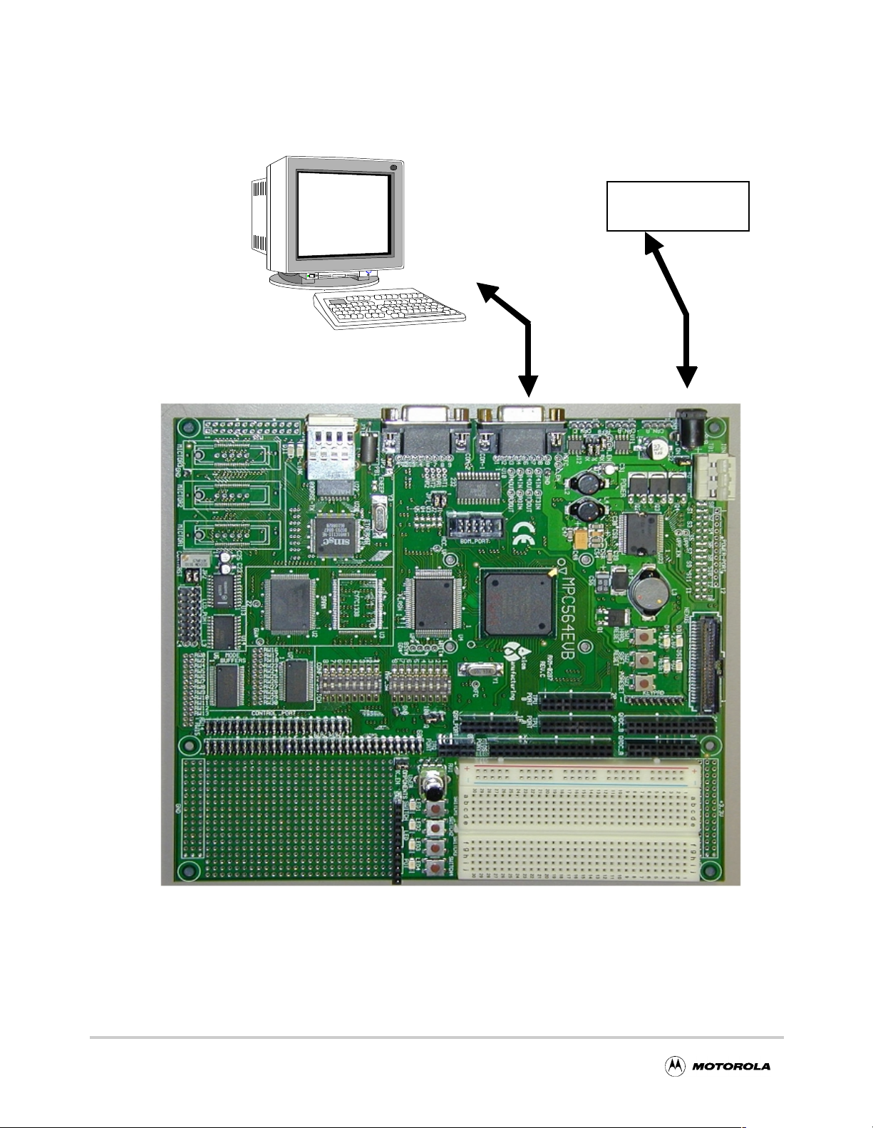
System Configuration
Freescale Semiconductor, Inc.
dBUG>
RS-232 Terminal
Or PC
nc...
I
cale Semiconductor,
6 - 26 V
Input Power
Frees
Figure 2-1. Minimum System Configuration
2-2 MPC564EVB User’s Manual
For More Information On This Product,
Go to: www.freescale.com
Page 41

nc...
I
cale Semiconductor,
Frees
Freescale Semiconductor, Inc.
Installation And Setup
2.2 Installation And Setup
The following sections describe all the steps needed to prepare the board for operation. Please read
the following sections carefully before using the board. When you are preparing the board for the
first time, be sure to check that all jumpers and switches are in the default locations. Default
jumper and switch settings are documented on the master jumper table (see Table 1-2). After the
board is functional in its default mode, the Ethernet interface may be used by following the
instructions provided in Appendix B, “Configuring dBUG for Network Downloads.
2.2.1 Unpacking
Unpack the computer board from its shipping box. Save the box for storing or reshipping. Refer
to the following list and verify that all the items are present. You should have received:
• MPC564EVB Single Board Computer
• MPC564EVB User's Manual (this document)
• One RS232 9-pin Serial Cable
• One CAT5E Ethernet cable, crossover type
• One P&E Micro BDM (Background Debug Mode) “wiggler” cable
• MPC5xx support CD with all documents, drawings, source codes, examples, AxIDE
software, and GNU compiler.
• 25-pin parallel cable (DB32 M/F) for BDM
• A selection of demo Third Party Developer Tools and Literature
NOTE:
Avoid touching the MOS devices. Static discharge can and will
damage these devices.
Once you have verified that all the items are present, remove the board from its protective jacket
and anti-static bag. Check the board for any visible damage. Ensure that there are no broken,
damaged, or missing parts. If you have not received all the items listed above or they are damaged,
please contact Axiom manufacturing immediately - for contact details please see the front of this
manual.
2.2.2 Preparing the Board for Use
The board, as shipped, is ready to be connected to a terminal and power supply without any need
for modification. Figure 2-3, “Jumper Locations”, shows the position of the jumpers and
connectors.
2.2.3 Providing Power to the Board
The board accepts two means of power supply connection, either PWR or TB1. Connector PWR
is a 2.1mm power jack and TB1 is a power clamp connector with inputs of +12VDC, Ground, and
an IGN (ignition) signal. If not using the provided power supply, the board accepts a supply voltage of 4 - 26VDC (current 300ma typical at 12VDC input).
Chapter 2. Initialization and Setup 2-3
For More Information On This Product,
Go to: www.freescale.com
Page 42

Freescale Semiconductor, Inc.
Installation And Setup
The Motorola MPC500 Family companion power supply Power Oak (PC33394) is provided on
the EVB board. This device provides many features designed for automotive applications but
may also be useful for industrial or general purpose applications. See the PC33394 data sheet for
full description of features, operation, and capability.
The Power Oak provides a regulated switch mode power source for the 2.6V, 3.3V, and 5V supplies on the EVB board. The basic application of the Power Oak provides the Reset signals,
back-up supplies for the KAPWR and IRAMSTBY to the MPC564, and the CAN A port transceiver. Many options are available on the board and some under software control via the MPC564
QSPI port to modify the Power Oak application.
The Power Port provides tap points for the power supplies and switched power outputs from the
Power Oak. Following is the Power Port pin assignment:
Table 2-1. Power Port Connections
PIN SIGNAL
nc...
I
1
+VIN DC supply
cale Semiconductor,
Frees
2 +5V
3 +3.3V
4 +2.6V
5 KAPWR
6IRAMSTBY
7 VDDSYN
8VREF1
9VREF2
10 VREF3
11 VPRE
12 VSEN
Refer to Power Oak document for application of the provided power sources.
TB1, ON Option, and PWR
TB1 Provides main input power source access and the Power Oak VIGN input signal. The +VIN
and ground sources may be applied or tapped from the TB1 pin 2 and 3 connections respectfully.
TB1 pin 1 provides access the VIGN signal to the Power Oak, user should note ON jumper operation in the following text.
The ON jumper provides a constant enable to the VIGN signal so the Power Oak is enabled upon
power application. The ON option jumper may be removed to apply the VIGN signal externally
with a switch or other source. Basic operation of the VIGN signal is to apply +VIN to enable the
2-4 MPC564EVB User’s Manual
For More Information On This Product,
Go to: www.freescale.com
Page 43

Freescale Semiconductor, Inc.
Power Oak supplies.
PWR jack connection provides power input from the supplied wall plug power source. Typical
input is +12VDC. The PWR jack provides a center positive terminal and ground outside sleeve.
The jack accepts 2.1mm inside x 5.5mm outside power plugs.
Installation And Setup
nc...
I
cale Semiconductor,
Frees
TB1 Front View
GND +VIN VIGN
PWR Front View
2mm Center Pin, Positive Volt
5.5mm Outer Ring, Ground
2.2.4 Select ing Terminal Baud Rate
The serial channel SCI0 of the MPC564 is used for serial communication and has a built in baud
rate generator. A number of baud rates can be programmed. On power-up or manual RESET, the
dBUG ROM monitor firmware configures the channel for 19200 baud. Once the dBUG ROM
monitor is running, a SET command may be issued to select any baud rate supported by the ROM
monitor. Refer to Chapter 3 for the discussion of this command.
2.2.5 The Terminal Character Format
The character format of the communication channel is fixed at power-up or RESET. The default
character format is 8 bits per character, no parity and one stop bit with no flow control. It is
neccessary to ensure that the terminal or PC is set to this format.
2.2.6 Connecting the Terminal
The board is now ready to be connected to a PC/terminal. Use the RS232 serial cable to connect
the PC/terminal to the MPC564EVB at COM-1. The cable has a 9-pin female D-sub terminal
connector at one end and a 9-pin male D-sub connector at the other end. Connect the 9-pin male
connector to connector COM-1 on the MPC564EVB board. Connect the 9-pin female connector
to one of the available serial communication channels normally referred to as COM1 (COM2, etc.)
on the PC running terminal emulation software (such as AxIDE, TeraTerm or Hyperterminal). The
connector on the PC/terminal may be either male 25-pin or 9-pin. It may be neccessary to obtain
a 25-pin-to-9-pin adapter to make this connection. If an adapter is required, refer to Figure 2-2
which shows the pin assignment for the 9-pin connector on the board.
2.2.7 Using a Personal Computer as a Terminal
A personal computer may be used as a terminal provided a terminal emulation software package is
available. Examples of this software are AxIDE, TeraTerm, PROCOMM, KERMIT, QMODEM,
Windows 95/98/2000 HyperTerminal or similar packages. The board should then be connected as
Chapter 2. Initialization and Setup 2-5
For More Information On This Product,
Go to: www.freescale.com
Page 44

Freescale Semiconductor, Inc.
MPC564EVB Jumper and Switch Setup
described in Section 2.2.6, “Connecting the Terminal.”
Once the connection to the PC is made, power may be applied to the PC and the terminal emulation
software can be run. In terminal mode, it is neccessary to select the baud rate and character format
for the channel. The character format should be 8 bits, no parity, one stop bit. (see Section 2.2.5,
“The Terminal Character Format”.) The baud rate should be set to 19200 and XON/XOFF flow
control should be turn on. Power can now be applied to the board.
5
1
69
Figure 2-2. Pin assignment for female (Terminal) connector.
Pin assignments are as follows.
nc...
I
Pin 1, 4, and 6 = group connected for DTR/DSR flow control null back to host
Pin 2 = TXD output (RS232 level)
Pin 3 = RXD input (RS232 level)
Pin 5 = Ground/Vss/Common
Pin 7 and 8 = group connected for RTS/CTS flow control null back to host
Pin 9 = open
2.3 MPC564EVB Jumper and Switch Setup
Jumper settings are as follows:
Note ‘*’ is used to indicate that default setting.
‘**’ is used to indicate mandatory setting for proper operation.
cale Semiconductor,
Table 2-2. Jumper Settings
Jumper Setting Function
Frees
JP1 * 1-2,3-4 COM2: TX=Pin3, RX=Pin2 (see silk screen on bottom of
board)
1-3,2-4 COM2: TX=Pin2, RX=Pin3 (see silk screen on bottom of
board)
JP2 Determines the display power pin polarity on the
LCD_PORT. See the schematic
JP3 *1-2 (closest to
RS232
connectors)
2-3 BDM being used runs at 2.6 volts.
BRK_EN *inserted SWITCH1 will act as a debounced Non-Maskable Interrupt
2-6 MPC564EVB User’s Manual
For More Information On This Product,
BDM being used runs at 3.3 vo lts. So the signals need to go
through a level shifter to get 2.6 volts to the part.
(ABORT)
Go to: www.freescale.com
Page 45

Freescale Semiconductor, Inc.
MPC564EVB Jumper and Switch Setup
Table 2-2. Jumper Settings (Continued)
Jumper Setting Function
removed SWITCH1 is for user use
B_RX *insterted CAN: see Section 1.4.2, “CAN PORTs and Options
removed CAN: see Section 1.4.2, “CAN PORTs and Options
C_TX inserted CAN: see Section 1.4.2, “CAN PORTs and Options
*removed CAN: see Section 1.4.2, “CAN PORTs and Options
C_RX inserted CAN: see Section 1.4.2, “CAN PORTs and Options
*removed CAN: see Section 1.4.2, “CAN PORTs and Options
100_IRQ *inserted
Ties the interrupt line from the Ethernet chip to
the interrupt line of the processor
removed Disconnects the interrupt line from the ethernet chip to the
nc...
I
“ON” * insterted Allows the board to have power.
removed Power to the board should b e controll ed by an ignition sw itch
interrupt line of the processor
connected to the IGN input on the Power Clamp, TB1.
Figure 2-3 on the next page shows the jumper locations for the board.
cale Semiconductor,
Frees
Chapter 2. Initialization and Setup 2-7
For More Information On This Product,
Go to: www.freescale.com
Page 46

Freescale Semiconductor, Inc.
MPC564EVB Jumper and Switch Setup
ON
J12
nc...
I
cale Semiconductor,
Frees
JP3
JP1
100_IRQ
BRK_EN
JP2
Figure 2-3. Jumper Locations on the Board
2.3.1 Reset Configuration Word and Configuration Switch (CONFIG_SW)
Configuration Switch provides several key external Reset Configuration W ord (RCW)options and
the programming enable options for programming the MPC564 internal flash memory. These
switches provide a logic 0 or low level when off and a logic 1 or high level when on. The RCW
2-8 MPC564EVB User’s Manual
For More Information On This Product,
Go to: www.freescale.com
Page 47

Freescale Semiconductor, Inc.
MPC564EVB Jumper and Switch Setup
configuration options are only presented to the data bus during Hard Reset if enabled by CONFIG
switch position 1. Note that MAP switch also has positions (5 and 8) that are part of the Reset
Configuration Word. All other RCW options can be located on the RW test pads, see RW options
for description of how to apply . The Reset Configuration Word options are all defaulted to logic 0
when the CONFIG Switches are in the OFF position. For more information on the MPC564 Reset
Configuration W ord refe r to the Reset Chapter in the MPC564 users manual. Five bits are available
on CONFIG_SW (see Table 2-3).I
Table 2-3. CONFIG_SW
nc...
I
cale Semiconductor,
Frees
Switch Name MPC563/564
Function
1CFG_ENRST_CONF
2CFG1 BDIS
3 CFG2 ETRE
4 CFG3 EN_COMP
5 CFG4 EXC_COMP
6CFG5 DME
7 EPEE EPEE
8 B0EPEE B0EPEE
Function
Enable External Config: This bit
enables the external reset config
Data Bus 3/Boot Dis: This bit enables booting from ex tern al flas h
memory
This switch controls the Except ion
Table Relocation feature
This switch enables Com pression
Mode
This switch controls whether Ex-
ception vector code is com-
pressed
This switch enables Dual Map-
ping
This pin enables erasing and programming of the internal MPC566
flash
This switch enables pro gramming
or erasing of BLock 0 th e intern al
flash
0 = Internal Reset Config Word se-
lected
1 = External Reset Config Word se-
lected (default)
0 = Boot from internal memory (de-
fault)
1 = Boot from external flash
0 = Exception table relocation is off
(default)
1 = Exception table relocation is on
0 = “Decompression ON” mode is dis-
abled (default)
1 = “Decompression ON” mode is en-
abled
0 = MPC564 assumes that the excep-
tion routines are non-compressed
(default)
1 = MPC564 assumes that all excep-
tion routines are compressed
0 = Dual Mapping disabled (default)
1 = Dual Mapping enabled
0 = Internal Flash P/E disabled
1 = Internal Flash P/E enabled (de-
fault)
0 =P/E of Block 0 disabled
1 = P/E of Block 0 enabled (default)
Notes:
1) Position 1 should be ON at all times until the MPC564 internal flash RCW word is pro-
grammed. This switch will cause the external value RCW to override the internal flash value of
the RCW word.
2) Position 7 and 8 must be enabled for MPC564 internal flash erase or programming operations.
3) All other external RCW bits are provided with the RW hardware options.
RW0 – 30: External Reset Configuration Word (RCW) Options
Chapter 2. Initialization and Setup 2-9
For More Information On This Product,
Go to: www.freescale.com
Page 48

Freescale Semiconductor, Inc.
System Power-up and Initial Operation
R W0, RW2, RW4 – 18, RW23 – 30 provide the user access to external Reset Configuration Word
(RCW) bits not normally required for default MPC564EVB operation. The RW0 – 30 designations
reflect the data bus D0 – D30 bit affected when the RCW word is enabled externally. All RW0 –
30 option bits are defaulted to the logic low value during external RCW word operation. The user
may apply a wire jumper between the 2 pad positions of each RW0 – 30 option to provide a logic
high level on the respective bit position during external RCW operation. Note that the user could
add physical headers (2mm type) to these signals on the board. Refer to the MPC564 user manual
Reset chapter for the respective RCW bit definitions.
2.3.2 Memory Configuration (MAP_SW)
The Memory Configuration switch (MAP_SW) controls the mapping of the MPC564 chip selects
to the different external memories and whether the internal flash is enabled.I
Table 2-4. MAP_SW
nc...
I
cale Semiconductor,
Frees
Switch Name MPC563/564
Function
1
2
3
4
5 IP RCW-IP IP bit is set on
6
7CS3-TA TA
8 2.6v FLEN Enable Internal MPC563/564 Flash off
1
Each Chip Select should only be connected to one device.
CS0
CS1
CS0
CS2
CS3
1
1
1
1
1
RAM_CS CS0 connected to the External SRAM off
RAM_CS CS1 connected to the External SRAM on
FL_CS CS0 connected to the External Flash on
FL_CS CS1 connected to the External Flash off
100_CS/LCD_
CS
CS3 connected to the Ethernet and LCD Interface on
TA for LCD or Connect the Et herNe t Controll er TA to t he Pro-
Switch Closed Default
cessor TA
2.4 System Power-up and Initial Operation
on
When all of the cables are connected to the board, power may be applied. The dBUG ROM Monitor
initializes the board and then displays a power-up message on the terminal.
Part Number: 0xXX
MaskNum: 0xXX
Copyright 1995-2002 Motorola, Inc. All Rights Reserved.
MPC564 MPC564EVB Firmware v3b.1a.xx (Build XXX on XXX XX 20XX
xx:xx:xx)
Enter ’help’ for help.
2-10 MPC564EVB User’s Manual
For More Information On This Product,
Go to: www.freescale.com
Page 49

Freescale Semiconductor, Inc.
dBUG>
The board is now ready for operation under the control of the debugger as described in Chapter 3.
If you do not get the above response, perform the following checks:
1. Make sure that the power supply is properly configured for polarity, voltage level and
current capability (~300mA) and is connected to the board.
2. Check that the terminal and board are set for the same character format and baud.
3. Check that your switches are set to their default settings.
4. Press the RESET button to insure that the board has been initialized properly.
If you still are not receiving the proper response, your board may have been damaged. Contact
Axiom Manufacturing for further instructions, please see the beginning of this manual for contact
details.
nc...
I
System Power-up and Initial Operation
cale Semiconductor,
Frees
Chapter 2. Initialization and Setup 2-11
For More Information On This Product,
Go to: www.freescale.com
Page 50

Freescale Semiconductor, Inc.
System Power-up and Initial Operation
nc...
I
cale Semiconductor,
Frees
2-12 MPC564EVB User’s Manual
For More Information On This Product,
Go to: www.freescale.com
Page 51

Freescale Semiconductor, Inc.
D:\TECD-SPO\Documentation\MPC564EVB\mpc564evb_3_Firmware_V1.fm 4/1/03
Chapter 3
Using the Monitor/Debug Firmware
The MPC564EVB single board computer has a resident firmware package that provides a
self-contained programming and operating environment. The firmware, named dBUG, provides
the user with monitor/debug interface, inline assembler and disassembly, program download,
register and memory manipulation, and I/O control functions. This chapter is a how-to-use
description of the dBUG package, including the user interface and command structure.
nc...
I
3.1 What Is dBUG?
cale Semiconductor,
Frees
dBUG is a traditional ROM monitor/debugger that offers a comfortable and intuitive command
line interface that can be used to download and execute code. It contains all the primary features
needed in a debugger to create a useful debugging environment.
The firmware (stored in the upper 1MByte of the Flash ROM device) provides a self-contained
programming and operating environment. dBUG interacts with the user through pre-defined
commands that are entered via the terminal. These commands are defined in Section 3.4,
“Commands”.
The user interface to dBUG is the command line. A number of features have been implemented to
achieve an easy and intuitive command line interface.
dBUG assumes that an 80x24 character dumb-terminal is utilized to connect to the debugger. For
serial communications, dBUG requires eight data bits, no parity, and one stop bit, 8N1 with no flow
control. The default baud rate is 19200 but can be changed after the power-up.
The command line prompt is “dBUG> “. Any dB UG command may be entered from this prompt.
dBUG does not allow command lines to exceed 80 characters. Wherever possible, dBUG displays
data in 80 columns or less. dBUG echoes each character as it is typed, eliminating the need for any
“local echo” on the terminal side.
In general, dBUG is not case sensitive. Commands may be entered either in upper or lower case,
depending upon the user’s equipment and preference. Only symbol names require that the exact
case be used.
Chapter 3. Using the Monitor/Debug Firmware 3-1
For More Information On This Product,
Go to: www.freescale.com
Page 52

Freescale Semiconductor, Inc.
Operational Procedure
Most commands can be recognized by using an abbreviated name. For instance, entering “h” is
the same as entering “help”. Thus, it is not necessary to type the entire command name.
The commands DI, GO, MD, STEP and TRACE are used repeatedly when debugging. dBUG
recognizes this and allows for repeated execution of these commands with minimal typing. After
a command is entered, simply press <RETURN> or <ENTER> to invoke the command again. The
command is executed as if no command line parameters were provided.
An additional function called the "System Call" allows the user program to utilize various routines
within dBUG. The System Call is discussed at the end of this chapter.
The operational mode of dBUG is demonstrated in Figure 3-1. After the system initialization, the
board waits for a command-line input from the user terminal. When a proper command is entered,
the operation continues in one of the two basic modes. If the command causes execution of the
user program, the dBUG firmware may or may not be re-entered, at the discretion of the user’s
program. For the alternate case, the command will be executed under control of the dBUG
firmware, and after command completion, the system returns to command entry mode.
nc...
I
cale Semiconductor,
Frees
During command execution, additional user input may be required depending on the command
function.
For commands that accept an optional <wi dth> to modify the memory access size, the va lid values
are:
• B 8-bit (byte) access
• H 16-bit (half-word) access
• W 32-bit (word) access
When no <width> option is provided, the default width is .W, 32-bit.
The core MPC500 register set is maintained by dBUG. These are listed below:
• GPR0-GPR31
• IP (SRR0 is IP)
• MSR (SRR1 is MSR)
• CR, XER, LR, CTR, DSISR, DAR, DEC
All control registers on MPC500 core are not readable by the supervisor-programming model, and
thus not accessible via dBUG. User code may change these registers, but caution must be exercised
as changes may render dBUG inoperable.
A reference to “SP” (stack pointer) actually refers to general purpose address register one, “GPR1."
3.2 Operational Procedure
System power-up and initial operation are described in detail in Chapter 2. This information is
repeated here for convenience and to prevent possible damage.
3.2.1 System Power-up
• Be sure the power supply is connected properly prior to power-up.
• Make sure the terminal is connected to RS232 COM-1 connector.
3-2 MPC564EVB User’s Manual
For More Information On This Product,
Go to: www.freescale.com
Page 53

Freescale Semiconductor, Inc.
• Make sure the IP bit is set (switch 5 ON in MAP_SW). This will cause the board to boot
out of external flash (where the dBUG code resides).
• Turn power on to the board.
nc...
I
Operational Procedure
cale Semiconductor,
Frees
Chapter 3. Using the Monitor/Debug Firmware 3-3
For More Information On This Product,
Go to: www.freescale.com
Page 54

Freescale Semiconductor, Inc.
Operational Procedure
Figure 3-1 shows the dUBG operational mode.
nc...
I
cale Semiconductor,
Frees
Figure 3-1. Flow Diagram of dBUG Operational Mode.
3.2.2 System Initialization
The act of powering up the board will initialize the system. The processor is reset and dBUG is
invoked.
dBUG performs the following configurations of internal resources during the initialization. The IP
bit is set by default, placing the vector table at 0xFFF0_0000 (external SRAM). To take over an
3-4 MPC564EVB User’s Manual
For More Information On This Product,
Go to: www.freescale.com
Page 55

Freescale Semiconductor, Inc.
exception vector, the user places the address of the exception handler in the appropriate vector in
the vector table located at 0xFFF0_0000.
The Software Watchdog Timer is disabled and internal timers are placed in a stop condition.
Interrupt controller registers are initialized with unique interrupt level/priority pairs. Please refer
to the dBUG source files on the PowerPC website (www.motorola.com/powerpc) for the complete
initialization code sequence.
After initialization, the terminal will display:
Part Number: 0x36
MaskNum: 0x10
Copyright 1995-2002 Motorola, Inc. All Rights Reserved.
MPC564
Enter ’help’ for help.
MPC564EVB Firmware v2e.1a.xx (Build XXX on XXX XX 20XX xx:xx:xx)
Operational Procedure
nc...
I
cale Semiconductor,
Frees
dBUG>
If you did not get this response check the setup, refer to Section 2.4, “System Power-up and Initia l
Operation”.
Other means can be used to re-initialize the MPC564EVB Computer Board firmware. These
means are discussed in the following paragraphs.
3.2.2.1 Hard RESET Button.
Pressing the Hard RESET button (SW1-HARD RESET) causes all processes to terminate, resets
the MPC564 processor and board logic and restarts the dBUG firmware. Pressing the RESET
button would be the appropriate action if all else fails.
3.2.2.2 Non-Maskable Interrupt Button.
SWITCH1 can be used as a non-maskable interrupt button. It is available for the user to use in their
code as an input if the jumper BRK_EN is removed. The NMI function causes an interrupt of the
present processing (a level 0 interrupt on MPC564) and gives control to the dBUG firmware. This
action differs from RESET in that no processor register or memory contents are changed, the
processor and peripherals are not reset, and dBUG is not restarted. Also, in response to depressing
the NMI button, the contents of the MPC564 core internal registers are displayed.
The NMI function is most appropriate when software is being debugged. The user can interrupt
the processor without destroying the present state of the system. This is accomplished by forcing
a non-maskable interrupt that will call a dBUG routine that will save the current state of the
registers to shadow registers in the monitor for display to the user . The user will be returned to the
ROM monitor prompt after exception handling.
3.2.2.3 Software Reset Command.
dBUG does have a command that causes dBUG to restart as if a hardware reset was invoked. The
command is "RESET".
Chapter 3. Using the Monitor/Debug Firmware 3-5
For More Information On This Product,
Go to: www.freescale.com
Page 56

Command Line Usage
Freescale Semiconductor, Inc.
3.3 Command Line Usage
The user interface to dBUG is the command line. A number of features have been implemented to
achieve an easy and intuitive command line interface.
dBUG assumes that an 80x24 ASCII character dumb terminal is used to connect to the debugger.
For serial communications, dBUG requires eight data bits, no parity, and one stop bit (8N1). The
baud rate default is 19200 bps — a speed commonly available from workstations, personal
computers and dedicated terminals.
The command line prompt is: dBUG>
Any dBUG command may be entered from this prompt. dBUG does not allow command lines to
exceed 80 characters. Wherever possible, dBUG displays data in 80 columns or less. dBUG echoes
each character as it is typed, eliminating the need for any local echo on the terminal side.
The <Backspace> and <Delete> keys are recognized as rub-out keys for correcting typographical
mistakes.
nc...
I
Command lines may be recalled using the <Control> U, <Control> D and <Control> R key
sequences. <Control> U and <Control> D cycle up and down through previous command lines.
<Control> R recalls and executes the last command line.
cale Semiconductor,
Frees
In general, dBUG is not case-sensitive. Commands may be entered either in uppercase or
lowercase, depending upon the user’s equipment and preference. Only symbol names require that
the exact case be used.
Most commands can be recognized by using an abbreviated name. For instance, entering h is the
same as entering help. Thus it is not necessary to type the entire command name.
The commands DI, GO, MD, STEP and TRACE are used repeatedly when debugging. dBUG
recognizes this and allows for repeated execution of these commands with minimal typing. After
a command is entered, press the <Return> or <Enter> key to invoke the command again. The
command is executed as if no command line parameters were provided.
3.4 Commands
This section lists the commands that are available with all versions of dBUG. Some boa rd or C PU
combinations may use additional commands not listed below.
Table 3-1. dBUG Command Summary
MNEMONIC
ASM asm <<addr> stmt> Assemble
BC bc addr1 addr2 length Block Compare
BF bf <width> begin end data <inc> Block Fill
BM bm begin end dest Block Move
BR br addr <-r> <-c count> <-t trigger> Breakpoint
BS bs <width> begin end data Block Search
DC dc value Data Convert
DI di<addr> Disassemble
DL dl <offset> Download Serial
DLDBUG dldbug Download dBUG
DN dn <-c> <-e> <-i> <-s <-o offset>> <filename> Download Network
SYNTAX
DESCRIPTION
3-6 MPC564EVB User’s Manual
For More Information On This Product,
Go to: www.freescale.com
Page 57

Freescale Semiconductor, Inc.
Commands
Table 3-1. dBUG Command Summary
MNEMONIC
FL fl <command> dest <src> size Erase/Program External
GO go <addr> Execute
GT gt addr Execute To
HBR hbr addr <-r> Hardware Breakpoint
HELP help <command> Help
IRD ird <module.register> Internal Register Display
IRM irm module.register data Internal Register Modify
LR lr<width> addr Loop Read
LW lw<width> addr data Loop Write
MD md<width> <begin> <end> Memory Disp lay
MM mm<width> addr <data> Memory Modify
MMAP mmap Memory Ma p Dis pl ay
RD rd <reg> Register Display
nc...
I
RM rm reg data Register Modify
RESET reset Reset
SD sd Stack Dump
SET set <option value> Set Configurations
SHOW show <option> Show Configurations
STEP step Step (Over)
SYMBOL symbol <symb> <-a symb value> <-r sy mb> <-C|l |s>Symbol Management
TRACE trace <num> Trace (Into)
VERSION version Show Version
SYNTAX
cale Semiconductor,
DESCRIPTION
Flash
Frees
Chapter 3. Using the Monitor/Debug Firmware 3-7
For More Information On This Product,
Go to: www.freescale.com
Page 58

Commands
Freescale Semiconductor, Inc.
ASM Assembler
Usage: ASM <<addr> stmt>
The ASM command is a primitive assembler. The <stmt> is assembled and the resulting code
placed at <addr>. This command has an interactive and non-interactive mode of operation.
The value for address <addr> may be an absolute address specified as a hexadecimal value, or a
symbol name. The value for stmt must be valid assembler mnemonics for the CPU.
For the interactive mode, the user enters the command and the optional <addr>. If the address is
not specified, then the last addre ss is used. The me mory c onten ts at the address a re disasse mbled,
and the user prompted for the new assembly. If valid, the new assembly is placed into memory , and
the address incremented accordingly. If the assembly is not valid, then memory is not modified,
and an error message produced. In either case, memory is disassembled and the process repeats.
The user may press the <Enter> or <Return> key to accept the current memory contents and skip
to the next instruction, or a enter period to quit the interactive mode.
nc...
I
cale Semiconductor,
Frees
In the non-interactive mode, the user specifies the address and the assembly statement on the
command line. The statement is the assembled, and if valid, placed into memory , otherwise an error
message is produced.
Examples:
To place a NOP instruction at address 0x0001_0000, the command is:
asm 10000 nop
To interactively assembly memory at address 0x0040_0000, the command is:
asm 400000
3-8 MPC564EVB User’s Manual
For More Information On This Product,
Go to: www.freescale.com
Page 59

Freescale Semiconductor, Inc.
Commands
BC Block Compare
Usage: BC addr1 addr2 length
The BC command compares two contiguous blocks of memory on a byte by byte basis. The first
block starts at address addr1 and the second starts at address addr2, both of length bytes.
If the blocks are not identical, the address of the first mismatch is displayed. The value for
addresses addr1 and addr2 may be an absolute address specified as a hexadecimal value or a
symbol name. The value for length may be a symbol name or a number converted according to the
user defined radix (hexadecimal by default).
Example:
T o verify that the data starting at 0xFFF2_0000 and ending at 0xFFF3_0000 is identical to the data
starting at 0xFFF0_0000, the command is:
bc FFF20000 FFF00000 10000
nc...
I
cale Semiconductor,
Frees
Chapter 3. Using the Monitor/Debug Firmware 3-9
For More Information On This Product,
Go to: www.freescale.com
Page 60

Commands
Freescale Semiconductor, Inc.
BF Block Fill
Usage: BF<width> begin end data <inc>
The BF command fills a contiguous block of memory starting at address begin, stopping at address
end, with the value data. <Width> modifies the size of the data that is written. If no <width> is
specified, the default of word sized data is used.
The value for addresses begin and end may be an absolute address specified as a hexadecimal
value, or a symbol name. The value for data may be a symbol name, or a number converted
according to the user-defined radix, normally hexadecimal.
The optional value <inc> can be used to increment (or decrement) the data value during the fill.
This command first aligns the starting address for the data access size, and then increments the
address accordingly during the operation. Thus, for the duration of the operation, this command
performs properly-aligned memory accesses.
Examples:
nc...
I
To fill a memory block starting at 0xFFF2_0000 and ending at 0xFFF4_0000 with the value
0x1234, the command is:
cale Semiconductor,
Frees
bf FFF20000 FFF40000 1234
To fill a block of memory starting at 0xFFF20000 and ending at 0xFFF4_0000 with a byte value
of 0xAB, the command is:
bf.b FFF20000 FFF40000 AB
T o zero out t he BSS section of the t arget code (defined by the symbols bss_start and bss_end), the
command is:
bf bss_start bss_end 0
To fill a block of memory starting at 0xFFF2_0000 and ending at 0xFFF4_0000 with data that
increments by 2 for each <width>, the command is:
bf FFF20000 FFF40000 0 2
3-10 MPC564EVB User’s Manual
For More Information On This Product,
Go to: www.freescale.com
Page 61

Freescale Semiconductor, Inc.
Commands
BM Block Move
Usage: BM begin end dest
The BM command moves a contiguous block of memory starting at address begin and stopping at
address end to the new address dest. The BM command copies memory as a series of bytes, and
does not alter the original block.
The values for addresses begin, end, and dest may be absolute addresses specified as hexadecimal
values, or symbol names. If the destination address overlaps the block defined by begin and end,
an error message is produced and the command exits.
Examples:
To copy a block of memory starting at 0xFFF4_0000 and ending at 0xFFF7_0000 to the location
0xFFF0_0000, the command is:
bm FFF40000 FFF70000 FFF00000
nc...
I
cale Semiconductor,
Frees
To copy the target code’s data section (defined by the symbols data_start and data_end) to
0xFFF0_0000, the command is:
bm data_start data_end FFF00000
NOTE:
Refer to “upuser” command for copying code/data into Flash
memory.
Chapter 3. Using the Monitor/Debug Firmware 3-11
For More Information On This Product,
Go to: www.freescale.com
Page 62

Commands
Freescale Semiconductor, Inc.
BR Breakpoints
Usage: BR addr <-r> <-c count> <-t trigger>
The BR command inserts or removes software breakpoints at address addr. The value for addr may
be an absolute address specified as a hexadecimal value, or a symbol name. Count and trigger are
numbers converted according to the user-defined radix, normally hexadecimal.
If no argument is provided to the BR command, a listing of all defined breakpoints is displayed.
The -r option to the BR command removes a breakpoint defined at address addr. If no address is
specified in conjunction with the -r option, then all breakpoints are removed.
Each time a breakpoint is encountered during the execution of target code, its count value is
incremented by one. By default, the initial count value for a breakpoint is zero, but the -c option
allows setting the initial count for the breakpoint.
Each time a breakpoint is encountered during the execution of target code, the count value is
compared against the trigger value. If the count value is equal to or greater than the trigger value,
nc...
I
a breakpoint is encountered and control returned to dBUG. By default, the initial trigger value for
a breakpoint is one, but the -t option allows setting the initial trigger for the breakpoint.
cale Semiconductor,
Frees
If no address is specified in conjunction with the -c or -t options, then all breakpoints a re initialized
to the values specified by the -c or -t option.
Examples:
To set a breakpoint at the C function main() (symbol _main; see “symbol” command), the
command is:
br _main
When the target code is executed and the processor reaches main(), control will be returned to
dBUG.
To set a breakpoint at the C function bench() and set its trigger value to 3, the command is:
br _bench -t 3
When the target code is executed, the processor must attempt to execute the function bench() a third
time before returning control back to dBUG.
To remove all breakpoints, the command is:
br -r
3-12 MPC564EVB User’s Manual
For More Information On This Product,
Go to: www.freescale.com
Page 63

Freescale Semiconductor, Inc.
Commands
BS Block Search
Usage: BS<width> begin end data
The BS command searches a contiguous block of memory starting at address begin, stopping at
address end, for the value data. <Width> modifies the size of the data that is compared during the
search. If no <width> is specified, the default of word sized data is used.
The values for addresses begin and end may be absolute addresses specified as hexadecimal values,
or symbol names. The value for data may be a symbol name or a number converted according to
the user-defined radix, normally hexadecimal.
This command first aligns the starting address for the data access size, and then increments the
address accordingly during the operation. Thus, for the duration of the operation, this command
performs properly-aligned memory accesses.
Examples:
To search for the 32-bit value 0x1234_5678 in the memory block starting at 0xFFF4_0000 and
nc...
I
ending at 0xFFF7_0000:
bs FFF40000 FFF70000 12345678
cale Semiconductor,
Frees
This reads the 32-bit word located at 0x0004_0000 and compares it against the 32-bit value
0x1234_5678. If no match is found, then the address is incremented to 0x0004_0002 and the next
32-bit value is read and compared.
T o search for the 16-bit value 0x1234 in the memory block starting at 0xFFF4_0000 and ending at
0xFFF7_0000:
bs 40000 FFF70000 1234
This reads the 32-bit word located at 0xFFF4_0000 and compares it against the 16-bit value
0x0000_1234. If no match is found, then the address is incremented to 0xFFF4_0004 and the next
32-bit value is read and compared.
Chapter 3. Using the Monitor/Debug Firmware 3-13
For More Information On This Product,
Go to: www.freescale.com
Page 64

Commands
Freescale Semiconductor, Inc.
DC Data Conversion
Usage: DC data
The DC command displays the hexadecimal or decimal value data in hexadecimal, binary, and
decimal notation.
The value for data may be a symbol na me or an absolute value. If an absolute value pass ed into the
DC command is prefixed by ‘0x’, then data is interpreted as a hexadecimal value. Otherwise data
is interpreted as a decimal value.
All values are treated as 32-bit quantities.
Examples:
To display the decimal and binary equivalent of 0x1234, the command is:
dc 0x1234
To display the hexadecimal and binary equivalent of 1234, the command is:
nc...
I
dc 1234
cale Semiconductor,
Frees
3-14 MPC564EVB User’s Manual
For More Information On This Product,
Go to: www.freescale.com
Page 65

Freescale Semiconductor, Inc.
Commands
DI Disassemble
Usage: DI <addr>
The DI command disassembles target code pointed to by addr. The value for addr may be an
absolute address specified as a hexadecimal value, or a symbol name.
Wherever possible, the disassembler will use information from the symbol table to produce a more
meaningful disassembly . This is especially useful for branch target addresses and subroutine calls.
The DI command attempts to track the address of the last disassembled opcode. If no address is
provided to the DI command, then the DI command uses the address of the last opcode that was
disassembled.
The DI command is repeatable.
Examples:
To disassemble code that starts at 0xFFF4_0000, the command is:
nc...
I
To disassemble code of the C function main(), the command is:
di FFF40000
cale Semiconductor,
Frees
di _main
Chapter 3. Using the Monitor/Debug Firmware 3-15
For More Information On This Product,
Go to: www.freescale.com
Page 66

Commands
Freescale Semiconductor, Inc.
DL Download Console
Usage: DL <offset>
The DL command performs an S-record download of data obtained from the console typically
through a serial port. The value for offset is converted according to the user-defined radix, normally
hexadecimal.
If offset is provided, then the destination address of each S-record is adjusted by offset.
The DL command checks the destination download address for validity. If the destination is an
address outside the defined user space, then an error message is displayed and downloading
aborted. DL can be used for downloading to internal flash, external flash, internal SRAM, and
external SRAM.
If the S-record file contains the entry point address, then the program counter is set to reflect this
address.
Examples:
nc...
I
To download an S-record file through the serial port, the command is:
cale Semiconductor,
Frees
dl
To download an S-record file through the serial port, and add an offset to the destination address
of 0x40, the command is:
dl 0x40
3-16 MPC564EVB User’s Manual
For More Information On This Product,
Go to: www.freescale.com
Page 67

Freescale Semiconductor, Inc.
Commands
DLDBUG Download dBUG
Usage: D LDBUG
The DLDBUG command will download the dBUG monitor to the MPC564EVB board. First it will erase
all sectors of Fl ash that dBUG occupies , then it will downl oad the c ode throug h the ser ial port . Upon aski ng
if the user is sure th ey want to do t his, the use r should r espond by typi ng “yes” if they want to continue. The
DLDBUG command will work at baud rates up to and including 57600.
Xon/Xoff flow control needs to be turned on in the terminal window to download data.
To download the dBUG monitor to the board, the command is:
dldbug
nc...
I
cale Semiconductor,
Frees
Chapter 3. Using the Monitor/Debug Firmware 3-17
For More Information On This Product,
Go to: www.freescale.com
Page 68

Commands
Freescale Semiconductor, Inc.
DN Download Network
Usage: DN <-c> <-e> <-i> <-s> <-o offset> <filename>
The DN command downloads code from the network. The DN command handle files which are
either S-record, COFF, ELF or Image formats. The DN command uses Trivial File Transfer
Protocol (TFTP) to transfer files from a network host.
In general, the type of file to be downloaded and the name of the file must be specified to the DN
command. The -c option indicates a COFF download, the -e option indicates an ELF download,
the -i option indicates an Image download, and the -s indicates an S-record download. The -o
option works only in conjunction with the -s option to indicate an optional offset for S-record
download. The filename is passed directly to the TFTP server and therefore must be a valid
filename on the server.
If neither of the -c, -e, -i, -s or filename options are specified, then a default filename and filetype
will be used. Default filename and filetype parameters are manipulated using the SET and SHOW
commands.
nc...
I
The DN command checks the destination download address for validity. If the destination is an
address outside the defined user space, then an error message is displayed and downloading
aborted.
cale Semiconductor,
Frees
For ELF and COFF files which contain symbolic debug information, the symbol tables are
extracted from the file during download and used by dBUG. Only global symbols are kept in
dBUG . The dBUG symbo l table is not cleared prior to downloading, so it is the user’s responsibility
to clear the symbol table as necessary prior to downloading.
If an entry point address is specified in the S-record, COFF or ELF file, the program counter is set
accordingly.
Examples:
To download an S-record file with the name “srec.out”, the command is:
dn -s srec.out
To download a COFF file with the name “coff.out”, the command is:
dn -c coff .out
To download a file using the default filetype with the name “bench.out”, the command is:
dn bench.out
To download a file using the default filename and filetype, the command is:
dn
3-18 MPC564EVB User’s Manual
For More Information On This Product,
Go to: www.freescale.com
Page 69

Freescale Semiconductor, Inc.
Commands
FL Erase/Program Flash
Usage: FL
FL (e)rase addr bytes
FL (w)rite dest src bytes
The FL command is used to erase the external flash, write to external flash, and display flash device
information. Erase and Write operations must be done in sector blocks. dBUG assumes that the user has
erased enough memory before writing to it. The destination address must be word (4byte) aligned and the
byte count must be in word (4byte) multiples. To download a .s19 file straight to flash, please see the DL
command.
nc...
I
cale Semiconductor,
Frees
Examples:
To view the flash device information, the command is:
fl
To erase 0x10000 bytes of flash starting at 0x00800000, the command is:
fl erase 800000 10000
T o copy 0x40 bytes of data from internal SRAM (0x3FA000) to external flash at 0x00800000, the command
is:
fl write 800000 3fa000 0x40
Chapter 3. Using the Monitor/Debug Firmware 3-19
For More Information On This Product,
Go to: www.freescale.com
Page 70

Commands
Freescale Semiconductor, Inc.
GO Execute
Usage: GO <addr>
The GO command executes target code starting at address addr. The value for addr may be an
absolute address specified as a hexadecimal value, or a symbol name.
If no argument is provided, the GO command begins executing instructions at the current program
counter.
When the GO command is executed, all user-defined breakpoints are inserted into the target code,
and the context is switched to the target program. Control is only regained when the target code
encounters a breakpoint, illegal instruction, or other exception which causes control to be handed
back to dBUG.
The GO command is repeatable.
Examples:
nc...
I
cale Semiconductor,
Frees
To execute code at the current program counter, the command is:
go
To execute code at the C function main(), the command is:
go _main
To execute code at the address 0x0004_0000, the command is:
go 40000
3-20 MPC564EVB User’s Manual
For More Information On This Product,
Go to: www.freescale.com
Page 71

Freescale Semiconductor, Inc.
Commands
GT Execute To
Usage: GT addr
The GT command inserts a temporary software breakpoint at addr and then executes target code
starting at the current program counter. The value for addr may be an absolute address specified as
a hexadecimal value, or a symbol name.
When the GT command is executed, all breakpoints are inserted into the target code, and the
context is switched to the target program. Control is only regained when the tar get code encounters
a breakpoint, illegal instruction, or other exception which causes control to be handed back to
dBUG.
Examples:
To execute code up to the C function bench(), the command is:
gt _bench
nc...
I
cale Semiconductor,
Frees
Chapter 3. Using the Monitor/Debug Firmware 3-21
For More Information On This Product,
Go to: www.freescale.com
Page 72

Commands
Freescale Semiconductor, Inc.
HELP Help
Usage: HELP <command>
The HELP command displays a brief syntax of the commands available within dBUG. In addition,
the address of where user code may start is given. If command is provided, then a brief listing of
the syntax of the specified command is displayed.
Examples:
To obtain a listing of all the commands available within dBUG, the command is:
help
To obtain help on the breakpoint command, the command is:
help br
nc...
I
cale Semiconductor,
Frees
3-22 MPC564EVB User’s Manual
For More Information On This Product,
Go to: www.freescale.com
Page 73

Freescale Semiconductor, Inc.
Commands
IRD Internal Register Display
Usage: IRD <module.register>
This command displays the internal registers of different modules inside the MPC500. In the
command line, module refers to the module name where the register is located and register refers
to the specific register to display.
The registers are organized according to the module to which they belong. The available mo dules
on the MPC500 are USIU, TPU_A, TPU_B, QADC_A, QADC_B, QSMCM_A, MIOS14,
CAN_A. Refer to the MPC564 user’s manual for more information on these modules and the
registers they contain.
Example:
ird usiu.plprcrk
nc...
I
cale Semiconductor,
Frees
Chapter 3. Using the Monitor/Debug Firmware 3-23
For More Information On This Product,
Go to: www.freescale.com
Page 74

Commands
Freescale Semiconductor, Inc.
IRM Internal Register Modify
Usage: IRM module.register data
This command modifies the contents of the internal registers of different modules inside the
MPC500. In the command line, module refers to the module name where the register is located and
register refers to the specific register to modify. The data parameter specifies the new value to be
written into the register.
The registers are organized according to the module to which they belong. The available mo dules
on the MPC500 are USIU, TPU_A, TPU_B, QADC_A, QADC_B, QSMCM_A, MIOS14,
CAN_A. Refer to the MPC564 user’s manual for more information on these modules and the
registers they contain.
Example:
To modify the PCPRCR in the USIU to the value 0x0091_4000, the command is:
irm usiu.plprcr 914000
nc...
I
cale Semiconductor,
Frees
3-24 MPC564EVB User’s Manual
For More Information On This Product,
Go to: www.freescale.com
Page 75

Freescale Semiconductor, Inc.
Commands
LR Loop Read
Usage: LR<width> addr
The LR command continually reads the data at addr until a key is pressed. The optional <width>
specifies the size of the data to be read. If no <width> is specified, the command defaults to reading
word sized data.
Example:
To continually read the word data from address 0xFFF2_0000, the command is:
lr FFF20000
nc...
I
cale Semiconductor,
Frees
Chapter 3. Using the Monitor/Debug Firmware 3-25
For More Information On This Product,
Go to: www.freescale.com
Page 76

Commands
Freescale Semiconductor, Inc.
LW Loop Write
Usage: LW<width> addr data
The LW command continually writes data to addr. The optional width specifies the size of the
access to memory. The default access size is a word.
Examples:
To continually write the data 0x1234_5678 to address 0xFFF2_0000, the command is:
lw FFF20000 12345678
Note that the following command writes 0x78 into memory:
lw.b FFF20000 12345678
nc...
I
cale Semiconductor,
Frees
3-26 MPC564EVB User’s Manual
For More Information On This Product,
Go to: www.freescale.com
Page 77

Freescale Semiconductor, Inc.
Commands
MD Memory Display
Usage: MD<width> <begin> <end>
The MD command displays a contiguous block of memory starting at address begin and stopping
at address end. The values for addresses begin and end may be absolute addresses specified as
hexadecimal values, or symbol names. Width modifies the size of the data that is displayed. If no
<width> is specified, the default of word sized data is used.
Memory display starts at the address begin. If no beginning address is provided, the MD command
uses the last address that was displayed. If no ending address is provided, then MD will display
memory up to an address that is 128 beyond the starting address.
This command first aligns the starting address for the data access size, and then increments the
address accordingly during the operation. Thus, for the duration of the operation, this command
performs properly-aligned memory accesses.
Examples:
nc...
I
cale Semiconductor,
Frees
To display memory at address 0x0040_0000, the command is:
md 400000
To display memory in the data section (defined by the symbols data_start and data_end), the
command is:
md data_start
To display a range of bytes from 0x00040000 to 0x0005_0000, the command is:
md.b 40000 50000
To display a range of 32-bit values starting at 0x0004_0000 and ending at 0x0005_0000:
md 40000 50000
Chapter 3. Using the Monitor/Debug Firmware 3-27
For More Information On This Product,
Go to: www.freescale.com
Page 78

Commands
Freescale Semiconductor, Inc.
MM Memory Modify
Usage: MM<width> addr <data>
The MM command modifies memory at the address addr. The value for addr may be an absolute
address specified as a hexadecimal value, or a symbol name. Width specifies the size of the data
that is modified. If no <width> is specified, the default of word sized data is used. The value for
data may be a symbol name, or a number converted according to the user-defined radix, normally
hexadecimal.
If a value for data is provided, then the MM command imm ediately sets the contents of addr to data .
If no value for data is provided, then the MM command enters into a loop. The loop obtains a value
for data, sets the contents of the current address to data, increments the address according to the
data size, and repeats. The loop terminates when an invalid entry for the data value is entered, i.e.,
a period.
This command first aligns the starting address for the data access size, and then increments the
address accordingly during the operation. Thus, for the duration of the operation, this command
nc...
I
performs properly-aligned memory accesses.
Examples:
cale Semiconductor,
Frees
To set the byte at location 0xFFF1_0000 to be 0xFF, the command is:
mm.b FFF10000 FF
To interactively modify memory beginning at 0xFFF1_0000, the command is:
mm FFF10000
3-28 MPC564EVB User’s Manual
For More Information On This Product,
Go to: www.freescale.com
Page 79

Freescale Semiconductor, Inc.
Commands
MMAP Memory Map Display
Usage: mmap
This command displays the memory map information for the MPC564 evaluation board. The
information displayed includes the type of memory, the start and end address of the memory, and
the port size of the memory . The display also includes information on how the Chip-selects are used
on the board.
Here is an example of the output from this command:
Type Start End
---------------------------------------ISB 0x00000000 0x003FFFFF
Internal SRAM 0x003F8000 0x003FFFFF
Flash 0x00800000 0x009FFFFF
nc...
I
User Flash 0x00800000 0x008FFFFF
dBUG Flash 0x00900000 0x009FFFFF
Ethernet 0x01000000 0x01008000
External SRAM 0xFFF00000 0xFFF7FFFF
User Space 0xFFF08000 0xFFF7FFFF
cale Semiconductor,
Frees
Chapter 3. Using the Monitor/Debug Firmware 3-29
For More Information On This Product,
Go to: www.freescale.com
Page 80

Commands
Freescale Semiconductor, Inc.
RD Register Display
Usage: RD <reg>
The RD command displays the register set of the target. If no argument for reg is provided, then all
registers are displayed. Otherwise, the value for reg is displayed.
dBUG preserves the registers by storing a copy of the register set in a buffer. The RD command
displays register values from the register buffer.
Examples:
To display all the registers and their values, the command is:
rd
To display only the program counter:
rd pc
nc...
I
cale Semiconductor,
Frees
Here is an example of the output from this command:
pc: FFF08000 msr: 00009042 [EE,ME,IP,RI]
cr: 00000000 xer: 00000000 lr: 00000000 ctr: 00000000
r00-07: 00000000 003FFF00 00000000 00000000 00000000 00000000 00000000 00000000
r08-15: 00000000 00000000 00000000 00000000 00000000 00000000 00000000 00000000
r16-23: 00000000 00000000 00000000 00000000 00000000 00000000 00000000 00000000
r24-31: 00000000 00000000 00000000 00000000 00000000 00000000 00000000 00000000
3-30 MPC564EVB User’s Manual
For More Information On This Product,
Go to: www.freescale.com
Page 81

Freescale Semiconductor, Inc.
Commands
RM Register Modify
Usage: RM reg data
The RM command modifies the contents of the register reg to data. The value for reg is the name
of the register, and the value for data may be a symbol name, or it is converted according to the
user-defined radix, normally hexadecimal.
dBUG preserves the registers by storing a copy of the register set in a buffer. The RM command
updates the copy of the register in the buffer. The actual value will not be written to the register
until target code is executed.
Examples:
To change program counter to contain the value 0x003f_8000, the command is:
rm pc 3f8000
nc...
I
cale Semiconductor,
Frees
Chapter 3. Using the Monitor/Debug Firmware 3-31
For More Information On This Product,
Go to: www.freescale.com
Page 82

Commands
Freescale Semiconductor, Inc.
RESET Reset the Board and dBUG
Usage: RESET
The RESET command resets dBUG to it’s initial power-on states.
The RESET command executes the same sequence of code that occurs at power-on. If the RESET
command fails to reset the system adequately, cycle the power or press the reset button.
Examples:
To reset the board and clear the dBUG data structures, the command is:
reset
nc...
I
cale Semiconductor,
Frees
3-32 MPC564EVB User’s Manual
For More Information On This Product,
Go to: www.freescale.com
Page 83

nc...
I
cale Semiconductor,
Frees
Freescale Semiconductor, Inc.
Commands
SET Set Configurations
Usage: SET <option value>
The SET command allows the setting of user-configurable options within dBUG. With no
arguments, SET displays the options and values available. The SHOW command displays the
settings in the appropriate format. The standard set of options is listed below.
• baud - This is the baud rate for the first serial port on the board. All communications
between dBUG and the user occur using either 9600 or 19200 bps, eight data bits, no parity,
and one stop bit, 8N1, with no flow control.
• speed - This is the clock speed of the processor. Changing the speed parameter will
automatically configure the part’s wait states as well as the wait cycles on the external flash.
The default is 56MHz. The only clock speeds supported in dBUG are 40, 56, and 66 MHz
(not every MPC564EVB supports 66MHz. Make sure you have a MPC564CZP66
processor before switching to this speed).
• base - This is the default radix for use in converting a number from its ASCII text
representation to the internal quantity used by dBUG . The default is hexadecimal (base 16),
and other choices are binary (base 2), octal (base 8), and decimal (base 10).
• client - This is the network Internet Protocol (IP) address of the board. For network
communications, the client IP is required to be set to a unique value, usually assigned by
your local network administrator.
• server - This is the network IP address of the machine which contains files accessible via
TFTP. Your local network administrator will have this information and can assist in
properly configuring a TFTP server if one does not exist.
• gateway - This is the network IP address of the gateway for your local subnetwork. If the
client IP address and server IP address are not on the same subnetwork, then this option
must be properly set. Your local network administrator will have this information.
• netmask - This is the network address mask to determine if use of a gateway is required.
This field must be properly set. Your local network administrator will have this
information.
• filename - This is the default filename to be used for network download if no name is
provided to the DN command.
• filetype - This is the default file type to be used for network download if no type is provided
to the DN command. Valid values are: “srecord”, “coff”, and “elf”.
• ethaddr - This is the ethernet address (a.k.a hardware address) for the evaluation board. This
should be set to a unique value, and the most significant nibble should always be even.
Examples:
To set the baud rate of the board to be 19200, the command is:
set baud 19200
To set the clock speed of the processor to be 40MHz, the command is:
set speed 40
NOTE:
See the SHOW command for a display containing the correct formatting of these
options.
Chapter 3. Using the Monitor/Debug Firmware 3-33
For More Information On This Product,
Go to: www.freescale.com
Page 84

Commands
Freescale Semiconductor, Inc.
SHOW Show Configurations
Usage: SHOW <option>
The SHOW command displays the settings of the user-configurable options within dBUG. When
no option is provided, SHOW displays all options and values.
Examples:
To display all options and settings, the command is:
show
To display the current baud rate of the board, the command is:
show baud
Here is an example of the output from a show command:
dBUG> show
nc...
I
cale Semiconductor,
Frees
base: 16
baud: 19200
server: 192.0.0.1
client: 192.0.0.2
gateway: 0.0.0.0
netmask: 255.255.255.0
filename: test.srec
filetype: S-Record
mac: 00:CF:52:49:C3:01
speed: 56000000
3-34 MPC564EVB User’s Manual
For More Information On This Product,
Go to: www.freescale.com
Page 85

Freescale Semiconductor, Inc.
Commands
STEP Step Over
Usage: STEP
The STEP command can be used to “step over” a subroutine call, rather than tracing every
instruction in the subroutine. The ST command sets a temporary software breakpoint one
instruction beyond the current program counter and then executes the target code. This command
only works when executing code in SRAM.
The STEP command can be used to “step over” BSR and JSR instructions.
The STEP command will work for other instructions as well, but note that if the STEP command
is used with an instruction that will not return, i.e. BRA, then the temporary breakpoint may never
be encountered and dBUG may never regain control.
Examples:
To pass over a subroutine call, the command is:
nc...
I
cale Semiconductor,
Frees
step
Chapter 3. Using the Monitor/Debug Firmware 3-35
For More Information On This Product,
Go to: www.freescale.com
Page 86

Commands
Freescale Semiconductor, Inc.
SYMBOL Symbol Name Management
Usage: SYMBOL <symb> <-a symb value> <-r symb> <-c|l|s>
The SYMBOL command adds or removes symbol names from the symbol table. If only a symbol
name is provided to the SYMBOL command, then the symbol table is searched for a match on the
symbol name and its information displayed.
The -a option adds a symbol name and its value into the symbol table. The -r option removes a
symbol name from the table.
The -c option clears the entire symbol table, the -l option lists the contents of the symbol table, and
the -s option displays usage information for the symbol table.
Symbol names contained in the symbol table are truncated to 31 characters. Any symbol table
lookups, either by the SYMBOL command or by the disassembler, will only use the first 31
characters. Symbol names are case-sensitive.
Symbols can also be added to the symbol table via in-line assembly labels and ethernet downloads
nc...
I
of ELF formatted files.
Examples:
cale Semiconductor,
Frees
To define the symbol “main” to have the value 0xFFF4_0000, the command is:
symbol -a main FFF40000
To remove the symbol “junk” from the table, the command is:
symbol -r junk
To see how full the symbol table is, the command is:
symbol -s
To display the symbol table, the command is:
symbol -l
3-36 MPC564EVB User’s Manual
For More Information On This Product,
Go to: www.freescale.com
Page 87

Freescale Semiconductor, Inc.
Commands
TRACE Trace Into
Usage: TRACE <num>
The TRACE command allows single-instruction execution. If num is provided, then num
instructions are executed before control is handed back to dBUG. The value for num is a decimal
number.
The TRACE command sets bits in the processors’ supervisor registers to achieve single-instruction
execution, and the target code executed. Control returns to dBUG after a single-instruction
execution of the target code.
This command is repeatable.
Examples:
To trace one instruction at the program counter, the command is:
tr
nc...
I
cale Semiconductor,
Frees
To trace 20 instructions from the program counter, the command is:
tr 20
Chapter 3. Using the Monitor/Debug Firmware 3-37
For More Information On This Product,
Go to: www.freescale.com
Page 88

Commands
Freescale Semiconductor, Inc.
VERSION Display dBUG Version
Usage: VERSION
The VERSION command displays the version information for dBUG. The dBUG version, build
number and build date are all given.
The version number is separated by a decimal, for example, “v 2b.1c.1a”.
In this example, v 3b . 1a . 1a
dBUG common
major and minor
revision
nc...
I
The version date is the day and time at which the entire dBUG monitor was compiled and built.
Examples:
To display the version of the dBUG monitor, the command is:
version
CPU major
and minor
revision
cale Semiconductor,
{
{
{
board major
and minor
revision
Frees
3-38 MPC564EVB User’s Manual
For More Information On This Product,
Go to: www.freescale.com
Page 89

Freescale Semiconductor, Inc.
System Call Functions
3.5 System Call Functions
An additional utility within the dBUG firmware is a function ca lled the Syste m Call handler. This
function can be called by the user program to utilize various routines within dBUG, to perform a
special task, and to return control to dBUG. This section describes the System Call handler and
how it is used.
There are 6 System Call functions. These are: OUT_CHAR, IN_CHAR, IN_STAT,
ISR_REGISTER, ISR_REMOVE and EXIT_TO_dBUG. The system call interface accepts an
opcode in r10 to indicate which operation is to be performed. Various results are returned, usually
in r3. When these routines are invoked, the following is true: sprg0 contains r31 and sprg1 contains
LR.
3.5.1 OUT_CHAR
This function (function code 0x0020) sends a character, which is in r3, to terminal. The system call
nc...
I
interface accepts an opcode in r10 to indicate which operation is to be performed.
Assembly example:
cale Semiconductor,
Frees
/* assume r3 contains the character */
addi r10, r0, 0x0020 Selects the function
sc The character in r3 is sent to terminal
C example:
/* assume r3 contains the character */
void board_out_char (int ch)
{
asm(“ addi r10, r0, 0x0020”); Selects the function
asm(“ sc”); The character in r3 is sent to terminal
}
3.5.2 IN_CHAR
This function (function code 0x0000) returns an input character (from terminal) to the caller. The
returned character is in r3.
Assembly example:
/* the character is returned to the user in r3*/
addi r10, r0, 0x0000 Selects the function
sc The character is returned in r3
C example:
int board_in_char (void)
Chapter 3. Using the Monitor/Debug Firmware 3-39
For More Information On This Product,
Go to: www.freescale.com
Page 90

System Call Functions
{ /* assume r3 contains the character */
asm(“ addi r10, r0, 0x0000”); Selects the function
asm(“ sc”); The character is returned in r3
}
Freescale Semiconductor, Inc.
3.5.3 IN_STAT
This function (function code 0x0001) checks if an input character is present to receive. A value of
zero is returned in r3 when no character is present. A value of 1 in r3 means a character is present.
Assembly example:
addi r10, r0, 0x0001 Select the function
sc Make the call, r3 contains the response (yes/no).
C example:
nc...
I
cale Semiconductor,
Frees
int board_char_present (void)
{
asm( "addi r10,r0,0x0001");Select the function
asm( "sc"); Make the call, r3 contains the response (yes/no).
}
3.5.4 ISR_REGISTER
This function’s code is 0x0040. For ISR_REGISTER, the vector, handler, device ptr, and arg ptr
are in r3, r4, r5, and r6 respectively.
C example:
int
board_isr_register (int vector, void *handler, void *device, void *arg)
{
/*
* Vector will normally be 0x0500 for IRQ. Handler should be address
* of your routine. Device and Arg are both used as arguments to
* Handler when it is invoked. Ie. handler(device,arg); It is
* intended that Device point to the device. If the handler is
* registered OK, 1 is returned, otherwise 0.
*/
asm( "addi r10,r0,0x0040");
asm( "sc");
}
3.5.5 ISR_REMOVE
This function’s code is 0x0041. For ISR_REMOVE, the vector is in r3. Nothing is returned.
Assembly example:
addi r10, r0, 0x0041 Selects the function
sc The character is returned in r3
3-40 MPC564EVB User’s Manual
For More Information On This Product,
Go to: www.freescale.com
Page 91

C example:
Freescale Semiconductor, Inc.
int
board_isr_remove (void *handler)
{
asm( "addi r10,r0,0x0041");
asm( "sc");
}
System Call Functions
3.5.6 EXIT_TO_dBUG
This function transfers the control back to the dBUG, by terminating the user code. The register
context is preserved.
nc...
I
C example (see “scif.s”file : anything in R10 besides 0x0000, 0x0001, 0x0020, 0x0030, 0x0031,
0x0040, 0x0041):
cale Semiconductor,
Frees
asm( "addi r10,r0,0x0063");
asm( "sc");
Chapter 3. Using the Monitor/Debug Firmware 3-41
For More Information On This Product,
Go to: www.freescale.com
Page 92

Freescale Semiconductor, Inc.
System Call Functions
nc...
I
cale Semiconductor,
Frees
3-42 MPC564EVB User’s Manual
For More Information On This Product,
Go to: www.freescale.com
Page 93

Freescale Semiconductor, Inc.
Appendix A
MPC533/534 Emulation
The MPC564EVB can be used to emulate the MPC533 and MPC534 processors. This appendix
will highlight the differences between the processors. Several modules present in the MPC564 are
not available in the MPC533/4, so the user should not reference those modules.
Table A-1 compares the MPC564, MPC533, and MPC534 module lists. Figure A-1shows the
block diagram of the MPC533/4.
nc...
I
cale Semiconductor,
Frees
.
T able A-1. Module Differences of MPC564, MPC533, and
MPC534
Module MPC564 MPC533 MPC534
Core Speed 40 or 56 or
66MHz
Termperature
Range
Code
Compression
FLASH 512K 512K 512K
Static RAM 32K 32K 32K
TPU3 (2) N/A N/A
DPTRAM 8K N/A N/A
QADC Module (2) (1) QADC_A (1) QADC_A
TouCAN (CAN
Versi on 2.0 B )
-40oC to +85oC
and
o
C to +125oC
-40
available N/A available
(3) CAN_A,
CAN_B, CAN_C
40MHz 40MHz
o
C to +85oC-40oC to +85oC
-40
(1) CAN_B (1) CAN_B
Appendix A. MPC533/534 Emulation A-1
For More Information On This Product,
Go to: www.freescale.com
Page 94
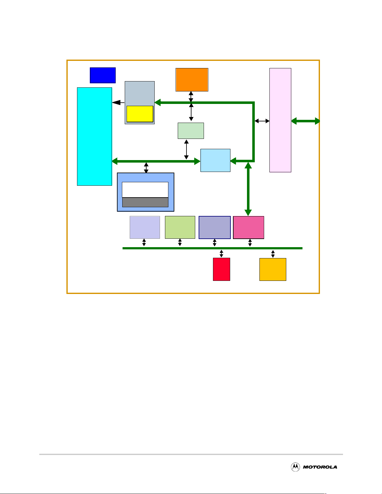
Block Diagram
Freescale Semiconductor, Inc.
Figure A-1. Block Diagram of the MPC533/4
JTAG
Burst
Buffer
Controller 2
DECRAM
(2Kbytes)
MPC500
Core
+
FPU
nc...
I
32K CALRAM
28 Kbytes
4-Kbyte Overlay
QADC64E
L-BUS
cale Semiconductor,
512 Kbytes
Nexus
QSMCM
Flash*
Tou
CAN
L2U
PPM
CAN
U-BUS
Tou
UIMB
Tou
CAN
USIU
MIOS14
IMB3
E-BUS
Frees
A-2 MPC564EVB User’s Manual
For More Information On This Product,
Go to: www.freescale.com
Page 95

Freescale Semiconductor, Inc.
Appendix B
Configuring dBUG for Network
Downloads
The dBUG module has the ability to perform downloads over an Ethernet network using the T rivial
File Transfer Protocol, TFTP (NOTE: this requires a TFTP server to be running on the host
attached to the board). Prior to using this feature, several parameters are required for network
nc...
I
downloads to occur. The information that is required and the steps for configuring dBUG are
described below.
cale Semiconductor,
Frees
B.1 Required Network Parameters
For performing network downloads, dBUG needs 6 parameters; 4 are network-related, and 2 are
download-related. The parameters are listed below, with the dBUG designation following in
parenthesis.
All computers connected to an Ethernet network running the IP protocol need 3 network-specific
parameters. These parameters are:
Internet Protocol, IP, address for the computer (client IP),
IP address of the Gateway for non-local traffic (gateway IP), and
Network netmask for flagging traffic as local or non-local (netmask).
In addition, the dBUG network download command requires the following three parameters:
IP address of the TFTP server (server IP),
Name of the file to download (filename),
Type of the file to download (filetype of S-record, COFF, ELF, or Image).
Your local system administrator can assign a unique IP address for the board, and also provide you
the IP addresses of the gateway, netmask, and TFTP server. Fill out the lines below with this
information.
Client IP:___.___.___.___(IP address of the board)
Server IP:___.___.___.___(IP address of the TFTP server)
Gateway:___.___.___.___(IP address of the gateway)
Netmask:___.___.___.___(Network netmask)
B.2 Configuring dBUG Network Parameters
Once the network parameters have been obtained, the dBUG Rom Monitor must be configured.
The following commands are used to configure the network parameters.
set client <client IP>
set server <server IP>
MPC564EVB User’s Manual B-1
For More Information On This Product,
Go to: www.freescale.com
Page 96

Freescale Semiconductor, Inc.
Troubleshooting Network Problems
set gateway <gateway IP>
set netmask <netmask>
set ethaddr <addr>
For example, the TFTP se rver is named ‘santafe’ and has IP addre ss 123.45.67.1. The board is
assigned the IP address of 123.45.68.15. The gateway IP address is 123.45.68.250, and the
netmask is 255.255.255.0. The ethaddr address is chosen arbitrarily and is unique. The commands
to dBUG are:
set client 123.45.68.15
set server 123.45.67.1
set gateway 123.45.68.250
set netmask 255.255.255.0
set ethaddr 00:CF:52:49:C3:01
The last step is to inform dBUG of the name and type of the file to download. Prior to giving the
name of the file, keep in mind the following.
nc...
I
cale Semiconductor,
Frees
Most, if not all, TFTP servers will only permit access to files starting at a particular sub-directory.
(This is a security feature which prevents reading of arbitrary files by unknown per sons.) For
example, SunOS uses the directory /tftp_boot as the default TFTP directory. When specifying a
filename to a SunOS TFTP server, all filenames are relative to /tftp_boot. As a result, you normally
will be required to copy the file to download into the directory used by the TFTP server.
A default filename for network downloads is maintained by dBUG. To change the default
filename, use the command:
set filename <filename>
When using the Ethernet network for download, either S-record, COFF, ELF, or Image files may
be downloaded. A default filetype for network downloads is maintained by dBUG as well. To
change the default filetype, use the command:
set filetype <srecord|coff|elf|image>
Continuing with the above example, the compiler produces an executable COFF file, ‘a.out’. This
file is copied to the /tftp_boot directory on the server with the command:
rcp a.out santafe:/tftp_boot/a.out
Change the default filename and filetype with the commands:
set filename a.out
set filetype coff
Finally, perform the network download with the ‘dn’ command. The network download process
uses the configured IP addresses and the default filename and filetype for initiating a TFTP
download from the TFTP server.
B.3 Troubleshooting Network Problem s
Most problems related to network downloads are a direct result of improper configuration. Verify
that all IP addresses configured into dBUG are correct. This is accomplished via the ‘show
’command.
Using an IP address already assigned to another machine will cause dBUG network download to
B-2 MPC564EVB User’s Manual
For More Information On This Product,
Go to: www.freescale.com
Page 97

Freescale Semiconductor, Inc.
fail, and probably other severe network problems. Make certain the client IP address is unique for
the board.
Check for proper insertion or connection of the network cable. Is the status LED lit indicating that
network traffic is present?
Check for proper configuration and operation of the TFTP server. Most Unix workstations can
execute a command named ‘tftp’ which can be used to connect to the TFTP server as well. Is the
default TFTP root directory present and readable?
If ‘ICMP_DESTINATION_UNREACHABLE’ or similar ICMP message appears, then a serious
error has occurred. Reset the board, and wait one minute for the TFTP server to time out and
terminate any open connections. V erify that the IP addresses for the server and gateway are correct.
Also verify that a TFTP server is running on the server.
nc...
I
Troubleshooting Network Problems
cale Semiconductor,
Frees
MPC564EVB User’s Manual B-3
For More Information On This Product,
Go to: www.freescale.com
Page 98

Freescale Semiconductor, Inc.
Troubleshooting Network Problems
nc...
I
cale Semiconductor,
Frees
B-4 MPC564EVB User’s Manual
For More Information On This Product,
Go to: www.freescale.com
 Loading...