

Page 1

查询MPC180LMB供应商
MPC180LMB Security Processor
User’s Manual
PRELIMINARY—SUBJECT TO CHANGE WITHOUT NOTICE
MPC180LMBUM/D
Rev. 0, 3/2002
Page 2

DigitalDNA, PowerQUICC, and PowerQUICC II are trademarks of Motorola, Inc.
The PowerPC name, the PowerPC logotype, and PowerPC 603e are trademarks of International Business Machines Corporation
used by Motorola under license from International Business Machines Corporation.
2
I
C is a registered trademark of Philips Semiconductors
This document contains information on a new product under development. Motorola reserves the right to change or discontinue this
product without notice. Information in this document is provided solely to enable system and software implementers to use Motorola
security processors. There are no express or implied copyright licenses granted hereunder to design or fabricate Motorola security
processors integrated circuits or integrated circuits based on the information in this document.
Motorola reserves the right to make changes without further notice to any products herein. Motorola makes no warranty,
representation or guarantee regarding the suitability of its products for any particular purpose, nor does Motorola assume any liability
arising out of the application or use of any product or circuit, and specifically disclaims any and all liability, including without limitation
consequential or incidental damages. “Typical” parameters can and do vary in different applications. All operating parameters,
including “Typicals” must be validated for each customer application by customer’s technical experts. Motorola does not convey any
license under its patent rights nor the rights of others. Motorola products are not designed, intended, or authorized for use as
components in systems intended for surgical implant into the body, or other applications intended to support or sustain life, or for any
other application in which the failure of the Motorola product could create a situation where personal injury or death may occur.
Should Buyer purchase or use Motorola products for any such unintended or unauthorized application, Buyer shall indemnify and
hold Motorola and its officers, employees, subsidiaries, affiliates, and distributors harmless against all claims, costs, damages, and
expenses, and reasonable attorney fees arising out of, directly or indirectly, any claim of personal injury or death associated with such
unintended or unauthorized use, even if such claim alleges that Motorola was negligent regarding the design or manufacture of the
part. Motorola and are registered trademarks of Motorola, Inc. Motorola, Inc. is an Equal Opportunity/Affirmative Action Employer.
Motorola Literature Distribution Centers:
USA/EUROPE: Motorola Literature Distribution; P.O. Box 5405; Denver, Colorado 80217; Tel.: 1-800-441-2447 or 1-303-675-2140/
JAPAN: Nippon Motorola Ltd SPD, Strategic Planning Office 4-32-1, Nishi-Gotanda Shinagawa-ku, Tokyo 141, Japan Tel.: 81-35487-8488
ASIA/PACIFC: Motorola Semiconductors H.K. Ltd.; 8B Tai Ping Industrial Park, 51 Ting Kok Road, Tai Po, N.T., Hong Kong;
Tel.: 852-26629298
Technical Information: Motorola Inc. SPS Customer Support Center 1-800-521-6274; electronic mail address:
crc@wmkmail.sps.mot.com.
Document Comments: FAX (512) 933-3873, Attn: Security Processor Applications Engineering.
World Wide Web Addresses: http://www.motorola.com/smartnetworks/products/security
http://www.mot.com/netcomm
http://www.mot.com/PowerPC
http://www.mot.com/HPESD
© Motorola Inc. 2002. All rights reserved.
Page 3

Overview
1
Signal Descriptions
External Bus Interface and Memory Map
Data Encryption Standard Execution Unit
Arc Four Execution Unit
Message Digest Execution Unit
Public Key Execution Unit
Random Number Generator
2
3
4
5
6
7
8
Glossary of Terms and Abbreviations
PRELIMINARY—SUBJECT TO CHANGE WITHOUT NOTICE
GLO
Page 4

1
Overview
2
3
4
5
6
7
8
Signal Descriptions
External Bus Interface and Memory Map
Data Encryption Standard Execution Unit
Arc Four Execution Unit
Message Digest Authentication Unit
Public Key Execution Unit
Random Number Generator
GLO
Glossary of Terms and Abbreviations
PRELIMINARY—SUBJECT TO CHANGE WITHOUT NOTICE
Page 5

v
CONTENTS
Paragraph
Number
Title
Page
Number
Chapter 1
Overview
1.1 Features............................................................................................................... 1-1
1.2 System Architecture............................................................................................ 1-2
1.3 Architectural Overview....................................................................................... 1-3
1.3.1 Public Key Execution Unit (PKEU)............................................................... 1-4
1.3.2 Data Encryption Standard Execution Unit (DEU).......................................... 1-4
1.3.3 Arc Four Execution Unit (AFEU) .................................................................. 1-5
1.3.4 Message Authentication Unit (MAU)............................................................. 1-5
1.3.5 Random Number Generator (RNG)................................................................ 1-5
1.3.6 Software and Hardware Support..................................................................... 1-6
Chapter 2
Signal Descriptions
2.1 Signal Descriptions............................................................................................. 2-1
Chapter 3
External Bus Interface and Memory Map
3.1 Execution Unit Registers .................................................................................... 3–1
3.2 Address Map....................................................................................................... 3–2
3.3 External Bus Interface......................................................................................... 3–4
3.3.1 EBI Registers.................................................................................................. 3–5
3.3.1.1 Command/Status Register (CSTAT).......................................................... 3–5
3.3.1.2 ID Register.................................................................................................. 3–7
3.3.1.3 IMASK Register......................................................................................... 3–8
3.3.1.4 Input Buffer Control (IBCTL) and Output Buffer Control (OBCTL) Registers
3–9
3.3.1.5 Input Buffer Count (IBCNT) and Output Buffer Count (OBCNT) Registers...
3–11
3.4 EBI Controller Operation.................................................................................. 3–11
3.4.1 Buffer Accesses (FIFO Mode)...................................................................... 3–11
Contents
Page 6

vi
CONTENTS
Paragraph
Number
Title
Page
Number
Chapter 4
Data Encryption Standard Execution Unit
4.1 Operational Registers.......................................................................................... 4–1
4.1.1 DEU Control Register (DCR)......................................................................... 4–2
4.1.2 DEU Configuration Register (DCFG)............................................................ 4–2
4.1.3 DEU Status Register (DSR)............................................................................ 4–3
4.1.4 Key Registers.................................................................................................. 4–4
4.1.5 Initialization Vector........................................................................................ 4–4
4.1.6 DATAIN......................................................................................................... 4–4
4.1.7 DATAOUT..................................................................................................... 4–4
Chapter 5
Arc Four Execution Unit
5.1 Arc Four Execution Unit Registers..................................................................... 5–1
5.1.1 Status Register ................................................................................................ 5–2
5.1.2 Control Register.............................................................................................. 5–3
5.1.3 Clear Interrupt Register .................................................................................. 5–3
5.1.4 Key Length Register....................................................................................... 5–3
5.1.5 Key (Low/Lower-middle/Upper-middle/Upper) Register.............................. 5–3
5.1.6 Message Byte Double-Word Register ............................................................ 5–4
5.1.7 Message Register............................................................................................ 5–4
5.1.8 Cipher Register............................................................................................... 5–4
5.1.9 S-box I/J Register............................................................................................ 5–5
5.1.10 S-box0 – S-box63 Memory............................................................................. 5–5
Chapter 6
Message Digest Execution Unit
6.1 Operational Registers.......................................................................................... 6–1
6.1.1 MDEU Version Identification Register (MID)............................................... 6–2
6.1.2 MDEU Control Register (MCR)..................................................................... 6–2
6.1.3 Status Register (MSR).................................................................................... 6–4
6.1.4 Message Buffer (MB0—MB15)..................................................................... 6–5
6.1.5 Message Digest Buffer (MA–ME) ................................................................. 6–5
Chapter 7
Public Key Execution Unit
7.1 Operational Registers.......................................................................................... 7–1
7.1.1 PKEU Version Identification Register (PKID) .............................................. 7–1
MPC180LMB Security Processor User’s Manual
Page 7

CONTENTS
Paragraph
Number
Title
Page
Number
7.1.2 Control Register (PKCR)................................................................................ 7–2
7.1.3 Status Register (PKSR)................................................................................... 7–3
7.1.4 Interrupt Mask Register (PKMR)................................................................... 7–4
7.1.5 EXP(k) Register.............................................................................................. 7–6
7.1.6 Program Counter Register (PC)...................................................................... 7–6
7.1.7 Modsize Register ............................................................................................ 7–7
7.1.8 EXP(k)_SIZE.................................................................................................. 7–7
7.2 Memories ............................................................................................................ 7–7
7.3 ECC Routines ..................................................................................................... 7–8
7.3.1 ECC Fp Point Multiply................................................................................... 7–8
7.3.2 ECC Fp Point Add........................................................................................ 7–11
7.3.3 ECC Fp Point Double................................................................................... 7–12
7.3.4 ECC Fp Modular Add................................................................................... 7–13
7.3.5 ECC Fp Modular Subtract ............................................................................ 7–14
7.3.6 ECC Fp Montgomery Modular Multiplication
B × R-1) mod N) 7–15
((A ×
7.3.7 ECC Fp Montgomery Modular Multiplication
B × R-2) mod N) 7–16
((A ×
m
7.3.8 ECC F2
7.3.9 ECC F2
7.3.10 ECC F2
7.3.11 ECC F2
7.3.12 ECC F2
((A ×
7.3.13 ECC F2
((A ×
Polynomial-Basis Point Multiply................................................. 7–17
m
Point Add...................................................................................... 7–19
m
Point Double................................................................................ 7–21
m
Add (Subtract)............................................................................. 7–22
m
Montgomery Modular Multiplication
B × R-1) mod N) 7–23
m
Montgomery Modular Multiplication
B × R-2) mod N) 7–24
7.4 RSA Routines ................................................................................................... 7–25
-1
EXP
R
)
7.4.1 (A ×
mod N .................................................................................... 7–25
7.4.2 RSA Montgomery Modular Multiplication
((A ×
B × R-1) mod N) 7–27
7.4.3 RSA Montgomery Modular Multiplication
((A ×
B × R-2) mod N) 7–28
7.4.4 RSA Modular Add........................................................................................ 7–29
7.4.5 RSA Fp Modular Subtract ............................................................................ 7–30
7.5 Miscellaneous Routines.................................................................................... 7–31
7.5.1 Clear Memory............................................................................................... 7–31
2
7.5.2 R
7.5.3 R
mod N Calculation................................................................................... 7–32
R
mod P Calculation .............................................................................. 7–33
p
N
7.6 Embedded Routine Performance ...................................................................... 7–35
Chapter 8
Random Number Generator
Contents
vii
Page 8

CONTENTS
Paragraph
Number
8.1 Overview............................................................................................................. 8–1
8.2 Functional Description........................................................................................ 8–1
8.3 Typical Operation ............................................................................................... 8–1
8.4 Random Number Generator Registers................................................................ 8–2
8.4.1 Status Register ................................................................................................ 8–2
Title
Page
Number
Glossary of Terms and Abbreviations
viii
MPC180LMB Security Processor User’s Manual
Page 9

ix
ILLUSTRATIONS
Figure
Number
Title
Page
Number
1-1 Typical MPC8xx System Example............................................................................... 1-2
1-2 Typical MPC8260 System Example............................................................................. 1-3
1-3 MPC180 Block Diagram...............................................................................................1-3
2-1 MPC180 Pin Diagram................................................................................................... 2-4
3-1 MPC180 Execution Unit Registers...............................................................................3–1
3-2 Command/Status Register (CSTAT) ............................................................................3–6
3-3 ID Register....................................................................................................................3–8
3-4 IMASK Register ...........................................................................................................3–9
3-5 Input Buffer Control (IBCTL) and Output Buffer Control (OBCTL) Registers........3–10
3-6 Input Buffer Count (IBCNT) and Output Buffer Count (OBCNT) Registers...........3–11
4-1 DES Control Register (DCR)........................................................................................4–2
4-2 DEU Configuration Register (DCFG)..........................................................................4–2
4-3 DES Status Register (DSR) ..........................................................................................4–3
5-1 Arc Four Execution Unit Status Register......................................................................5–2
5-2 Arc Four Execution Unit Control Register...................................................................5–3
5-3 Arc Four Execution Unit Message Byte Double-Word Register..................................5–4
6-1 MDEU Control Register (MCR)...................................................................................6–2
6-2 MDEU Status Register (MSR)......................................................................................6–4
7-1 PKEU Control Register (PKCR) ..................................................................................7–2
7-2 PKEU Status Register (PKSR) .....................................................................................7–4
7-3 PKEU Interrupt Mask Register (PKMR)......................................................................7–5
7-4 ECC Fp Point Multiply Register Usage........................................................................7–9
7-5 ECC Fp Point Add Register Usage.............................................................................7–11
7-6 ECC Fp Point Double Register Usage........................................................................7–12
7-7 Modular Add Register Usage......................................................................................7–13
7-8 Modular Subtract Register Usage...............................................................................7–14
7-9 Modular Multiplication Register Usage......................................................................7–15
7-10 Modular Multiplication (with double reduction) Register Usage...............................7–16
m
7-11 ECC F2
7-12 ECC F2
7-13 ECC F2
7-14 F2
7-15 F2
7-16 F2
m
m
m
Point Multiply I/O......................................................................................7–18
m
Point Add Register Usage ..........................................................................7–20
m
Point Double Register Usage .....................................................................7–21
Modular Add (Subtract) Register Usage.............................................................7–22
Modular Multiplication Register Usage..............................................................7–23
Modular Multiplication (with double reduction) Register Usage.......................7–24
7-17 Integer Modular Exponentiation Register Usage........................................................7–26
7-18 Modular Multiplication Register Usage......................................................................7–27
Contents
Page 10

ILLUSTRATIONS
x
Figure
Number
Title
Page
Number
7-19 Modular Multiplication (with double reduction) Register Usage...............................7–28
7-20 Modular Add Register Usage......................................................................................7–29
7-21 Modular Subtract Register Usage...............................................................................7–30
7-22 Clear Memory Register Usage....................................................................................7–31
2
7-23 R
7-24 R
mod N Register Usage...........................................................................................7–33
R
mod P Register Usage ......................................................................................7–34
P
N
8-1 RNG Status Register.....................................................................................................8–2
MPC180LMB Security Processor User’s Manual
Page 11

TABLES
Table
Number
Title
Page
Number
2-1 Pin Descriptions............................................................................................................ 2-1
3-1 32-Bit System Address Map.........................................................................................3–2
3-2 EBI Registers................................................................................................................3–5
3-3 CSTAT Field Descriptions ...........................................................................................3–6
3-4 ID Field Descriptions....................................................................................................3–8
3-5 IMASK Field Descriptions...........................................................................................3–9
3-6 IBCTL Field Descriptions...........................................................................................3–10
3-7 OBCTL Register Field Descriptions...........................................................................3–10
4-1 Data Encryption Standard Execution Unit (DEU) Registers........................................4–1
4-2 DCR Field Descriptions................................................................................................4–2
4-3 DCFG Field Descriptions .............................................................................................4–3
4-4 DSR Field Descriptions ................................................................................................4–3
5-1 Arc Four Execution Unit (AFEU) Registers.................................................................5–1
5-2 AFEU Status Register Field Descriptions.....................................................................5–2
5-3 AFEU Control Register Field Descriptions..................................................................5–3
6-1 Message Digest Execution Unit (MDEU) Registers ....................................................6–1
6-2 MCR Field Descriptions...............................................................................................6–3
6-3 MSR Field Descriptions................................................................................................6–4
7-1 PKEU Registers............................................................................................................7–1
7-2 PKCR Field Descriptions..............................................................................................7–2
7-3 PKSR Field Descriptions..............................................................................................7–4
7-4 PKMR Field Descriptions.............................................................................................7–5
7-5 ECC Fp Point Multiply.................................................................................................7–8
7-6 ECC Fp Point Add......................................................................................................7–11
7-7 ECC Fp Point Double .................................................................................................7–12
7-8 Modular Add...............................................................................................................7–13
7-9 Modular Subtract ........................................................................................................7–14
7-10 Modular Multiplication...............................................................................................7–15
7-11 Modular Multiplication (with double reduction)........................................................7–16
m
7-12 ECC F2
7-13 ECC F2
7-14 ECC F2
7-15 F2
7-16 F2
7-17 F2
m
m
m
Point Multiply.............................................................................................7–17
m
Point Add....................................................................................................7–20
m
Point Double...............................................................................................7–21
Modular Add (Subtract)......................................................................................7–22
Modular Multiplication.......................................................................................7–23
Modular Multiplication (with double reduction) ................................................7–24
7-18 Integer Modular Exponentiation.................................................................................7–26
Contents
xi
Page 12

TABLES
Table
Number
Title
Page
Number
7-19 Modular Multiplication...............................................................................................7–27
7-20 Modular Multiplication (with double reduction)........................................................7–28
7-21 Modular Add...............................................................................................................7–29
7-22 Modular Subtract ........................................................................................................7–30
7-23 Clear Memory.............................................................................................................7–31
2
7-24 R
7-25 R
mod N ....................................................................................................................7–32
R
mod P................................................................................................................7–34
p
N
7-26 Run Time Formulas ....................................................................................................7–35
8-1 Random Number Generator Registers..........................................................................8–2
8-2 RNG Status Register Field Descriptions.......................................................................8–2
xii
MPC180LMB Security Processor User’s Manual
Page 13

Chapter 1
Overview
This chapter gives an overview of the MPC180 security processor, including the key
features, typical system architecture, and the MPC180 internal architecture.
1.1 Features
The MPC180 is a flexible and powerful addition to an y netw orking system currently using
Motorola’s MPC8xx or MPC826x family of PowerQUICC™ communication processors.
The MPC180 is designed to off-load computationally intensive security functions such as
key generation and exchange, authentication, and bulk data encryption.
The MPC180 is optimized to process all of the algorithms associated with IPSec, IKE,
WTLS/WAP and SSL/TLS. In addition, the MPC180 is the only security processor on the
market capable of executing the elliptic curv e cryptography that is especially important for
secure wireless communications.
MPC180 features include the following:
• Public key execution unit (PKEU), which supports the following:
— RSA and Diffie-Hellman
– Programmable field size 80- to 2048-bits
– 1024-bit signature time of 32ms
– 10 IKE handshakes/second
— Elliptic Curve operations in either F 2 m or F p
– Programmable field size from 55- to 511-bits
– 155-bit signature time of 11ms
– 30 IKE handshakes/second
• Message authentication unit (MAU)
— SHA-1 with 160-bit message digest
— MD5 with 128-bit message digest
— HMAC with either algorithm
• Data encryption standard execution units (DEUs)
— DES and 3DES algorithm acceleration
– Two key (K1, K2, K1) or Three key (K1, K2, K3)
Chapter 1. Overview 1-1
Page 14
System Architecture
— ECB and CBC modes for both DES and 3DES
— 15 Mbps 3DES-HMAC-SHA-1 (memory to memory)
• ARC four execution unit (AFEU)
— Implements a stream cipher compatible with the RC4 algorithm
— 40- to 128-bit programmable key
— 20 Mbps ARC Four performance (memory to memory)
• Random Number Generator (RNG)
— Supplies up to 160 bit strings at up to 5 Mbps data rate
• Input Buffer (4kbits)
• Output Buffer (4kbits)
• Glueless interface to MPC8xx system or MPC826x local bus (50MHz and 66MHz
operation)
• DMA hardware handshaking signals for use with the MPC826x
• 1.8v Vdd, 3.3v I/O
• 100pin LQFP package
• HIP4 0.25µm process
1.2 System Architecture
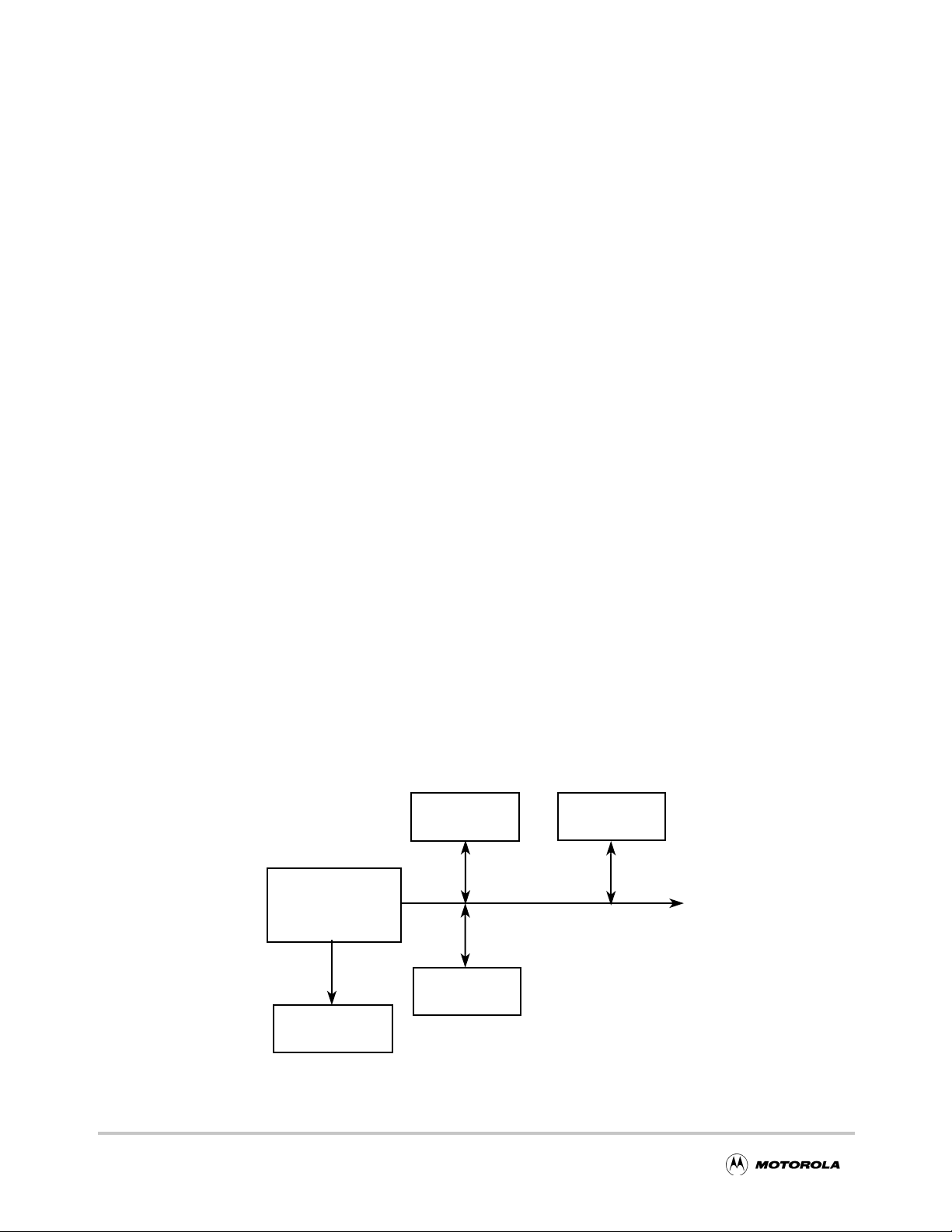
The MPC180 works well in most load/store, memory-mapped systems. An external
processor may execute application code from its R OM and RAM, using RAM and optional
non-volatile memory (such as EEPR OM) for data storage. Figure 1-1 shows an e xample of
the MPC180 in an MPC8xx system, and Figure 1-2 shows the MPC180 connected to the
local bus of the MPC826x. In these examples, the MPC180 resides in the memory map of
the processor; therefore, when an application requires cryptographic functions, it reads and
writes to the appropriate memory location in the security processor.
EEPROM
MPC860
MPC180
System Bus
1-2
SDRAM
I/O or Network
Interface
Figure 1-1. Typical MPC8xx System Example
MPC180LMB Security Processor User’s Manual
Page 15
Architectural Overview
EEPROM
SDRAM
DIMMs
60x Bus
MPC8260
SDRAM
I/O or Network
Interface
MPC180
Local Bus
SDRAM
Figure 1-2. Typical MPC8260 System Example
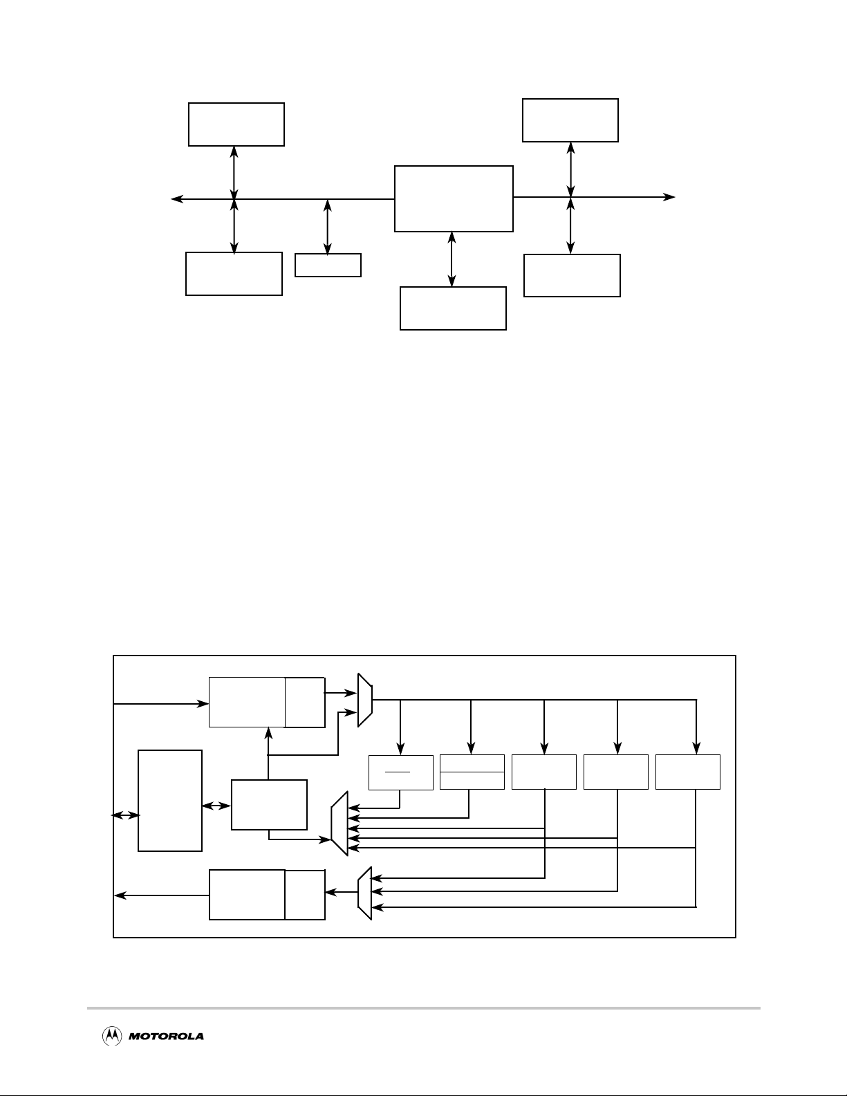
1.3 Architectural Overview
The MPC180 has a slave interface to the MPC8xx system b us and MPC8260 local b us and
maps into the host processor’s memory space. Each encryption algorithm is mapped to a
unique address space. To perform encryption operations, the host reads and writes to the
MPC180 to setup the execution unit and, then, transfers data to the execution unit directly
or through the external bus interface.
In FIFO mode, the MPC180 accepts data into the 4-Kbit input buffer and returns b urst data
through the output buffer. In this way, the host can automatically transfer bulk data
through a given EU. This minimizes host management overhead and increases overall
system throughput. Once the host configures the external bus interface (EBI), it receives
an interrupt only after all data has been transferred or processed by the MPC180.
DMA Request
8xx/6xx
I/F
(Slave)
External Bus Interface
DMA Request
INPUT
4K bit
FIFO
Controller
OUTPUT
4K bit
FIFO
DMA
Logic
DMA
Logic
RSA
ECC
SHA-1
MD 5
DES/
3DES
ARC4
RNG
Figure 1-3. MPC180 Block Diagram
Chapter 1. Overview 1-3
Page 16

Architectural Overview
The interrupt controller organizes hardware interrupts coming from individual EUs into a
single maskable interrupt, IRQ_B, for the host processor. Multiple internal interrupt
sources are logically ORed to create a single, non-prioritized interrupt for the host
processor. The controller lets the host read the unmasked interrupt source status as well as
the request status of masked interrupt sources, thereby indicating whether a given
unmasked interrupt source will generate an interrupt request to the host processor.
1.3.1 Public Key Execution Unit (PKEU)
The PKEU is capable of performing many advanced mathematical functions to support
RSA and Diffie-Hellman as well as ECC in both F 2 m (polynomial-basis) and F p. The
accelerator supports all levels of functions to assist the host microprocessor in performing
its desired cryptographic function. For example, at the highest level, the accelerator
performs modular exponentiations to support RSA and point multiplies to support ECC. At
lower levels, the PKEU can perform simple operations such as modular multiplies.
1.3.2 Data Encryption Standard Execution Unit (DEU)
The DEU is used for bulk data encryption. It can also execute the Triple-DES algorithm,
which is based on DES. The host processor supplies data to the DEU as input, and this
data is encrypted and made available for reading. The session key is input to the DEU
prior to encryption. The DEU computes the data encryption standard algorithm (ANSI
X3.92) for bulk data encryption and decryption.
DES is a block cipher that uses a 56-bit key to encrypt 64-bit blocks of data, one block at a
time. DES is a symmetric algorithm; therefore, each of the two communicating parties
share the same 56-bit key. DES processing begins after this shared session key is agreed
upon. The message to be encrypted (typically plain text) is partitioned into n sets of 64-bit
blocks. Each block is processed, in turn, by the DES engine, producing n sets of encrypted
(ciphertext) blocks. Decryption is handled in the rev erse manner. The ciphertext blocks are
processed one at a time by a DES module in the recipient’s system. The same key is used,
and the DEU manages the key processing internally so that the plaintext blocks are
recovered.
The DES/3DES execution unit supports the following modes:
• ECB (electronic code book)
• CBC (cipher block chaining)
In addition to these modes, the DEU can compute T riple-DES. Triple-DES is an extension
to the DES algorithm in which every 64-bit input block is processed three times. There are
several ways that Triple-DES can be computed. The DES accelerator on the MPC180
supports two key (K1, K2, K1) or three key (K1, K2, K3) Triple-DES.
THe MPC180 supports two of the modes of operation defined for Triple-DES (see draft
ANSI Standard X9.52-1998):
• TECB (Triple DES analogue of ECB)
1-4 MPC180LMB Security Processor User’s Manual
Page 17

Architectural Overview
• TCBC (Triple DES analogue of CBC)
1.3.3 Arc Four Execution Unit (AFEU)
The AFEU processes an algorithm that is compatible with the RC4 stream cipher from
RSA Security, Inc. The RC4 algorithm is byte-oriented; therefore, a byte of plaintext is
encrypted with a key to produce a byte of ciphertext. The key is variable length, and the
AFEU supports 40-bit to 128-bit key lengths, providing a wide range of security levels.
RC4 is a symmetric algorithm, so each of the two communicating parties share the same
key .
AFEU processing begins after this shared session key is agreed upon. The plaintext
message to be encrypted is logically partitioned into n sets of 8-bit blocks. In practice, the
host processor groups 4 bytes at a time into 32-bit blocks and write that data to the AFEU.
The AFEU internally processes each w ord one byte at a time. The AFEU engine processes
each block in turn, byte by byte, producing n sets of encrypted (ciphertext) blocks.
Decryption is handled in the reverse manner. The ciphertext blocks are processed one at a
time by an AFEU in the recipient’s system. The same key is used, and the AFEU manages
the key processing internally so that the plaintext blocks are recovered.
The AFEU accepts data in 32-bit words per write cycle and produces 4 bytes of ciphertext
for every 4 bytes of plaintext. Before any processing occurs, the key data is written to the
AFEU, after which an initial permutation on the key happens internally. After the initial
permutation is finished, processing on 32-bit words can begin.
1.3.4 Message Authentication Unit (MAU)
The MAU can perform SHA-1, MD5 and MD4, three of the most popular public message
digest algorithms. At its simplest, the MAU receives 16 32-bit registers containing a
message, and produces a hashed message of 128 bits for MD4/MD5 and 160 bits for
SHA-1. The MAU also includes circuitry to automate the process of generating an HMAC
(hashed message authentication code) as specified by RFC 2104. The HMAC can be built
upon any of the hash functions supported by MAU.
1.3.5 Random Number Generator (RNG)
Because many cryptographic algorithms use random numbers as a source for generating a
secret value, it is desirable to have a private RNG for use by the MPC180. The anonymity
of each random number must be maintained, as well as the unpredictability of the next
random number. The private RNG allows the system to develop random challenges or
random secret keys. The secret key can thus remain hidden from even the high-level
application code, providing an added measure of physical security. The RNG is also useful
for digital signature generation.
The RNG is a digital integrated circuit capable of generating 32-bit random numbers. It is
designed to comply with FIPS-140 standards for randomness and non-determinism. The
RNG creates an unpredictable sequence of bits and assembles a string of those bits into a
register. The random number in that register is accessible to the host through the host
Chapter 1. Overview 1-5
Page 18

Architectural Overview
interface of the RNG.
1.3.6 Software and Hardware Support
Customers will have access to device drivers integrated with the WindRiver VxWorks OS.
Sample drivers will also be provided to customers wishing to integrate MPC180 support
into other operating systems.
Third-party support for the MPC180 includes a development system for both the MPC860
and the MPC8260. The WindRiver/EST SBC8260C development system and Zephyr
Engineering ZPC860C, both of which include a board support package, are available to
accelerate customer design cycles.
1-6 MPC180LMB Security Processor User’s Manual
Page 19

Chapter 2
Signal Descriptions
This chapter provides a pinout diagram and signal descriptions for the MPC180 security
processor.
2.1 Signal Descriptions
Table 2-1 groups pins by functionality.
Table 2-1. Pin Descriptions
Signal name
A[18:29] 62, 64, 66,
D[0:31] 1, 2, 4, 6, 7,
CS
R/W
URST 55 I Burst Transaction. Active low signal used in the 8260 interface that indicates when
B
Pin
locations
67, 68, 70,
72–75, 77,
78
9, 11, 12,
14, 16-18,
20, 22, 24,
28–32, 34,
36, 37, 38,
87, 89, 90,
92, 94, 96,
98, 99
56 I Chip Select. Active low signal that indicates when a data transfer is intended for
54 I Read/Write. Read/write line
Signal
type
Signal pins
I Address—address bus from the processor core. These bits are decoded in the
MPC180 to produce the individual module select lines to the execution units. Note
that the processor address bus might be 32 bits wide, while the MPC180 address
bus is only 12 bits wide.
msb = bit 0
lsb = bit 31
I/O Data—bidirectional data bus. This bus is connected directly to the processor core.
msb = bit 0
lsb = bit 31
the MPC180.
1 read cycle
0 write cycle
the current read/write is a burst transfer.
Description
TS
53 I Transfer Start. Transfer start pin for control port. This signal is asserted by the
850/860 to indicate the start of a bus cycle that transfers data to or from the
MPC180. This is used by the MPC180 along with CS
transfer.
Chapter 2. Signal Descriptions 2-1
, R/W, and A to begin a
Page 20

Signal Descriptions
Table 2-1. Pin Descriptions (Continued)
Signal name
PSDVAL 82 I Data valid. This active low signal is ignored when CONFIG=0 (MPC860 Mode), but
T
A /
LUPMWAIT
RESET
CONFIG 57 I Configuration. Input that indicates whether the interface is to an MPC860 or
ENDIAN 40 I Endian. Active high for big endian mode. Low for little endian mode.
IRQ
Pin
locations
61 O Transfer Acknowledge. This active low signal is used in 860 mode and is asserted
52 I Reset. Asynchronous reset signal for initializing the chip to a known state. It is
85 O Interrupt Request. Interrupt line that signifies that one or more execution units
Signal
type
Description
is active in MPC8260 Mode. The assertion of PSD
valid on the data bus.
by the MPC180 when a successful read or write has occurred.
Local UPM wait. This active high signal is used in 8260 mode and is asserted to
indicate the number of wait states for a transaction.
Miscellaneous pins
highly recommended that this signal be connected to a dual hardware/software
reset function. Thus, the system designer can reset the MPC180 chip with optimal
flexibility.
MPC8260
1 8260 interface
0 860 interface
1 big endian
0 little endian
modules has asserted its IRQ
hardware interrupt.
VAL indicates that a data beat is
NC 26, 27, 49,
50, 51, 76,
100
DREQ1 83 O DMA Request 1. Active high signal which indicates that either the input or output
DREQ2 84 O DMA request 2. Active high signal which indicates that either the input or output
CLK 59 I Master clock input
TCK 47 I JTAG test clock
TDI 48 I JTAG test data input
TDO 44 I JTAG test data output
TMS 46 I JTAG test mode select
TRST
45 I JTAG test reset
— No connection to the pin
DMA Hardware Handshake pins
buffer is requesting data transfer by the host or DMA controller. DREQ1 and
DREQ2 are each programmable to refer to the MPC180 chip input buffer or output
buffer. This signal is designed to interoperate with a PowerQUICC IDMA channel.
buffer is requesting data transfer by the host or DMA controller. DREQ1 and
DREQ2 are each programmable to refer to the MPC180 Chip input b uff er or output
buffer. This signal is designed to interoperate with a PowerQUICC IDMA channel.
Clock
Test
2-2 MPC180LMB Security Processor User’s Manual
Page 21

Table 2-1. Pin Descriptions (Continued)
Signal Descriptions
Signal name
IVDD 10, 21, 41,
OVDD 5, 15, 25,
OVSS 3, 13, 23,
IVSS 8, 19, 39,
Pin
locations
60, 71, 93
35, 43, 65,
81, 88, 97
33, 42, 63,
79, 80, 86,
95
58, 69, 91
Signal
type
Power and Ground
I +1.8 Volts (power pins for core logic)
I +3.3 Volts (Power pins for I/O pads)
I 0 V olts (Ground)
I 0 V olts (Ground)
Description
Chapter 2. Signal Descriptions 2-3
Page 22

Signal Descriptions
Figure 2-1 shows the MPC180 pinout.
D29 1
D21 2
OVSS 3
D13
OVDD 5
D5
D28
IVSS 8
D20
IVDD 10
D12
D4
OVSS 13
D27
OVDD 15
D19
D11 17
D3
IVSS 19
D26
IVDD 21
D18
OVSS 23
D10 24
OVDD
4
6
7
9
11
12
14
16
18
20
22
25
NC
100
26
D6
99
D14
98
27
OVDD
97
28
D22
96
OVSS
95
D30
94
IVDD
93
D7
92
IVSS
91
D1590D23
89
OVDD
88
MPC180 Pinout
29
30D931
32
33
34
35
36
37
38
D31
87
39
OVSS
86
40
DREQ2
IRQ
85
848382
41
42
VAL
PSD
DREQ1
43
44
OVDD
81
45
OVSS
80
46
OVSS
79
47
A29
78
48
A28
77
49
NC
76
75
A27
A2674
A2573
A2472
IVDD71
A2370
IVSS69
A2268
A2167
A2066
OVDD65
A1964
OVSS63
A18
62
61
TA / LUPMWAIT
60
IVDD
CLK
59
IVSS
58
CONFIG
57
CS56
BURST55
54
R/W
53
TS
52
RESET
51
NC
50
NC
NC
D2
D25
D17
D1
OVSS
D24
OVDD
D16
D8
D0
IVSS
IVDD
OVSS
ENDIAN
OVDD
TDO
TMS
TRST
Figure 2-1. MPC180 Pin Diagram
2-4 MPC180LMB Security Processor User’s Manual
TCK
TDI
NC
NC
Page 23

Chapter 3
External Bus Interface and Memory Map
This chapter describes the MPC180 address map, the External Bus Interface (EBI), and EBI
registers.
3.1 Execution Unit Registers
Each MPC180 execution unit has a dedicated set of registers. The MPC180 has a unified
memory map that allows software addressibility to all internal registers. Figure 3-1 lists
each MPC180 register and its 12-bit MPC180 chip address.
A00
A40
A80
B00
B01
B02
B03
B04
B05
B06
B07
B08
B09
000
010
015
016
017
018
PKEU
BRAM [64x32]
ARAM [64x32]
NRAM[64x32]
EXP(k)
Control [CR]
Status [SR]
Mask [MR]
Instruction [IR]
Prog. counter [PC]
Clear interrupt
Modulus size
EXP(k) size
Device ID
MDEU
MDMB [0–15]
Digest [0–4]
Control [CR]
Status [SR]
Clear interrupt
Device ID
200
201
202
203
204
205
206
207
208
209
20A
20B
20C
20D
20E
600
602
DEU
Control
Status
Key1-right
Key1-left
Key2-right
Key2-left
Key3-right
Key3-left
IV-right
IV-left
DATAIN_R
DATAIN_L
DATAOUT_R
DATAOUT_L
Configuration
RNG
Command/status
AutoRand output
A00
A80
B00
B01
B02
B03
B04
B05
B06
400
401
402
403
404
408
409
40A
40B
410
EBI
Input buffer
Output buffer
CSTAT
ID register
IMASK
IBCTL
IBCNT
OBCTL
OBCNT
AFEU
Control
Status
Clear interrupt
Key length
Key data[0–3]
Last sub msg
Plaintext-in
Ciphertext-out
Context I/J
Context SBox[0–63]
Figure 3-1. MPC180 Execution Unit Registers
Chapter 3. External Bus Interface and Memory Map 3-1
Page 24

Address Map
Most of these registers are read and write, however some have special permissions. See
Table 3-1 for more information. The 12-bit MPC180 address of each register is shown ne xt
to the register name. All registers are assumed to be 32 bits wide; however, registers that
contain fewer bits will return 0 (or a known value) on unused bits for that bus transaction
only. Many registers contain multiple 32-bit words. If so, the number of words in the
register set is shown in brackets after the name. Indi vidual e x ecution unit chapters describe
how to use these registers, the bit assignments, and bit ordering.
3.2 Address Map
Table 3-1 lists the addresses for all registers in each execution unit. The 12-bit MPC180
address bus value is shown along with a 32-bit host processor address bus value.
Table 3-1. 32-Bit System Address Map
MPC180 12-Bit Address Processor 32-Bit Address Register Type
MDEU: 0x000–0x1FF
0x000 0x0000_0000 Message buffer(MB0) W
0x001 0x0000_0004 Message buffer(MB1) W
0x002 0x0000_0008 Message buffer(MB2) W
0x003 0x0000_000C Message buffer(MB3) W
0x004 0x0000_0010 Message buffer(MB4) W
0x005 0x0000_0014 Message buffer(MB5) W
0x006 0x0000_0018 Message buffer(MB6) W
0x007 0x0000_001C Message buffer(MB7) W
0x008 0x0000_0020 Message buffer(MB8) W
0x009 0x0000_0024 Message buffer(MB9) W
0x00A 0x0000_0028 Message buffer(MB10) W
0x00B 0x0000_002C Message buffer(MB11) W
0x00C 0x0000_0030 Message buffer(MB12) W
0x00D 0x0000_0034 Message buffer(MB13) W
0x00E 0x0000_0038 Message buffer(MB14) W
0x00F 0x0000_003C Message buffer(MB15) W
0x010 0x0000_0040 Message digest (MA) R/W
0x011 0x0000_0044 Message digest (MB) R/W
0x012 0x0000_0048 Message digest (MC) R/W
0x013 0x0000_004C Message digest (MD) R/W
0x014 0x0000_0050 Message digest (ME) R/W
0x015 0x0000_0054 Control (MCR) R/W
0x016 0x0000_0058 Status (MSR) R/W
0x017 0x0000_005C Clear interrupt (MCLRIRQ) W
3-2 MPC180LMB Security Processor User’s Manual
Page 25

Address Map
Table 3-1. 32-Bit System Address Map (Continued)
MPC180 12-Bit Address Processor 32-Bit Address Register Type
0x018 0x0000_0060 Version Identification (MID) R
DEU: 0x200–0x3FF
0x200 0x0000_0800 Control (DCR) R/W
0x201 0x0000_0804 Status (DSR) R
0x202 0x0000_0808 Key1_R R/W
0x203 0x0000_080C Key1_L R/W
0x204 0x0000_0810 Key2_R R/W
0x205 0x0000_0814 Key2_L R/W
0x206 0x0000_0818 Key3_R R/W
0x207 0x0000_081C Key3_L R/W
0x208 0x0000_0820 IV_R R/W
0x209 0x0000_0824 IV_L R/W
0x20A 0x0000_0828 DATAIN_R R/W
0x20B 0x0000_082C DATAIN_L R/W
0x20C 0x0000_0830 DATAOUT_R R
0x20D 0x0000_0834 DATAOUT_L R
0X20E 0x0000_0838 Configuration (DCFG) R/W
AFEU: 0x400–0x5FF
0x400 0x0000_1000 Control W
0x401 0x0000_1004 Status R
0x402 0x0000_1008 Clear interrupt W
0x403 0x0000_100C Key Length W
0x404 0x0000_1010 Key Low W
0x405 0x0000_1014 Key Lower-Middle W
0x406 0x0000_1018 Key Upper-Middle W
0x407 0x0000_101C Key Upper W
0x408 0x0000_1020 Message Byte Double Word W
0x409 0x0000_1024 Plaintext-in W
0x40A 0x0000_1028 Ciphertext-out R
0x40B 0x0000_102C S-box I/J R/W
0x410 0x0000_1040 SBox [0] R/W
0x414 0x0000_1050 SBox [1] R/W
0x418 0x0000_1060 SBox [2] R/W
... ... ... ...
0x50C 0x0000_1430 SBox [63] R/W
Chapter 3. External Bus Interface and Memory Map 3-3
Page 26

External Bus Interface
Table 3-1. 32-Bit System Address Map (Continued)
MPC180 12-Bit Address Processor 32-Bit Address Register Type
0x600 0x0000_1800 Status R
0x602 0x0000_1808 Random output R
0x800 0x0000_2000 Input buffer[128] R/W
0x880 0x0000_2200 Output buffer[128] R/W
0x900 0x0000_2400 CSTAT R/W
0x901 0x0000_2404 ID R
0x902 0x0000_2408 IMASK R/W
0x903 0x0000_240C IBCTL R/W
0x904 0x0000_2410 IBCNT R/W
0x905 0x0000_2414 OBCTL R/W
0x906 0x0000_2418 OBCNT R/W
RNG: 0x600–0x7FF
EBI: 0x800–0x9FF
PKEU: 0xA00–0xBFF
0xA00 0x0000_2800 BRAM R/W
0xA40 0x0000_2900 ARAM R/W
0xA80 0x0000_2A00 NRAM R/W
0xB00 0x0000_2C00 EXP(k) R/W
0xB01 0x0000_2C04 Control R/W
0xB02 0x0000_2C08 Status R
0xB03 0x0000_2C0C Interrupt mask R/W
0xB05 0x0000_2C14 Program counter R/W
0xB06 0x0000_2C18 Clear interrupt (CLRIRQ) W
0xB07 0x0000_2C1C Modulus size R/W
0xB08 0x0000_2C20 EXP(k) size R/W
0xB09 0x0000_2C24 Device ID R/W
3.3 External Bus Interface
The EBI handles the interface between the processor and MPC180’s internal execution
units. It has the following features:
• Memory-mapped data transfers to/from the host to the MPC180 in single, burst, or
DMA modes
• 4-Kbit input and output buffers that allows the host to set up an operation and pass
control of interrupts and data flow to the MPC180 until the operation completes
3-4 MPC180LMB Security Processor User’s Manual
Page 27

External Bus Interface
• Automatic buffer filling and emptying. DREQ1 and DREQ2 stay asserted as long as
memory space or data is in the buffers, letting the host load data for the next
operation before the current operation finishes
• Interrupt routing and masking, which lets the host individually detect interrupts
• Interrupt auto-unmask, which lets the controller unmask an interrupt to the host
when an operation finishes
3.3.1 EBI Registers
Table 3-2 describes the controller’s se v en 32-bit, host-addressable re gisters that are used to
program MPC180.
Table 3-2. EBI Registers
Name R/W Description
CSTAT R/W Command/Status Register. Used to control global MPC180 functions and to monitor interrupts (see
Section 3.3.1.1, “Command/Status Register (CSTAT)”).
ID R ID. Gives the fixed ID number unique to the MPC180 (see Section 3.3.1.2, “ID Register”).
IMASK R/W Interrupt Mask Register. Allows the masking of interrupts to the host (see Section 3.3.1.3, “IMASK
Register”).
IBCTL R/W Input Buffer Control Register. Contains the starting address in the MPC180 where data from the
input buffer is to be written. Contains the counter mask field (see Section 3.3.1.4, “Input Buffer
Control (IBCTL) and Output Buffer Control (OBCTL) Registers”).
IBCNT R/W Input Buffer Count Register. Gives the total number of 32-bit words to be written to a specific
execution unit for a given operation. This number is not limited to 128 (4 Kbits), but is the total
number of words to be taken from the input buffer and written to the selected execution unit (see
Section 3.3.1.5, “Input Buffer Count (IBCNT) and Output Buffer Count (OBCNT) Registers”).
OBCTL R/W Output Buffer Control Register. Contains the starting address in the MPC180’s address map from
where data should be transferred to the output buffer. Also contains the counter mask field (see
Section 3.3.1.4, “Input Buffer Control (IBCTL) and Output Buffer Control (OBCTL) Registers”).
OBCNT R/W Output Buffer Count Register. Contains the total number of 32-bit words a specific execution unit is
to write to the output buffer for a given operation. This number is not limited to 128 (4 Kbits), but is
the total number of words to be read from the selected (or enabled) execution unit (see
Section 3.3.1.5, “Input Buffer Count (IBCNT) and Output Buffer Count (OBCNT) Registers”).
3.3.1.1 Command/Status Register (CSTAT)
CSTAT, shown in Figure 3-2, is used to control the chip software reset and auto-unmask
function and to report interrupt status. The controller synchronizes the software reset
function to the rising edge of MCLK, guaranteeing sufficient setup and hold times. Note
that after the CSTAT register is read, bits 18-23 will be cleared, thus not allowing bitwise
operations on these bits.
Chapter 3. External Bus Interface and Memory Map 3-5
Page 28

External Bus Interface
05678101112131415
Field — DR2C DR1C — DEU AFEU MDEU RNG PKEU
Reset 0000_0000_0000_0000
R/W R/W
16 17 18 19 20 21 22 23 24 27 28 30 31
Field DR2A DR1A DEU AFEU MDEU RNG PKEU MPC180 Destination AUTO-UNMASK RST
Reset 0000_0000_0000_0000
R/W R/W
Addr 0x900
Figure 3-2. Command/Status Register (CSTAT)
Table 3-3 describes CSTAT fields.
Table 3-3. CSTAT Field Descriptions
Bits Name Description
0–5 — Reserved, should be cleared.
6 DR2C DREQ2 Control Bit
0 = DREQ2 displays the state of the output FIFO
1 = DREQ2 displays the state of the input FIFO
7 DR1C DREQ1 Control Bit
0 = DREQ1 displays the state of the input FIFO
1 = DREQ1 displays the state of the output FIFO
8–10 — Reserved, should be cleared.
11–15 Source interrupt indicators for the individual execution units. These are the masked interrupts from the
execution units.
For bits 11–15:
0 interrupt not pending
1 interrupt pending
11 DEU Data Encryption Standard Execution Unit External Bus Interface interrupts
12 AFEU Arc Four Execution Unit External Bus Interface interrupts
13 MDEU Message Digest Execution Unit External Bus Interface interrupts
14 RNG Random Number Generator External Bus Interface interrupts
15 PKEU Public key Execution Unit External Bus Interface interrupts
16 DR2A DREQ2 Activation
0 = Inactive
1 = Active
17 DR1A DREQ1 Activation
0 = Inactive
1 = Active
18–22 Raw interrupt indicators for individual execution units. These are the unmasked interrupts from the
execution units.
For bits18–22:
0 interrupt not pending
1 interrupt pending
3-6 MPC180LMB Security Processor User’s Manual
Page 29

External Bus Interface
Table 3-3. CSTAT Field Descriptions
Bits Name Description
18 DEU Data Encryption Standard Execution Unit interrupts
19 AFEU Arc Four Execution Unit interrupts
20 MDEU Message Digest Execution Unit interrupts
21 RNG Random Number Generator interrupts
22 PKEU Public key Execution Unit interrupts
23 MPC180 MPC180 IRQ. This bit, when set, indicates an interrupt is pending in the MPC180.
0 interrupt not pending
1 interrupt pending
24–27 Destination Destination bits. Only one execution unit on MPC180 can be active at a time through FIFO
accesses, so the host must program CSTAT to enable the appropriate execution unit. The
host must guarantee that all data related to a specific operation has been processed before
updating CSTAT, otherwise unpredictable results occur in MPC180 because the controller
acts on one execution unit at a time.
1000 DEU
1001 AFEU
1010 MDEU
1011 RNG
1100 PKEU
0xxx no active module
28–30 AUTO-
UNMASK
31 RST Software reset. Performs the same function as asserting RESET
Auto-unmask bit. Enables or disables the auto-unmask function. This function is used to
unmask an interrupt from the currently active execution unit. It is to be used when a
execution unit sends a series of intermediate interrupts the host does not want to see. For
example, if the DEU is enabled and active, many interrupts may be generated for
intermediate results. The host, however, may only be interested in the final interrupt that
occurs when the DEU completes processing all of the data. To begin the operation, the host
masks off the interrupts from the DEU and then writes to the auto-unmask bit. Then, when
the DEU completes processing all the data, the controller unmasks the DEU interrupt and
allows the final DEU interrupt (signaling the completion of processing) to be sent to the host.
The host can then read CSTAT to determine that the DEU generated an interrupt and take
appropriate action.
for bits 28–30:
000 disabled
001 enabled
on MPC180. Setting this
bit resets the MPC180 within two MCLK cycles; the controller clears this bit.
0—
1 chip reset
The complete MPC180 register map, including all execution units, is available to the host.
Although the host can access control registers and input and output buffers while an
instruction is executing, it cannot access the execution unit itself.
3.3.1.2 ID Register
Figure 3-3 shows the ID register. Note that the ID register contains a 32-bit value that
identifies the version of MPC180. Its value at reset is 0x0065_1491and should be read with
the ENDIAN mode set to big endian.
Chapter 3. External Bus Interface and Memory Map 3-7
Page 30

External Bus Interface
0 7 8 1011 131415
Field — MPC180 MDEU DEU
Reset 0000_0000 011 0_01 01
R/W Read
16 17 19 20 22 23 25 26 28 29 31
Field DEU AFEU RNG — EBI PKEU
Reset 0 001 001 0_10 01_0 001
R/W Read
Addr 0x901
Figure 3-3. ID Register
Table 3-4 describes the ID fields.
Table 3-4. ID Field Descriptions
Bits Name Description
0–7 — Reserved, should be cleared.
8–10 MPC180 MPC180 version number.
11–13 MDEU Message Digest Execution Unit version number
14–16 DEU Data Encryption Standard Execution Unit version number
17–19 AFEU Arc Four Execution Unit version number
20–22 RNG Random Number Generator version number
23–25 — Reserved, should be cleared.
26–28 EBI Controller version number
29–31 PKEU Public key Execution Unit version number
3.3.1.3 IMASK Register
The built-in interrupt controller (IRQ module) gathers all execution unit interrupt signals
and presents one output (IRQ
interrupts from execution units by programming the IMASK register . In this w ay , interrupts
can be controlled from a single source. Some execution-unit-specific configuration is
required to ensure proper response to any interrupt. The user can read the appropriate
address in CSTAT to get the interrupt status of all execution units at once.
The interrupt port consists of the IRQ
all pending interrupts from the execution units.
) to the host. It also lets the user selectively mask or disable
output, which is negated after the host responds to
All interrupts from the execution units have the same priority. Figure 3-4 shows the bit
assignments in the IRQ register for all the MPC180 execution units. All enable (mask)
registers operate on the corresponding bits. An interrupt is masked when its corresponding
IMASK bit is a 1.
3-8 MPC180LMB Security Processor User’s Manual
Page 31

External Bus Interface
0 15
Field —
Reset 0000_0000_0000_0000
R/W R/W
16 26 27 28 29 30 31
Field — DEU AFEU MDEU RNG PKEU
Reset 0000_0000_0000_0000
R/W R/W
Addr 0x902
Figure 3-4. IMASK Register
Table 3-5 describes the IMASK fields.
Table 3-5. IMASK Field Descriptions
Bits Name Description
0–26 — Reserved, should be cleared.
27 DEU Data Encryption Standard Execution Unit global interrupt control
0 interrupt unmasked
1 interrupt masked
28 AFEU Arc Four Execution Unit global interrupt control
0 interrupt unmasked
1 interrupt masked
29 MDEU Message Digest Execution Unit global interrupt control
0 interrupt unmasked
1 interrupt masked
30 RNG Random Number Generator global interrupt control
0 interrupt unmasked
1 interrupt masked
31 PKEU Public key Execution Unit global interrupt control
0 interrupt unmasked
1 interrupt masked
3.3.1.4 Input Buffer Control (IBCTL) and Output Buffer Control
(OBCTL) Registers
The IBCTL register is used to control the input buffer starting address and address
increment function.
The OBCTL register is used to control the output buffer starting address and address
increment function.
Chapter 3. External Bus Interface and Memory Map 3-9
Page 32

External Bus Interface
Figure 3-5 shows both the IBCTL and the OBCTL registers.
07815
Field — Count Mask
Reset 0000_0000_0000_0000
R/W R/W
16 19 20 31
Field — Starting Address
Reset 0000_0000_0000_0000
R/W R/W
Addr IBCTL: 0x903; OBCTL: 0x905
Figure 3-5. Input Buffer Control (IBCTL) and Output Buffer Control (OBCTL)
Registers
Table 3-6 describes IBCTL fields.
Table 3-6. IBCTL Field Descriptions
Bits Name Description
0–7 — Reserved, should be cleared.
8–15 Count mask Defines how the buffer controller presents addresses to execution units when data is
taken from the input buffer. The count mask bits define the number of 32-bit words to be
transferred into each execution unit as defined by the input block size upon which the
specific algorithms operate.
16–19 — Reserved, should be cleared.
20–31 Starting address Starting address of the input buffer data destination. The starting address is the internal
offset to which the first word of data from the input buffer is written for a given operation.
All subsequent addresses are derived from this address.
Table 3-7 describes OBCTL fields.
Table 3-7. OBCTL Register Field Descriptions
Bits Name Description
0–7 — Reserved, should be cleared.
8–15 Count mask Defines how the buffer controller presents addresses to execution units when data is
read from the active execution unit and written to the output buffer. The count mask bits
define the number of 32-bit words to be transferred from each execution unit as defined
by the output block size produced by the specific algorithms.
16–19 — Reserved, should be cleared.
20–31 Starting address Starting address of the output buffer data source. The starting address is the internal
offset from which the first word of data to the output buffer is read for a given operation.
All subsequent addresses are derived from this address.
3-10 MPC180LMB Security Processor User’s Manual
Page 33

EBI Controller Operation
3.3.1.5 Input Buffer Count (IBCNT) and Output Buffer Count
(OBCNT) Registers
IBCNT indicates the number of 32-bit words to be used for an operation. For example, if
the PKEU is to operate on 512 bits (16 words), IBCNT should be set to 0x0000_0010,
corresponding to sixteen, 32-bit words to be taken from the input buffer and written to the
PKEU.
When the input buffer counter reaches its terminus, IBCNT = 0, indicating that the number
of words transferred to the active execution units matches the IBCNT value, data transfer
stops automatically.
OBCNT contains the number of 32-bit words expected to be read for a particular operation.
For example, if the DEU module is to operate on 512 bits, OBCNT should be set to
0x0000_0010, corresponding to sixteen 32-bit words to be read from the DEU module and
written to the output buffer.
Figure 3-6 shows the IBCNT and OBCNT registers.
0 31
Field Count
Reset 0000_0000_0000_0000_0000_0000_0000_0000
R/W R/W
Addr IBCNT: 0x904; OBCNT: 0x906
Figure 3-6. Input Buffer Count (IBCNT) and Output Buffer Count (OBCNT)
Registers
3.4 EBI Controller Operation
The controller (EBI) is the interface between the host, the input and output FIFOs, and the
individual execution units. It also contains control logic designed to help off load flow
control from the host. The controller facilitates single access or burst reads and writes from
the host, and it also manages the interrupts that execution units send to the host. The
controller also controls DREQ1
to and from the buffers.
The MPC180 EBI supports the MPC860 or MPC8260 processor interface, depending on
the static state of the external pin CONFIG. When CONFIG is 0, the MPC180 interface is
MPC860-compatible. When CONFIG is 1, the MPC180 interface is MPC8260-compatible.
Burst access is only supported to/from the input and output FIFOs in MPC8260 mode. In
MPC8260 mode, the MPC180 always assumes bursts to be eight 32-bit words.
and DREQ2, which can be used to signal DMA transfers
3.4.1 Buffer Accesses (FIFO Mode)
The controller contains an input buffer and an output b uffer of 4096 bits each. These buffers
can be written to directly by the host or by using DMA. For direct access, the host simply
Chapter 3. External Bus Interface and Memory Map 3-11
Page 34

EBI Controller Operation
writes or reads the address of the buffer.
DREQ1
and DREQ2 (input/output buffer ready) are programmable handshak e signals used
for buffer control. An external DMA controller can use this handshake to service the input
or output buffer with data transfers as required. The EBI CSTAT register determines
whether these signals reflect the state of the input buffer or output buffer. By default,
DREQ1
refers to the state of the input buffer and DREQ2 refers to the state of the output
buffer.
NOTE:
DREQx
refers to either DREQ1 or DREQ2. Either can be
programmed to refer to the state of the input or output buffer.
In FIFO mode, the input buffer automatically fills and the output buffer automatically
empties. In the input buffer, this is accomplished by assertion of DREQx
whenev er at least
eight 32-bit words (in MPC8260 mode) of space are available. Similarly, for the output
buffer, DREQx
remains asserted as long as at least eight 32-bit words (MPC8260 mode)
are in the output buffer to be read.
3-12 MPC180LMB Security Processor User’s Manual
Page 35

Chapter 4
Data Encryption Standard Execution
Unit
This chapter explains how to program the DEU (Data Encryption Standard Ex ecution Unit)
to encrypt or decrypt a message.
4.1 Operational Registers
All operational registers within the main control block are 32-bit addressable, howe ver they
may contain less than 32 bits. The keys, initialization v ector , plaintext and ciphertext are all
64-bit, and each takes two registers. Each has a left (most significant word) and a right (least
significant word) register. Table 4-1 lists DEU registers. These registers are described in
more detail in the following sections.
Table 4-1. Data Encryption Standard Execution Unit (DEU) Registers
MPC180 12-Bit Address Processor 32-Bit Address Register Type
0x200 0x0000_0800 Control (DCR) R/W
0x201 0x0000_0804 Status (DSR) R
0x202 0x0000_0808 Key1_R R/W
0x203 0x0000_080C Key1_L R/W
0x204 0x0000_0810 Key2_R R/W
0x205 0x0000_0814 Key2_L R/W
0x206 0x0000_0818 Key3_R R/W
0x207 0x0000_081C Key3_L R/W
0x208 0x0000_0820 IV_R R/W
0x209 0x0000_0824 IV_L R/W
0x20A 0x0000_0828 DATAIN_R R/W
0x20B 0x0000_082C DATAIN_L R/W
0x20C 0x0000_0830 DATAOUT_R R
0x20D 0x0000_0834 DATAOUT_L R
0X20E 0x0000_0838 Configuration (DCFG) R/W
Chapter 4. Data Encryption Standard Execution Unit 4-1
Page 36

Operational Registers
4.1.1 DEU Control Register (DCR)
The control register, shown in Figure 4-1, contains static bits that define the encryption
mode of operation for the DEU. This is typically written along with the keys and
initialization vector at the start of each new encryption process. All unused bits of DCR
are read as 0 values.
0 28 29 30 31
Field — MODE XDES E/D
Reset 0000_0000_0000_0000
R/W R
Addr
0x200
R/W
Figure 4-1. DES Control Register (DCR)
Table 4-2 describes control register fields.
Table 4-2. DCR Field Descriptions
Bits Name Description
0–28 — Reserved, should be cleared.
29 MODE Selects the DES mode of operation. Both Electronic Code Book (ECB) and Cipher Block
Chaining (CBC) are supported.
0 = ECB
1 = CBC
30 XDES Controls single DES or triple DES.
0 = Single DES
1 = Triple DES
31 E/D Controls whether the input data will be encrypted or decrypted.
0 = decrypt
1 = encrypt
4.1.2 DEU Configuration Register (DCFG)
The configuration register contains two bits that are set only during hardware initialization.
All unused bits of DCFG are read as 0 values.
0 29 30 31
Field — RST IMSK
Reset 0000_0000_0000_0000
R/W R
Addr 0x20E
Figure 4-2. DEU Configuration Register (DCFG)
4-2 MPC180LMB Security Processor User’s Manual
W R/W
Page 37

Table 4-3 describes DCFG fields.
Table 4-3. DCFG Field Descriptions
Bits Name Description
0–29 — Reserved, should be cleared.
Operational Registers
30 RST The DES can be reset by asserting the RESET signal or by setting the Software Reset bit in
31 IMSK Clearing the interrupt mask bit will allow interrupts on the IRQ
the Control Register. The software and hardware resets are functionally equivalent. The
software reset bit will clear itself one cycle after being set.
0 —
1 software reset
pin. It does not aff ect the IRQ
bit in the status register. This bit is set (interrupts disabled) any time a hardware/software
reset is performed. The user must clear this bit to enable hardware interrupts.
0 enable interrupts
1 disable interrupts
4.1.3 DEU Status Register (DSR)
The status register contains bits that giv e information about the state of the DEU. There are
two bits which state when more input can be written to the input data register and read from
the output data register. T o maximize throughput, data is b uffered, and reading and writing
can be overlapped. When the IRDY bit is one, new data can be written to the input
(DATA_IN) registers. It is possible to write three 64-bit blocks of data before any output
data is read (and the IRDY signal goes low).
Figure 4-3 shows the DES status register.
0 29 30 31
Field — IDRY ORDY
Reset 0000_0000_0000_0000
R/W R
Addr 0x201
Figure 4-3. DES Status Register (DSR)
Table 4-4 describes DSR fields.
Table 4-4. DSR Field Descriptions
Bits Name Description
0–29 — Reserved, should be cleared.
30 IRDY Input Ready. Input Buffer ready to accept more data.
31 ORDY Output Ready. Output Buffer has data to send.
Upon completion of an encryption (or decryption), the ORDY signal will go high,
indicating that the output is ready to be read from the DATA_OUT registers. If interrupts
are enabled, then IRQ
will be asserted. After the ORDY signal goes high, new data in the
Chapter 4. Data Encryption Standard Execution Unit 4-3
Page 38

Operational Registers
DATA_IN registers will start processing. When completed, the resulting output will be held
in a working register until the output ciphertext is read from the DATA_OUT registers.
Then the held data will be copied to the DATA_OUT registers and the ORDY signal
asserted again. The interrupt IRQ
signal will be active as long as ODRY is asserted.
4.1.4 Key Registers
The DEU supports up to three independent 56-bit keys. Each key uses two 32-bit registers
(56 bits of key plus 8 bits of parity). Note that key parity bits are ignored in processing.
For single DES, only one key is used (K ey1_L and K ey1_R); the other tw o are ignored. For
Triple DES, all three ke ys are used. To simulate two-key T riple DES (in which the first and
third keys are identical), Key1_L and Key1_R are also written to Key3_L and Key3_R.
When using three-key triple DES, the three keys must be written in order (K e y1, K ey2, and
then Key3), otherwise the first key may overwrite the third.
The key registers are read/write and must not be written while data is being
encrypted/decrypted. Doing so will result in corrupted data.
4.1.5 Initialization Vector
The DEU supports CBC mode, which requires a 64-bit initialization vector (IV). The IV
uses two 32-bit registers (IV_L and IV_R). The IV should be written before the first block
of data is encrypted. After each block of data is encrypted, the Initialization Vector register
is updated to prepare for the next block of data. This register is readable so that the current
encryption context (mode, keys, and IV) can be saved and restored.
The Initialization Vector registers must not be written while data is being encrypted or
decrypted. Doing so will result in corrupted data.
4.1.6 DATAIN
Data to be encrypted or decrypted is written to the DATAIN registers. Data is first written
to DATAIN-R and then to DATAIN-L. DEU processing begins automatically with the
completion of the write to the DATAIN-L register.
4.1.7 DATAOUT
Processed data is stored in the DATAOUT registers. Data must be read from DATAOUT-R
first. Reading data from DATA OUT-L indicates completion of the 64-bit block read, which
allows the DEU to write the next 64 bits to DATAOUT-R and DATAOUT-L. If two 64-bit
blocks have been written to the DATAIN registers while the DATAOUT registers haven’t
been read, the DEU will stall to prevent an overwrite. IF three 64-bit blocks are written to
DATAIN before any are read from DATAOUT, the IRDY bit in the Status register will go
low, indicating that any additional blocks written to DATAIN will cause a loss of data due
to overwrite.
4-4 MPC180LMB Security Processor User’s Manual
Page 39

Chapter 5
Arc Four Execution Unit
This chapter explains how to program the AFEU (Arc Four Execution Unit) to encrypt or
decrypt a message.
5.1 Arc Four Execution Unit Registers
All operational registers within the main control block are 32-bit addressable. However,
they may contain less than 32 bits.
T able 5-1 lists AFEU registers. These re gisters are described in more detail in the following
sections.
Table 5-1. Arc Four Execution Unit (AFEU) Registers
MPC180 12-Bit Address Processor 32-Bit Address Register Type
0x400 0x0000_1000 Control W
0x401 0x0000_1004 Status R
0x402 0x0000_1008 Clear interrupt W
0x403 0x0000_100C Key Length W
0x404 0x0000_1010 Key Low W
0x405 0x0000_1014 Key Lower-Middle W
0x406 0x0000_1018 Key Upper-Middle W
0x407 0x0000_101C Key Upper W
0x408 0x0000_1020 Message Byte Double Word W
0x409 0x0000_1024 Plaintext-in W
0x40A 0x0000_1028 Ciphertext-out R
0x40B 0x0000_102C S-box I/J R/W
0x410 0x0000_1040 SBox [0] R/W
0x414 0x0000_1050 SBox [1] R/W
0x418 0x0000_1060 SBox [2] R/W
... ... ... ...
0x50C 0x0000_1430 SBox [63] R/W
Chapter 5. Arc Four Ex ecution Unit 5-1
Page 40

Arc Four Execution Unit Registers
5.1.1 Status Register
The AFEU Status Register, shown in Figure 5-1, contains seven bits of information. These
bits describe the state of the AFEU circuit and are all active-high.
0 24 25 262728293031
Field — Input Buffer
empty
Reset 0000_0000_0000_0000
R/W Read
Addr 0x401
Figure 5-1. Arc Four Execution Unit Status Register
Table 5-2 describes the AFEU Status Register fields.
Table 5-2. AFEU Status Register Field Descriptions
Bit Name Description
Full msg
done
Sub-msg
done
Permute
done
Initialize
done
IRQ Busy
0–24 — Reserved, should be cleared.
25 Input Buffer empty Set when there is no data waiting in the AFEU Input Buffer. This can be used to monitor
when the AFEU is ready to receive the next sub-message while it is processing the
current sub-message. Writing to the Message register will clear this bit.
26 Full message done Set when the last sub-message has been processed. This bit will remain set until a new
key is written. Reading from the Cipher register will clear this bit.
27 Sub-message done Set when the sub-message has been processed. Once the next sub-message is written,
the AFEU will begin processing it and this bit will clear.
28 Permute done Set once the memory is permuted with the key. Once the first sub-message is written, the
AFEU will begin processing the message and this bit will clear.
29 Initialize done Set once memory initialization is complete. Once the key data and length is written, the
AFEU will begin permuting the memory and this bit will clear.
30 IRQ Asserted whenever an interrupt is pending (if interrupts are enabled). The following
conditions will generate an interrupt:
Memory initialization done
Memory permutation done
Sub-Message processing done
Full Message processing done
The specific cause of the interrupt can be determined by reading the additional bits of the
status register.
Hardware interrupts are disabled following a reset. The IRQ bit in the status register is not
affected by masking hardware interrupts in the control register.
31 Busy Asserted whenever the AFEU core is not in an idle state. Memory initialization or
permutation and message processing conditions will cause this bit to be set. The Busy bit
will be set during context writes/reads.
5-2 MPC180LMB Security Processor User’s Manual
Page 41

Arc Four Execution Unit Registers
5.1.2 Control Register
Figure 5-2 shows the AFEU Control Register.
0 29 30 31
Field — RST IMSK
Reset 0000_0000_0000_0001
R/W W
Addr
0x400
Figure 5-2. Arc Four Execution Unit Control Register
Table 5-3 describes the AFEU Control Register fields.
Table 5-3. AFEU Control Register Field Descriptions
Bit Name Description
0–29 — Reserved, should be cleared.
30 RST The AFEU can be reset by asserting the RESET signal or by setting the Software Reset bit in the
31 IMSK Clearing the interrupt mask bit will allow interrupts on the IRQ
Control Register. The software and hardware resets are functionally equivalent. The software
reset bit will clear itself one cycle after being set.
0 —
1 software reset
pin. It does not affect the IRQ bit in
the status register. This bit is set (interrupts disabled) any time a hardware/software reset is
performed. The user must clear this bit to enable hardware interrupts.
0 enable interrupts
1 disable interrupts
5.1.3 Clear Interrupt Register
The Clear Interrupt Register is a write-only register. Writing to this register will clear the
IRQ
signal and the IRQ bit in the status register. The actual data written to this register is
ignored.
5.1.4 Key Length Register
The Key Length Register is a 4-bit write-only register that stores the number of bytes
(minus one) in the key. Writing to this register will signal the AFEU to start permuting the
memory with the key. Therefore, the key must be written before writing to this register.
5.1.5 Key (Lo w/Lower-mid dle/Upper-middle/Upper) Register
Each register is 32-bits wide (write-only). Because the key size may be 1 to 16 bytes in
length, the key data is stored in four individually addressable re gisters. The ke y low re gister
holds the lowest significant four bytes of the key. The Ke y Lower -Middle Register holds the
next lowest four bytes of the key. The Key Upper-Middle Register holds the next highest
four bytes of the key. The Key Upper Register holds the most significant four bytes of the
key .
Chapter 5. Arc Four Ex ecution Unit 5-3
Page 42

Arc Four Execution Unit Registers
NOTE:
If the key length is not divisible by four, the lower key data
registers must be filled before writing to the upper key data
registers.
5.1.6 Message Byte Double-Word Register
The Message Byte Double-Word Register is a 3-bit write-only register and is used to hold
the number of bytes (minus one) in the last/partial sub-message. A 1 in the MSB of this
register indicates to the AFEU that this is the last sub-message. Figure 5-3 shows the
Message Byte Double-Word Register. The default number of sub-message bytes is four.
028293031
Field — Last1
sub-message
Reset 0000_0000_0000_0000
# sub-message
bytes - 1
R/W
Addr
1
Setting the Last Sub-message bit in this register will cause the AFEU to reset and start initializing once the full
message is complete. The contents of the cipher register will hold the last processed sub-message.
W
0x408
Figure 5-3. Arc Four Execution Unit Message Byte Double-Word Register
5.1.7 Message Register
The Message Register is a 32-bit write-only register that stores the sub-message to be
processed. This can either be the plaintext to be encrypted or ciphertext to be decrypted.
Writing data to this register signals the AFEU to start processing the data.
5.1.8 Cipher Register
The Cipher Register is a 32-bit read-only register that stores the processed sub-message.
This can either be the encrypted ciphertext or decrypted plaintext. Data in this register is
valid when the sub- or full message done bit is set in the status register.
NOTE:
If the sub-message is less than 32-bits, the unused bits in the
Cipher Register will be the same as the corresponding bits
written to the Message Register.
5-4 MPC180LMB Security Processor User’s Manual
Page 43

Arc Four Execution Unit Registers
5.1.9 S-box I/J Register
The Sbox I/J Register is a 24-bit read/write register where the Sbox I/J pointers are stored.
The contents of this register must be read prior to context switching and must be written
back to the AFEU before resuming message processing of an interrupted message. This
register may be accessed whenever the AFEU is idle.
5.1.10 S-box0 – S-box63 Memor y
The S-box Memory consists of 64 read/write 32-bit blocks. The entire contents of the S-box
memory must be read prior to context switching and must be written back to the AFEU
before resuming message processing of an interrupted message. The S-box memory may
be accessed whenever the AFEU is idle.
Chapter 5. Arc Four Ex ecution Unit 5-5
Page 44

Arc Four Execution Unit Registers
5-6 MPC180LMB Security Processor User’s Manual
Page 45

Chapter 6
Message Digest Execution Unit
This chapter explains how to program the MDEU (Message Digest Ex ecution Unit) within
the MPC180 to hash a message for authentication.
6.1 Operational Registers
All operational registers within the MDEU are 32-bit addressable, however they may
contain less than 32 bits.
Table 6-1 lists message registers. These registers are described in more detail in the
following sections.
Table 6-1. Message Digest Execution Unit (MDEU) Registers
MPC180 12-Bit Address Processor 32-Bit Address Register Type
0x000 0x0000_0000 Message buffer(MB0) W
0x001 0x0000_0004 Message buffer(MB1) W
0x002 0x0000_0008 Message buffer(MB2) W
0x003 0x0000_000C Message buffer(MB3) W
0x004 0x0000_0010 Message buffer(MB4) W
0x005 0x0000_0014 Message buffer(MB5) W
0x006 0x0000_0018 Message buffer(MB6) W
0x007 0x0000_001C Message buffer(MB7) W
0x008 0x0000_0020 Message buffer(MB8) W
0x009 0x0000_0024 Message buffer(MB9) W
0x00A 0x0000_0028 Message buffer(MB10) W
0x00B 0x0000_002C Message buffer(MB11) W
0x00C 0x0000_0030 Message buffer(MB12) W
0x00D 0x0000_0034 Message buffer(MB13) W
0x00E 0x0000_0038 Message buffer(MB14) W
0x00F 0x0000_003C Message buffer(MB15) W
0x010 0x0000_0040 Message digest (MA) R/W
0x011 0x0000_0044 Message digest (MB) R/W
0x012 0x0000_0048 Message digest (MC) R/W
Chapter 6. Message Digest Execution Unit 6-1
Page 46

Operational Registers
MPC180 12-Bit Address Processor 32-Bit Address Register Type
0x013 0x0000_004C Message digest (MD) R/W
0x014 0x0000_0050 Message digest (ME) R/W
0x015 0x0000_0054 Control (MCR) R/W
0x016 0x0000_0058 Status (MSR) R/W
0x017 0x0000_005C Clear interrupt (MCLRIRQ) W
0x018 0x0000_0060 Version Identification (MID) R
6.1.1 MDEU Version Identification Register (MID)
The Identification Register contains a value reserved for a particular version and
configuration of the MDEU. As future hardware is developed to support dif ferent field types
or different microcode, each version will be assigned a different identifier.
The value returned is ID = 0x0001.
6.1.2 MDEU Control Register (MCR)
The control register contains static bits that define the mode of operation for the MDEU. In
addition to the static control bits, several bits are dynamic. These dynamic bits are set by a
write to the MCR initiated by the host processor and are reset automatically by the MDEU
after one cycle or operation. All unused bits of the MCR are read as 0 values.
Figure 6-1 shows the MDEU Control Register and Table 6-2 describes this register’s fields.
0 15
Field —
Reset 0000_0000
R/W R/W
16 19 20 21 22 23 24 23 26 27 28 29 30 31
Field — ENGO OPAD IPAD — MD5 MD4 RST IE GO BSWP STEP —
Reset 0000_0000
R/W R/W
Addr 0x015
Figure 6-1. MDEU Control Register (MCR)
6-2 MPC180LMB Security Processor User’s Manual
Page 47

Operational Registers
Table 6-2. MCR Field Descriptions
Bits Name Description
0–19 — Reserved, should be cleared.
20 ENGO Enables automatic start of hashing as soon as the MDMB buffers ha v e all been written. It
is not necessary to set the GO bit manually.
21 OPAD The assertion of OPAD causes:
1. The value written to the 512 bit Message Buffer to be exclusive-ORed with the outer
hash pad value
2. Unlik e IPAD, a procedur al change occurs: upon starting the hash of the value written to
the Message Buffer , the contents of the Message Digest Buffer is copied to the Message
Buffer, and is padded appropriately.
By performing the copy from MDB to MB, the step of appending the inner hash result to
the padded key is performed automatically. OPAD is autocleared upon completion of a
hash of a single message block.
22 IPAD The assertion of IPAD causes the value written to the 512 bit Message Buffer to be
exclusive-ORed with the inner hash pad v alue. This value is autocleared upon completion
of a hash of a single message block. Note that because this control bit affects the value
stored in the 512 bit message buffer, if block chaining is to be used, it should be set only
while the secret key is written to the 512 bit Message Buffer, and should be cleared
manually at the same time GO is asserted.
23 — Reserved, should be cleared.
24 MD5 The assertion of the MD5 bit signifies that an MD5 hash will be computed. If both MD4
and MD5 are not asserted, a SHA-1 Hash will be computed.
25 MD4 The assertion of the MD4 bit signifies that an MD4 hash will be computed. If both MD4
and MD5 are not asserted, a SHA-1 Hash will be computed.
26 RST The RST bit is a software reset signal. When activated, the MDEU will reset immediately,
halting any ongoing hash. All registers and buffers revert to their initial state. Normally,
asserting GO continues an existing hash function across multiple 512-bit message
blocks. Should a fresh-hash be desired for a new message block, the RST bit should be
asserted prior to loading the new message block into the Message Buffer.
27 IE The IE bit represents the Interrupt Enable flag. When set to 1, the IRQ
thus when an interrupt occurs, the IRQ
all interrupts are disabled, and the IRQ
bit acts as the global interrupt enable.
28 GO The GO bit initiates the processing of the 512 bit message currently stored in the
Message Buffer. This hash will be a continuation of any existing hash of multiple
message blocks. In order to begin a new hash, the RST bit described below should be
asserted prior to loading the new 512 bit Message Block. The 512 bit Message Block is
double-buffered; a new block of message may be written while a hash is under process. If
a new block is so written, then hashing will continue with the new block without GO
needing to be reasserted.
29 BSWP The BSWP bit causes byte-swapping of the Message Digest Buffer Registers
(MDA-MDE) as they are read out of the MDEU.
signal will be activated. When the IE bit is set to 0,
output pin will be held inactive, that is, 0. The IE
signal is enabled,
30 STEP The STEP bit allows the MDEU to be stepped through on a single clock cycle basis.
When active, that is 1, the MDEU computes one “round” of the currently selected hash.
31 — Reserved, should be cleared.
Chapter 6. Message Digest Execution Unit 6-3
Page 48

Operational Registers
6.1.3 Status Register (MSR)
The status register contains bits that give information about the state of the MDEU. Upon
completion of a hash, DONE is asserted in bit 0 of MSR, followed by an interrupt on IRQ
if interrupts are enabled. In addition, whenever the contents of the message buffer are
copied for internal hash processing, BE is asserted. Assertion of BE will cause an interrupt
only if interrupts are enabled and buffer -empty interrupt is enabled (MCR:BIE is asserted).
Address Error (AE) is asserted by addressing MDEU but not specifying a valid address
within MDEU.
The MSR is effectively a read-only register. Its contents cannot be modified by the host
processor except to be reset, which occurs when the host processor performs a write to the
MSR, regardless of the data value.
Figure 6-2 shows the MDEU status register and Table 6-3 describes this register’s fields.
0 15
Field —
Reset 0000_0000
R/W R/W
16 27 28 29 30 31
Field — IRQ AE BE DONE
Reset 0000_0000
R/W R/W
Addr 0x016
Figure 6-2. MDEU Status Register (MSR)
Table 6-3. MSR Field Descriptions
Bits Name Description
0–27 – Reserved, should be cleared.
28 IRQ 0 interrupt not indicated
29 AE 0 address error not detected
30 BE 0 message buffer not empty
31 DONE 0 hash not completed
1 interrupt indicated
1 address error detected
1 message buffer empty
1 hash completed
6-4 MPC180LMB Security Processor User’s Manual
Page 49

Operational Registers
6.1.4 Message Buffer (MB0—MB15)
The MDEU hashes a message contained in the 16-word Message Buffer. The message
should be processed such that a single-character message would be written to MB0. MB15
should only be programmed if the message block uses at least 481 bits.
The Message Buffer is not cleared upon completion of a computation process. Therefore,
when programming the final block of a multi-block message, all locations should be
appropriately written using the padding required by the selected Message Digest algorithm.
The message is double-buffered; once hashing begins the MDEU does not depend on the
value stored in the Message Buffer. Therefore, the next block of a multi-block message may
be written as soon as MSR:BE is asserted.
If IPAD or OPAD are asserted while the Message Buffer is written, then the value stored
will be the value applied to the data bus e xclusive-ORed with the appropriate pad value. In
addition, assertion of OPAD causes the contents of the Message Digest Buffer to be copied
into the first four or five words of the Message Buffer , with all other words set appropriately
for a two-block message.
6.1.5 Message Digest Buffer (MA–ME)
When DONE and IRQ are asserted, the current hash value for all message blocks processed
since the last reset are available in Message Digest Buf fer locations MA–ME. For MD4 and
MD5, which produce a 128 bit hash, ME is to be ignored.
Chapter 6. Message Digest Execution Unit 6-5
Page 50

Operational Registers
6-6 MPC180LMB Security Processor User’s Manual
Page 51

Chapter 7
Public Key Execution Unit
This chapter explains how to program the PKEU (Public Key Execution Unit) to perform
mathematical functions.
7.1 Operational Registers
All operational registers within the main control block are 32-bit addressable, howe ver they
may contain less than 32 bits.
Table 7-1 lists all PKEU registers. These registers are described in more detail in the
following sections.
Table 7-1. PKEU Registers
MPC180 12-Bit Address Processor 32-Bit Address Register Type
0xA00 0x0000_2800 BRAM R/W
0xA40 0x0000_2900 ARAM R/W
0xA80 0x0000_2A00 NRAM R/W
0xB00 0x0000_2C00 EXP(k) R/W
0xB01 0x0000_2C04 Control R/W
0xB02 0x0000_2C08 Status R
0xB03 0x0000_2C0C Interrupt mask R/W
0xB05 0x0000_2C14 Program counter R/W
0xB06 0x0000_2C18 Clear interrupt (CLRIRQ) W
0xB07 0x0000_2C1C Modulus size R/W
0xB08 0x0000_2C20 EXP(k) size R/W
0xB09 0x0000_2C24 Device ID R/W
7.1.1 PKEU Version Identification Register (PKID)
The Identification Register contains a value reserved for a particular version and
configuration of the PKEU. As future hardware is de veloped to support dif ferent field types
or different microcode, each version will be assigned a different identifier.
The value returned is ID = 00021.
Chapter 7. Public Ke y Execution Unit 7-1
Page 52

Operational Registers
7.1.2 Control Register (PKCR)
The Control Register contains static bits that define the mode of operation for the PKEU.
In addition to the static control bits, several bits are dynamic. These dynamic bits are set by
a write to the PKCR initiated by the host processor, and are reset automatically by the
PKEU after one cycle of operation. All unused bits of the PKCR are read as 0 values.
Figure 7-1 shows the PKEU control register.
012345678 9101112131415
Field regNsel regBsel regAsel — F2M XYZ RpRnRST IE GO ECC —
Auto clear N YNYNYY
Reset 0000_0000
R/W R/W
Addr 0xB01
Figure 7-1. PKEU Control Register (PKCR)
Table 7-2 describes the PKEU control register fields.
Table 7-2. PKCR Field Descriptions
Bits Name Description
0–1 regNsel 00 memory N block 0 select
2–3 regBsel 00 memory B block 0 select
4–5 regAsel 00 memory A block 0 select
6 — Reserved, should be cleared.
7F
8 XYZ The XYZ bit enables the PKEU point multiply operation to bypass certain processing used support
M The F2M bit causes the PKEU to perform arithmetic in the polynomial-basis. This must be set when
2
01 memory N block 1 select
10 memory N block 2 select
11 memory N block 3 select
01 memory B block 1 select
10 memory B block 2 select
11 memory B block 3 select
01 memory A block 1 select
10 memory A block 2 select
11 memory A block 3 select
executing operations f or ECC F
This would be required for all RSA and ECC F
0 integer arithmetic (RSA or ECC F
1 polynomial-basis arithmetic (ECC F
systems that operate in affine coordinates. Specifically, when set, the PKEU simply provides the
final results (i.e. the X, Y, and Z field elements) which are no longer in the Montgomery format.
When XYZ is zero, the PKEU assists the host in achie ving its desired affine coordinate results . This
is accomplished by including Z
Montgomery residue system. It is the responsibility of the host to find the inv erses of Z
provide these back to the PKEU to compute the affine coordinates.
0 affine coordinates
1 projective coordinates
The regAsel, regBsel, and regNsel fields set pointers referencing
memory blocks in the A, B, and N memories, respectively. Each
memory, particularly where ECC is concerned, can be thought of
as constituting four sub-memories (e.g. A(0), A(1), A(2), and A(3)).
Each sub-memory contains 32 16-bit locations (or 512 bits). For
ECC processing, these sub-memories are used to store the
multitude of intermediate data and final field elements required
during processing. These memory pointers are used to determine
which memory block is to be referenced during arithmetic
processing or moves from one location to another. All of this is
transparent to the host and performed automatically by the PKEU
for high-level functions. However, for low-level functions, such as
field add or multiplies, the host may set these pointers to ref erence
a particular memory block. This flexibility allows, for example, the
following computation: A(3) * B(1) * R
m. When clear, all processing is performed using integer arithmetic.
2
)
p
M)
2
2
and Z3 in addition to X, Y, and Z and leaving these results in the
processing.
p
-1
mod N(2).
2
and Z3 and
7-2 MPC180LMB Security Processor User’s Manual
Page 53

Table 7-2. PKCR Field Descriptions (Continued)
Bits Name Description
Operational Registers
9R
10 RST The RST bit is a software reset signal. When activated, the PKEU will reset immediately. All
11 IE The IE bit represents the Interrupt Enable flag. When set to 1, the IRQ signal is enabled, thus when
12 GO The GO bit initiates the execution of the routine pointed to by the Program Counter (PC). This is
pRn
For a description of RpRn see Section 7.5.3, “RpRN mod P Calculation.”
2
0 R
mod N enabled
1 R
registers revert to their initial state, and the Program Counter (PC) will jump to 0. Instruction
execution will halt, and any pending interrupt will be deactivated. All memories (A, B, and N) will
indirectly be reset since this signal causes the “clear all” routine to be executed.
0 normal processing
1 reset the PKEU
an interrupt occurs, the IRQ signal will be activated. When the IE bit is set to 0, all interrupts are
disabled, and the IRQ output pin will be held inactive, i.e. 0. The IE bit acts as the global interrupt
enable.
Note that this does not affect the SR[IRQ] bit. That bit is set regardless of IE.
0 interrupts disabled
1 interrupts enabled
accomplished by fetching the instruction addressed by the PC and to keep executing instructions
until a jump to location 0 is encountered which tells the PKEU to stop executing. It is important to
realize that once the PKEU is “going”, the host has limited access to the PKEU internal memory
space. Specifically, reads and writes to the RAMs are ignored during this state and all other
locations must be referenced with extreme caution. Under normal circumstances, only the Status
Register and EXP(k) should be actively referenced during this mode.
0 rest condition
1 execute instructions without stopping
mod P enabled
pRn
13 ECC The ECC bit signifies that one of the ECC-related routines will be executed. Conversely, by not
setting this bit, the PKEU will be configured to correctly execute RSA-related routines.
0 RSA processing enabled
1 ECC processing enabled
14–15 — Reserved, should be cleared.
7.1.3 Status Register (PKSR)
The Status Register contains bits that give information about the state of the PKEU. If an
error occurs during normal operation, a bit in the PKSR will be set to 1. After a GO is issued
to the PKCR, the next jump to location 0 will cause a bit in the Status Register to be set,
followed by an interrupt on IRQ if interrupts are enabled.
The PKSR is effectiv ely a read-only register . Its contents cannot be directly modified by the
host processor except to be reset, which occurs when the host processor performs a write
to the PKSR, regardless of the data value. Note that the host may indirectly affect the
contents of the PKSR, such as when GO is asserted.
Figure 7-2 shows the PKEU status register and Table 7-3 describes this register’s fields.
Chapter 7. Public Ke y Execution Unit 7-3
Page 54

Operational Registers
0 10 11 12 13 14 15
Field — E_RDY IRQ OB Z DONE
Reset 0000_0000_0000_0001
R/W R
Addr 0xB02
Figure 7-2. PKEU Status Register (PKSR)
Table 7-3. PKSR Field Descriptions
Bits Name Description
0–10 — Reserved, should be cleared.
11 E_RDY The E_RDY (exponent or k ready) bit indicates that the execution unit is ready to accept the
next 32-bit word of exponent data or point multiplier (k) data in the EXP(k) register. The host
processor may poll the status register to determine if this data needs to be provided or rely on
IRQ (if enabled) to signal when to look at the register to determine what data needs to be
provided. A write to the EXP(k) register will clear this bit as well as the associated IRQ (as long
as no other condition has also cause IRQ’s assertion). Note that there is approximately a two
cycle latency associated with the clearing of IRQ following a write to the EXP(k) register.
Since the EXP(k) register is double-buffered, the host response time, while important, is not
critical to meet maximum performance. At a minimum, the host will ha v e 8 integer multiplies for
RSA or 8 point doubles for ECC to provide new data before adversely impacting the run time.
Refer to the run-time formulae (see Table 7-26) to determine the exact time available for the
target operating frequency.
For those instances where the host does not need to know the status of E_RDY (i.e. lower-le v el
routines), it is recommended that it mask this bit to prevent it from affecting the IRQ signal.
12 IRQ The IRQ bit of the Status Register reflects the value of the IRQ output pin of the PKEU.
However, it will be set regardless of CR[IE].
13 OB The OB bit of the Status Register is set to 1 if a read or write operation is to an unknown or
reserved address. The contents of the data bus on an out-of-bounds read is indeterminate.
14 Z The ERR bit of the Status Register is set to 1 if a general error occurs in the PKEU. Any error
not associated with one of the Status Register bits will cause the ERR bit to assert.
15 DONE The DONE bit of the Status Register is set to 1 when a branch to location 0 occurs. All of the
embedded routines cause the DONE bit to be asserted upon completion. Also, upon reset, the
DONE bit is set. This signifies to the host that the PKEU is ready for normal operation following
the reset. Until that time, the PKEU is busy with its boot procedure. This primarily entails
running the “clear all” routine, clearing all embedded RAM.
7.1.4 Interrupt Mask Register (PKMR)
The Interrupt Mask Register allows the host processor to individually disable certain
interrupts. Normally, any change in the Status Register will cause a hardware interrupt on
the IRQ pin, as long as the Interrupt Enable (IE) bit in the Control Register is set to 1. If a
given bit of the PKMR is set to 1, the corresponding bit in the PKSR will no longer cause
the interrupt.
The PKMR is a read-write register. Its contents may be read or written by the host
processor.
7-4 MPC180LMB Security Processor User’s Manual
Page 55

Operational Registers
All unused bits of the PKMR are read as 0 values. Since the PKMR is a 16-bit register,
when the host processor reads the PKMR, its contents are copied onto D[15:0], and the
upper half of D is driven with 0’s.
Figure 7-3 shows the PKEU Interrupt Mask Register and Table 7-4 describes this register’ s
fields.
0 10 11 12 13 14 15
Field — E_RDY — OB — DONE
Reset 0000_0000
R/W R/W
Addr 0xB03
Figure 7-3. PKEU Interrupt Mask Register (PKMR)
Table 7-4. PKMR Field Descriptions
Bits Name Description
15–5 — Reserved, should be cleared.
4 E_RDY The E_RDY (exponent or k ready) bit indicates that the execution unit is ready to accept the
next 32-bit word of exponent data or point multiplier (k) data in the EXP(k) register. The host
processor may poll the status register to determine if this data needs to be provided or rely on
IRQ (if enabled) to signal when to look at the register to determine what data needs to be
provided. A write to the EXP(k) register will clear this bit as well as the associated IRQ (as long
as no other condition has also cause IRQ’s assertion). Note that there is approximately a two
cycle latency associated with the clearing of IRQ following a write to the EXP(k) register.
Since the EXP(k) register is double-buffered, the host response time, while important, is not
critical to meet maximum performance. At a minimum, the host will ha v e 8 integer multiplies for
RSA or 8 point doubles for ECC to provide new data before adversely impacting the run time.
Refer to the run-time formulae (see Table 7-26) to determine the exact time available for the
target operating frequency.
For those instances where the host does not need to know the status of E_RDY (i.e. lower-le v el
routines), it is recommended that it mask this bit to prevent it from affecting the IRQ signal.
3 — Reserved, should be cleared.
2 OB The OB bit of the Status Register is set to 1 if a read or write operation is to an unknown or
reserved address. The contents of the data bus on an out-of-bounds read is indeterminate.
1 — Reserved, should be cleared.
0 DONE The DONE bit of the status register is set to 1 when a branch to location 0 occurs. All of the
embedded routines cause the DONE bit to be asserted upon completion. Also, upon reset, the
DONE bit is set. This signifies to the host that the PKEU is ready for normal operation following
the reset. Until that time, the PKEU is busy with its boot procedure. This primarily entails
running the “clear all” routine, clearing all embedded RAM.
Chapter 7. Public Ke y Execution Unit 7-5
Page 56

Operational Registers
7.1.5 EXP(k) Register
The EXP(k) register contains the exponent (EXP) during exponentiation routines or the
point multiplier (k) during ECC point multiply routines. EXP(k)_SIZE must be specified
before writing to the EXP(k) register. Since EXP(k) is 32 bits in size, data must be written
to it during exponentiations or point multiplies and never before. This data must be
provided most significant word (msw) to least significant word (lsw). The host processor
determines, via IRQ (if not masked) or IRD
data is required. When IRQ is asserted, the host processor will look at the status word to see
what was set. If the E(k) RDY bit is set, the host processor knows it must provide the next
byte of EXP(k). If IRQ is masked, then it must poll the status register to determine when to
provide the next word of EXP(k). When the host writes to the EXP(k) register, the E(k)
RDY bit of the status register is cleared. As with all status register bits, the writing to the
status register location will clear all of its bits, including the E(k) RDY bit.
There is an associated latency between the writing of the EXP(k) register and the
deassertion of E(k) RDY (and IRQ). For this reason, it is recommended that the host waits
a minimum of three cycles before polling the status register following a write to EXP(k).
Y (if selected to send via a DREQ pin), that new
The EXP(k) register is internally double-buf fered. As a result, the host response time, while
important, is not critical to meet maximum performance. At a minimum, the host will ha v e
32 integer multiplies for RSA or 32 point doubles for ECC to provide new data before
adversely impacting the run time. Refer to the run-time formulae (see Table 7-26) to
determine the exact time available for the target operating frequency.
The host will be required to provide the first byte of EXP(k) very shortly after initiating the
routine (point multiply or exponentiation). Because of the double buf fering, the second byte
will be allowed to be written very shortly after the first written byte of EXP(k). For this
reason, IRQ and E_RD Y is deasserted for only one cycle following the write of the first byte
of EXP(k). Once the second byte of EXP(k) is written, then there is a larger amount of time
before the subsequent IRQ and E_RDY is asserted.
The maximum size for either the exponent or k is limited only by the EXP(k)_SIZE register
that is, 64 words or 2048 bits). In practice, the values are typically less than or equal to the
key size (for RSA) or field size (ECC).
7.1.6 Program Counter Register (PC)
The Program Counter is an 11-bit register that contains the address of the next instruction
to be executed. This register is a read-write register. During normal routine execution, this
register is preloaded with the software routine’s entry address.
7-6 MPC180LMB Security Processor User’s Manual
Page 57

Memories
7.1.7 Modsize Register
This register sets the maximum size of the modulus (or prime) for RSA and ECC Fp or the
irreducible polynomial for ECC F
digit = 16 bits) for RSA and ECC F
m. The maximum size of these vectors is 128 digits (1
2
and 32 digits for ECC F2m (Note that the value written
p
to modsize is not checked for validity). Thus, modsize represents the number of 16-bit
blocks in the modulus or irreducible. If the number of bits in the modulus or irreducible is
not evenly divisible by 16, then those remaining bits above the evenly divisible number of
bits constitutes an entire 16-bit block in so far as setting modsize is concerned. Modsize is
specified as a value between 0 and 127, which indicates a block size of 1 to 128 digits. On
power-up or clear, modsize is set to 0. This register must be written to before initiating an
arithmetic function.
All functions have a minimum modsize greater than zero for the function to operate
properly.
7.1.8 EXP(k)_SIZE
EXP(k)_SIZE sets the maximum size of the exponent or multiplier vector in terms of 32-bit
words. The minimum size is one 32-bit word, and the maximum size is 64 32-bit words.
EXP(k)_SIZE will be specified as a value between 0 and 63, which indicates an exponent
or multiplier size of 1 to 64 bytes. On power-up or clear, EXP(k)_SIZE is 0.
7.2 Memories
The PKEU uses four memory spaces (RAM) consisting of 128 16-bit words. Three of these
memories, A, B, and N, are R/W accessible to the host during normal operation. The fourth
memory, t (or tmp) is normally not accessible to the host accept when the PKEU is placed
in test mode.
Each individual memory can be thought of as consisting of four, equally sized (32 16-bit
words), separate sub-blocks (e.g. A(0), A(1), A(2), and A(3)). Depending on the function to
be executed, it may be necessary to specify which sub-block is to be referenced for the
operation. The host specifies the sub-block for each memory via the PKCR. Note that it is
not possible for the host to specify the tmp memory sub-blocks.
Prior to any operation, A, B, and N must be loaded with appropriate data. Once the
operation is complete, the expected results may then be read from these memories. During
processing, the PKEU uses all available memory to hold intermediate results. Memories
can not be written to during processing or boot.
Note that despite being implemented as a series of 16 bit half -words, conversion from 32
bit words to 16 bit half-words is handled by the host interface. The RAM can only be
written or read using 32 bit words.
Chapter 7. Public Ke y Execution Unit 7-7
Page 58

ECC Routines
7.3 ECC Routines
7.3.1 ECC Fp Point Multiply
The PKEU performs the Elliptic Curve point multiply function which is the highest level
of ECC abstraction supported by the device. It is the intention that the host processor use
the PKEU in such a way as to support ECC schemes defined in IEEE P1363 (and other ECC
standards) where the point multiply is the critical and most computationally intensive, but
not final, step in many of these schemes. The point multiply is performed in a near
fully-automated fashion; however , there is some interaction required by the host processor
(described below).
Point multiplies in F
are carried out by the PKEU by performing repeated point add and
p
point double operations using projective coordinates. As a result, the host processor is
responsible for providing the point P represented as the point (X, Y, Z). For systems that do
not operate in the projective coordinate scheme (i.e. point P is represented as the point
(x,y)), X is simply x, Y is y, and Z is 1. The complete set of I/O conditions is shown below.
NOTE:
The scalar ‘k’ is assumed to be positive. If k = 0, the results of
the point multiply are (1, 1, 0). If k < 0, then k ← (-k) and
Y ← -Y (modP).
NOTE:
The input ‘Z’ is assumed to be non-zero. If zero, then the
results of the point multiply are (1, 1, 0).
Table 7-5. ECC Fp Point Multiply
Fp Point Multiply
Computation Q = k*P, where Q ≡ (X
Entry name multkPtoQ
), P ≡ (X1,Y1, Z1)
3,Y3,Z3
Entry address 0x001(FpmultkPtoQ)
Pre-conditions A0 = x
Run-time
conditions
7-8 MPC180LMB Security Processor User’s Manual
(non-projective coordinate when XYZ=0) or X1 (projective coordinate when XYZ=1)
1
A1 = y
(non-projective coordinate when XYZ=0) or Y1 (projective coordinate when XYZ=1)
1
A2 = (z
A3 = a elliptic curve parameter
B0 = b elliptic curve parameter
B1 = R
N0 = prime p (modulus) of the ECC system
EXP(k) = ms 32-bits of k (provided in 32 bit words throughout the point multiply, msb to lsb);
first word provides following routine invocation per ERDY assertion.
≡1) (non-proj. coordinate when XYZ=0) or Z1 (projective coordinate when XYZ=1)
1
2
mod N value
Page 59

Table 7-5. ECC Fp Point Multiply (Continued)
Fp Point Multiply
ECC Routines
Post-conditions B1 = X2 / X’
B2 = Y2 / Y’
B3 = Z2 / Z’
A2 = undefined (when XYZ = 1) or Z
A3 = undefined (when XYZ = 1) or Z
Unless explicitly noted, all other registers are not guaranteed to be any particular value.
Special
—
conditions
Initial Condition
2
2
2
2
R
mod N
b
a
)
1 (or Z
1
y1 (or Y1)
(or X1)
x
1
prime p prime p
‘1’ - ECC enabled
k (run-time)
select ‘1’ or ‘0’
‘0’ - F
enabled same
p
set
set
ECC
EXP(k)
XYZ
Modsize
EXP(k)_SIZE
B3
B2
B1
B0
A3
A2
A1
A0
N3
N2
N1
N0
F2M
2
(when XYZ = 0)
2
3
(when XYZ = 0)
2
Final Condition
(or Z’2)
Z
2
(or Y’2)
Y
2
X
(or X’2)
2
?
3
? (or Z
)
2
2
? (or Z
)
2
?
?
?
?
?
same
?
same
same
same
Figure 7-4. ECC Fp Point Multiply Register Usage
It is important to note that unlike the RSA exponentiation routine, the point to be multiplied
is not expected to be in the Montgomery residue system when loaded into the PKEU. All
of the other ECC parameters are also expected to be loaded in standard format. This
includes the a and b parameters of the ECC system. In addition, the “R
2
mod N” term is
also required. This term is used by the PKEU to put the operands in the Montgomery
residue system. See the full description of this function/value below.
It is the responsibility of the host processor to provide multiplier data to the PKEU during
the operation. That is, the ‘k’ from the point multiplication ‘kP’ must be provided
dynamically by the host micro-processor in 32-bit words. Note that the host must supply
the k data starting with the most significant 32-bit word and working down to the least
significant word. Each individual word, however, is formatted msb to lsb (i.e.
“k_word[msb:lsb]”).
Chapter 7. Public Ke y Execution Unit 7-9
Page 60

ECC Routines
PKEU asserts the IRQ signal when it is ready to accept more data. This tells the host
processor to read PKSR to see what was set. If the E_RDY bit is set, the host processor
knows it must provide the ne xt w ord of k - this data is written into the EXP(k) register one
8-bit word at a time. If this interrupt bit is masked, then it must poll the status register to
determine when to provide the next word of k. The host should not look for the assertion of
E_RDY until after the routine (i.e. PKCR[GO] bit). Any data written to EXP(K) prior to
this will be ignored.
Pin IRD Y_B also is used to signify when PKEU is ready for the next 32 bit word of EXP(k).
IRDY_B is active (low) whenever E_RDY bit in the status register is active (high).
The point multiplication is optimized to efficiently produce results for systems that work in
the projective coordinate scheme but can accelerate affine schemes as well. The host
processor selects the scheme via the PKCR XYZ bit.
For affine coordinate systems (CR [XYZ]= 0):
The results of the calculation are returned to the A and B storage registers. Note that these
2
values correspond to the projectiv e coordinate v alues X, Y, Z, Z
, and Z3. X, Y, and Z are in
the Montgomery residue system. In order to put the projective coordinates into their affine
form, the following equations which define their relationships must be calculated:
x = X/Z
y = Y/Z
2
;
3
;
Because the PKEU does not support the inv erse function, it is the responsibility of the host
processor to find (Z
2)-1
and (Z3)-1 by using any number of available modulo-n inversion
techniques. Once this is accomplished, the host may then provide these values back to the
PKEU to perform the final two field (modular) multiplications to find x and y. It is advisable
that the user perform these multiplications in the PKEU to remove the values from the
Montgomery residue system.
For projective coordinate systems (Control Register Bit XYZ = 1):
The results of the calculation are returned to the B memory. Note that these values
correspond to the projective coordinate values X, Y, and Z and are no longer in the
Montgomery residue system. The host may take these results as the complete point multiply
(including the exit from the Montgomery residue system) (e.g. (XR)(Z
2)-1R-1
modN = X).
The following restrictions apply to the point multiply:
• The value of the k vector must be greater than one for this function to work properly.
• The point multiply operates with a minimum of five digits (Modsize = 4).
7-10 MPC180LMB Security Processor User’s Manual
Page 61

ECC Routines
7.3.2 ECC Fp Point Add
This function is extensively utilized by the point multiply routine. However, its value as a
stand-alone routine to the host processor is extremely limited. As a result, the information
provided on the routine is primarily for testing and debug purposes.
Table 7-6. ECC F
Computation R = P + Q, where R ≡ (X
Entry name FpaddPtoQ
Entry address 0x002(FpaddPtoQ)
Pre-conditions A0 = X’
A1 = Y’
A2 = Z’
A3 = a’ (elliptic curve parameter in Montgomery residue system)
B0 = b’ (elliptic curve parameter in Montgomery residue system)
B1 = X’
B2 = Y’
B3 = Z’
N0 = prime p (modulus) of the ECC system
Post-conditions A0 = X’
A1 = Y’
A2 = Z’1
A3 = a’
B0 = b’
B1 = X’
B2 = Y’
B3 = Z’3
Unless explicitly noted, all other registers are not guaranteed to be any particular value.
(projective coordinate in Montgomery residue system)
1
(projective coordinate in Montgomery residue system)
1
(projective coordinate in Montgomery residue system)
1
(projective coordinate in Montgomery residue system)
2
(projective coordinate in Montgomery residue system)
2
(projective coordinate in Montgomery residue system)
2
1
1
3
3
Point Add
p
Fp Point Add
), P ≡ (X1,Y1, Z1), and Q ≡ (X2,Y2, Z2)
3,Y3,Z3
Special
conditions
All variables followed with the tick mark (‘) indicate it is in the Montgomery residue system.
Initial Condition
Z’
Y’
X’
Z’
Y’
X’
modulus N modulus N
‘1’ - ECC enabled
‘0’ - Fp enabled same
2
2
2
b’
a’
1
1
1
set
Modsize
EXP(k)_SIZE
B3
B2
B1
B0
A3
A2
A1
A0
N3
N2
N1
N0
ECC
EXP(k)
XYZ
F2M
Final Condition
Z’
3
Y’
3
X’
3
b’
a’
Z’
1
Y’
1
X’
1
?
?
?
same
same
Figure 7-5. ECC Fp Point Add Register Usage
Chapter 7. Public Ke y Execution Unit 7-11
Page 62

ECC Routines
7.3.3 ECC Fp Point Double
This function is extensively utilized by the point multiply routine. However, its value as a
stand-alone routine to the host processor is extremely limited. As a result, the information
provided on the routine is primarily for testing and debug purposes.
Table 7-7. ECC F
Computation R = Q + Q = 2 * Q, where R ≡ (X
Entry name FpdoubleQ
Entry address 0x003(FpdoubleQ)
Pre-conditions B1 = X’
B2 = Y’
B3 = Z’
A3 = a’ (elliptic curve parameter in Montgomery residue system)
B0 = b’ (elliptic curve parameter in Montgomery residue system)
N0 = prime p (modulus) of the ECC system
Post-conditions B1 = X’
B2 = Y’
B3 = Z’3
A3 = a’
B0 = b’
Unless explicitly noted, all other registers are not guaranteed to be any particular value.
Special
conditions
All variables followed with the tick mark (‘) indicate it is in the Montgomery residue system.
While not explicitly mentioned or necessary, the contents registers A0, A1, and A2 a left
undisturbed in anticipation that these will store the generator point (P) during a point multiply.
(projective coordinate in Montgomery residue system)
1
(projective coordinate in Montgomery residue system)
1
(projective coordinate in Montgomery residue system)
1
3
3
Point Double
p
Fp Point Double
), and Q ≡ (X3,Y3, Z3)
3,Y3,Z3
Initial Condition
Z’
Y’
X’
modulus N modulus N
‘1’ - ECC enabled
‘0’ - Fp enabled same
Modsize
EXP(k)_SIZE
B3
B2
B1
B0
A3
A2
A1
A0
N3
N2
N1
N0
ECC
EXP(k)
XYZ
F2M
1
1
1
b’
a’
set
Final Condition
Z’
3
Y’
3
X’
3
b’
a’
same
same
same
?
?
?
same
same
Figure 7-6. ECC Fp Point Double Register Usage
7-12 MPC180LMB Security Processor User’s Manual
Page 63

ECC Routines
7.3.4 ECC Fp Modular Add
Modular addition may be performed on any two vectors loaded into A (A0-A3) and B
(B0-B3), where both of these vectors are less than the value stored in the modulus register
N (N0-N3). The results are stored in the respective B register. For ECC functionality, this
function is used by the point add and point double routines but is available to the host
interface - typically for higher-level ECC-related functions. This function operates with a
minimum of four digits (Modsize = 3).
Prior to initiating this function, the A, B and N register pointers must be set in the control
register which indicate which sub-registers (e.g A0, B0, A1, B1, etc.) are the targeted
operands. See Table 7-2 for a detailed description. Once this is performed, the host
processor may successfully initiate this function.
Table 7-8. Modular Add
Modular Add
Computation C = D + E mod N, where D, E, and C are integers and are less than N
Entry name modularadd
Entry address 0x008(modularadd)
Pre-conditions A0-3 = D (integer, exact A-location pre-selected in Control Register)
B0-3 = E (integer, exact B-location pre-selected in Control Register)
N0-3 = prime p (modulus) of the ECC system
Post-conditions B0-3 = results of modular addition stored where the B operand was located
Unless explicitly noted, all other registers are not guaranteed to be any particular value.
Special
conditions
The function operates the same regardless of whether or not the operands are in the Montgomery
residue system.
Initial Condition
B3
B2
B1
regAsel
regBsel
regNsel
Modsize
EXP(k)_SIZE
B0
A3
A2
A1
A0
N3
N2
N1
N0
ECC
EXP(k)
XYZ
F2M
E (if B0 selected)
D (if A0 selected)
modulus N (if N0 selected) modulus N (if N0 selected)
‘1’ - ECC enabled
‘0’ - Fp enabled same
set (00, 01, 10, 11)
set (00, 01, 10, 11)
set (00, 01, 10, 11)
set
Final Condition
?
?
?
C (if B0 selected)
?
?
?
same
same
same
same
same
Figure 7-7. Modular Add Register Usage
Chapter 7. Public Ke y Execution Unit 7-13
Page 64

ECC Routines
7.3.5 ECC Fp Modular Subtract
Modular subtraction may be performed on any two vectors loaded into A (A0–A3) and B
(B0–B3), where both of these vectors are less than the value stored in the modulus re gister
N (N0–N3). This is accomplished by computing A-B if A > B or A-B+N if A < B. The
results are stored in the respective B register. For ECC functionality, this function is used
by the point add and point double routines but is available to the host interface. This
function operates with a minimum of four digits (Modsize = 3).
Before this function is initialized, the A, B and N register pointers must be set in the control
register which indicate which sub-registers (A0, B0, A1, B1, etc.) are the targeted operands.
See Table 7-2 for a detailed description. Once this is performed, the host processor may
successfully initiate this function.
Table 7-9. Modular Subtract
Modular Subtract
Computation C = D - E mod N, where D, E, and C are integers and are less than N
Entry name modularsubtract;
Entry address 009h(modularsubtract)
Pre-conditions A0-3 = D (integer, exact A-location pre-selected in Control Register)
B0-3 = E (integer, exact B-location pre-selected in Control Register)
N0-3 = prime p (modulus) of the ECC system
Post-conditions B0-3 = results of modular subtraction stored where the B operand was located
Unless explicitly noted, all other registers are not guaranteed to be any particular value.
Special
conditions
The function operates the same regardless of whether or not the operands are in the
Montgomery residue system.
Initial Condition
B3
B2
B1
regAsel
regBsel
regNsel
Modsize
EXP(k)_SIZE
B0
A3
A2
A1
A0
N3
N2
N1
N0
ECC
EXP(k)
XYZ
F2M
E (if B0 selected)
D (if A0 selected)
modulus N (if N0 selected) modulus N (if N0 selected)
‘1’ - ECC enabled
‘0’ - Fp enabled same
set (00, 01, 10, 11)
set (00, 01, 10, 11)
set (00, 01, 10, 11)
set
Final Condition
?
?
?
C (if B0 selected)
?
?
?
same
same
same
same
same
Figure 7-8. Modular Subtract Register Usage
7-14 MPC180LMB Security Processor User’s Manual
Page 65

ECC Routines
7.3.6 ECC Fp Montgomery Modular Multiplication
((A × B × R-1) mod N)
The (A × B × R-1) mod N calculation is the core function of the PKEU. It is used to assist
the point add and double routines in completing their functions. For ECC purposes, this
function will rarely be used directly by the host processor. This function operates with a
minimum of five digits (Modsize = 4). The complete set of I/O conditions is sho wn below:
Table 7-10. Modular Multiplication
Modular Multiply
-1
Computation C = A * B * R
mod N, where A, B, and C are integers less than N and R = 2
number of digits of the modulus vector
Entry name modularmultiply
Entry address 0x00a(modularmultiply)
Pre-conditions A0-3 = A (integer, exact A-location pre-selected in Control Register)
B0-3 = B (integer, exact B-location pre-selected in Control Register)
N0-3 = prime p (modulus) of the ECC system
Post-conditions A0-3 = A operand is preserved
B0-3 = results of modular multiplication stored where the B operand was located
Unless explicitly noted, all other registers are not guaranteed to be any particular value.
16D
where D is the
Special
conditions
Typically, though it is not mandatory, the operands will be in the Montgomery residue system. The
only time this would not be the case is when manually placing a value into the Montgomery residue
system.
Initial Condition
B3
B2
B1
regAsel
regBsel
regNsel
Modsize
EXP(k)_SIZE
B0
A3
A2
A1
A0
N3
N2
N1
N0
ECC
EXP(k)
XYZ
F2M
B (if B0 selected)
A (if A0 selected)
modulus N (if N0 selected) modulus N (if N0 selected)
‘1’ - ECC enabled
‘0’ - Fp enabled same
set (00, 01, 10, 11)
set (00, 01, 10, 11)
set (00, 01, 10, 11)
set
Final Condition
?
?
?
C (if B0 selected)
A (if A0 selected)
?
?
?
same
same
same
same
same
Figure 7-9. Modular Multiplication Register Usage
Chapter 7. Public Ke y Execution Unit 7-15
Page 66

ECC Routines
7.3.7 ECC Fp Montgomery Modular Multiplication
((A × B × R-2) mod N)
The (A × B × R-2) mod N calculation is similar to the standard ‘R-1’ Montgomery
multiplication except an additional R is divided out. This function is ideal for those ECC
applications which work in affine coordinates. In that case, the host may use this function
to exit projectiv e coordinates. For example, the host could find x, for x = X/Z
2)-1
(Z
are in the Montgomery residue system. Loading X and (Z2)-1 into the appropriate
operand registers and initiating this function would yield x which is no longer in the
Montgomery residue system. This function operates with a minimum of 5 digits
(Modsize = 4). The complete set of I/O conditions is shown below:
Table 7-11. Modular Multiplication (with double reduction)
Modular Multiply (with double reduction)
-2
Computation C = A * B * R
number of digits of the modulus vector
Entry name modularmultiply2
Entry address 0x00b (modularmultiply2)
mod N, where A, B, and C are integers less than N and R = 2
2
, where X and
16D
where D is the
Pre-conditions A0-3 = A (integer, exact A-location pre-selected in Control Register)
B0-3 = B (integer, exact B-location pre-selected in Control Register)
N0-3 = prime p (modulus) of the ECC system
Post-conditions A0-3 = A operand is preserved
B0-3 = results of modular multiplication stored where the B operand was located
Unless explicitly noted, all other registers are not guaranteed to be any particular value.
Special
—
conditions
Initial Condition
B3
B2
B1
B (if B0 selected)
A (if A0 selected)
modulus N (if N0 selected) modulus N (if N0 selected)
‘1’ - ECC enabled
‘0’ - Fp enabled same
set (00, 01, 10, 11)
set (00, 01, 10, 11)
set (00, 01, 10, 11)
set
B0
A3
A2
A1
A0
N3
N2
N1
N0
ECC
EXP(k)
XYZ
F2M
regAsel
regBsel
regNsel
Modsize
EXP(k)_SIZE
Final Condition
?
?
?
C (if B0 selected)
A (if A0 selected)
?
?
?
same
same
same
same
same
Figure 7-10. Modular Multiplication (with double reduction) Register Usage
7-16 MPC180LMB Security Processor User’s Manual
Page 67

ECC Routines
7.3.8 ECC F2m Polynomial-Basis Point Multiply
The PKEU performs the elliptic curve point multiply function which is the highest lev el of
ECC abstraction supported by the device. It is the intention that the host processor use the
PKEU in such a way as to support ECC schemes defined in IEEE P1363 (and other ECC
standards) where the point multiply is the critical and most computationally intensive, but
not final, step in many of these schemes. The point multiply is a nearly fully automated.
However, some interaction is required by the host processor (described below).
Point multiplies in F
m are carried out by the PKEU by performing repeated point add and
2
point double operations using projective coordinates. As a result, the host processor is
responsible for providing the point P represented as the point (X, Y, Z). For systems that do
not operate in the projective coordinate scheme (that is, point P is represented as the point
(x, y)), X is simply x, Y is y, and Z is 1. The complete set of I/O conditions is sho wn below:
Table 7-12. ECC F2m Point Multiply
F2m Point Multiply
Computation Q = k*P, where Q ≡ (X
Entry name multkPtoQ(will probably be the same as F
Entry address 0x001(multkPtoQ)
Pre-conditions A0 = x
Run-time
conditions
Post-conditions B1 = X
(when XYZ=0) or X1 (when XYZ=1)
1
A1 = y
(when XYZ=0) or Y1 (when XYZ=1)
1
A2 = (z
A3 = a elliptic curve parameter
B0 = c elliptic curve parameter
B1 = R
N0 = prime p (modulus) of the ECC system
EXP(k) = ms 8-bits of k (provided in 8 bit words throughout the point multiply, msb to lsb);
first word provides following routine invocation per ERDY assertion.
B2 = Y2 / Y’
B3 = Z2 / Z’
A2 = undefined (when XYZ = 1) or Z
A3 = undefined (when XYZ = 1) or Z
Unless explicitly noted, all other registers are not guaranteed to be any particular value.
≡1) (when XYZ=0) or Z1 (when XYZ=1)
1
2
mod N value
/ X’
2
2
2
2
), P ≡ (X1,Y1, Z1)
3,Y3,Z3
)
p
2
(when XYZ = 0)
2
3
(when XYZ = 0)
2
Special
conditions The ‘c’ elliptic curve parameter is a function of the ‘b’ parameter and field size: .
m2–
2
cb
=
Chapter 7. Public Ke y Execution Unit 7-17
Page 68

ECC Routines
Initial Condition
2
R
mod N
1 (or Z
y1 (or Y1)
(or X1)
x
1
irred. poly. irred. poly.
‘1’ - ECC enabled
k (run-time)
select ‘1’ or ‘0’
‘1’ - F
B3
B2
B1
c
a
)
1
m enabled same
2
set
set
B0
A3
A2
A1
A0
N3
N2
N1
N0
ECC
EXP(k)
XYZ
F2M
Modsize
EXP(k)_SIZE
Final Condition
(or Z’2)
Z
2
(or Y’2)
Y
2
X
(or X’2)
2
?
3
? (or Z
)
2
2
? (or Z
)
2
?
?
?
?
?
same
?
same
same
same
Figure 7-11. ECC F2m Point Multiply I/O
It is important to note that unlike the RSA exponentiation routine, the point to be multiplied
is not expected to be in the Montgomery residue system when loaded into the PKEU. All
of the other ECC parameters are also expected to be loaded in standard format. This
includes the a, c, and modulus parameters of the ECC system. In addition, the “R
2
mod N”
term is also required. This term is used by the PKEU to put the operands in the Montgomery
residue system. See the full description of this function below.
It is the responsibility of the host processor to provide multiplier data to the accelerator
during the operation. That is, the ‘k’ from the point multiplication ‘kP’ must be provided
dynamically by the host micro-processor in 32-bit words. Note that the host must supply
the k data starting with the most significant 32-bit word and working down to the least
significant word. Each individual word, however, is formatted msb to lsb (i.e.
“k_word[msb:lsb]”).
PKEU asserts the IRQ signal when it is ready to accept more data. This tells the host
processor to read the status word to see what was set. If the E_RDY bit is set (or pin
IRD Y_B active lo w), the host processor knows it must pro vide the next word of k - this data
is written into the EXP(k) register one 32-bit word at a time. If this interrupt is masked, then
it must poll the status register to determine when to provide the next word of k. The host
should not look for the assertion of E_RD Y until after the routine (i.e. PKCR[GO] bit). Any
data written to EXP(K) prior to this will be ignored.
The point multiplication is optimized to efficiently produce results for systems that work in
the projective coordinate scheme but can accelerate affine schemes as well. The host
processor selects the scheme via the CR XYZ-bit.
7-18 MPC180LMB Security Processor User’s Manual
Page 69

For affine coordinate systems (XYZ = 0):
ECC Routines
The results of the calculation are returned to the A and B storage registers. Note that these
values correspond to the projectiv e coordinate v alues X, Y, Z, Z
2
, and Z3. X, Y, and Z are in
the Montgomery residue system. In order to put the projective coordinates into their affine
form, the following equations which define their relationships must be calculated:
x = X/Z
y = Y/Z
2
;
3
;
Since the PKEU does not support the inverse function, it is the responsibility of the host
processor to find (Z
2)-1
and (Z3)-1 by using any number of available
modulo-irreducible-polynomial inversion techniques. Once this is accomplished, the host
may then provide these values back to the PKEU to perform the final two field
multiplications to find x and y. It is advisable that the user perform these multiplications in
the PKEU to remove the values from the Montgomery residue system.
For projective coordinate systems (XYZ = 1):
The results of the calculation are returned to the B memory. Note that these values
correspond to the projective coordinate values X, Y, and Z and are no longer in the
Montgomery residue system. The host may take these results as the complete point multiply
(including the exit from the Montgomery residue system) (e.g. (XR)(Z
2)-1R-1
modN = X).
The following restrictions apply to the point multiply:
• The value of the k vector must be greater than one for this function to work properly.
• The point multiply operates with a minimum of five digits (Modsize = 4).
7.3.9 ECC F2m Point Add
This function is extensively utilized by the point multiply routine. However, its value as a
stand-alone routine to the host processor is extremely limited. As a result, the information
provided on the routine is primarily for testing and debug purposes.
Chapter 7. Public Ke y Execution Unit 7-19
Page 70

ECC Routines
Table 7-13. ECC F
Computation R = P + Q, where R ≡ (X
Entry name F
Entry address 0x005(F
Pre-conditions A0 = X’
Post-conditions A0 = X’
maddPtoQ
2
maddPtoQ)
2
(projective coordinate in Montgomery residue system)
1
A1 = Y’
A2 = Z’
(projective coordinate in Montgomery residue system)
1
(projective coordinate in Montgomery residue system)
1
A3 = a’ (elliptic curve parameter in Montgomery residue system)
B0 = c’ (elliptic curve parameter in Montgomery residue system)
B1 = X’
B2 = Y’
B3 = Z’
(projective coordinate in Montgomery residue system)
2
(projective coordinate in Montgomery residue system)
2
(projective coordinate in Montgomery residue system)
2
N0 = irreducible polynomial of the ECC system
1
A1 = Y’
1
A2 = Z’1
A3 = a’
B0 = c’
B1 = X’
3
B2 = Y’
3
B3 = Z’3
Unless explicitly noted, all other registers are not guaranteed to be any particular value.
m Point Add
2
F2m Point Add
), P ≡ (X1,Y1, Z1), and Q ≡ (X2,Y2, Z2)
3,Y3,Z3
Special
conditions The c elliptic curve parameter is a function of the ‘b’ parameter and field size: .
m2–
2
cb
=
All variables followed with the tick mark (‘) indicate it is in the Montgomery residue system.
Initial Condition
Z’
Y’
X’
Z’
Y’
X’
irred. poly. irred. poly.
‘1’ - ECC enabled
‘1’ - F2m enabled same
c’
a’
2
2
2
1
1
1
set
B3
B2
B1
B0
A3
A2
A1
A0
N3
N2
N1
N0
ECC
EXP(k)
XYZ
F2M
Modsize
EXP(k)_SIZE
Final Condition
Z’
3
Y’
3
X’
3
c’
a’
Z’
1
Y’
1
X’
1
?
?
?
same
same
Figure 7-12. ECC F2m Point Add Register Usage
7-20 MPC180LMB Security Processor User’s Manual
Page 71

ECC Routines
7.3.10 ECC F2m Point Double
This function is extensively utilized by the point multiply routine. However, its value as a
stand-alone routine to the host processor is extremely limited. As a result, the information
provided on the routine is primarily for testing and debug purposes.
Table 7-14. ECC F
m Point Double
2
F2m Point Double
Computation R = Q + Q = 2 * Q, where R ≡ (X
Entry name F
Entry address 0x006(F
Pre-conditions B1 = X’
mdoubleQ
2
B2 = Y’
B3 = Z’
mdoubleQ)
2
(projective coordinate in Montgomery residue system)
1
(projective coordinate in Montgomery residue system)
1
(projective coordinate in Montgomery residue system)
1
), and Q ≡ (X3,Y3, Z3)
3,Y3,Z3
A3 = a’ (elliptic curve parameter in Montgomery residue system)
B0 = c’ (elliptic curve parameter in Montgomery residue system)
N0 = prime p (modulus) of the ECC system
Post-conditions B1 = X’
B2 = Y’
3
3
B3 = Z’3
A3 = a’
B0 = c’
Unless explicitly noted, all other registers are not guaranteed to be any particular value.
Special
conditions The c elliptic curve parameter is a function of the ‘b’ parameter and field size: .
m2–
2
cb
=
All variables followed with the tick mark (‘) indicate it is in the Montgomery residue system.
While not explicitly mentioned or necessary, the contents registers A0, A1, and A2 a left undisturbed
in anticipation that these will store the generator point (P) during a point multiply.
Initial Condition
Z’
Y’
X’
irred. poly. irred. poly.
‘1’ - ECC enabled
‘1’ - F2m enabled same
Modsize
EXP(k)_SIZE
B3
B2
B1
B0
A3
A2
A1
A0
N3
N2
N1
N0
ECC
EXP(k)
XYZ
F2M
1
1
1
c’
a’
set
Final Condition
Z’
3
Y’
3
X’
3
b’
a’
same
same
same
?
?
?
same
same
Figure 7-13. ECC F2m Point Double Register Usage
Chapter 7. Public Ke y Execution Unit 7-21
Page 72

ECC Routines
7.3.11 ECC F2m Add (Subtract)
Field addition in F2m (polynomial-basis) may be performed on any two vectors loaded into
A (A0-A3) and B (B0-B3), where both of these vectors are less than the value stored in the
modulus (irreducible polynomial) register N (N0-N3). The results are stored in the
respective B register. In F
well as subtraction, therefore, it is sufficient to support both of these functions with this
single routine. This function operates with a minimum of 4 digits (Modsize = 3).
Prior to initiating this function, the A, B, and N register pointers must be set in the control
register which indicate which sub-registers (e.g A0, B0, A1, B1, etc.) are the targeted
operands. See Section 7.1.2, “Control Register (PKCR),” for a detailed description. Once
this is performed, the host processor may successfully initiate this function.
m, this function provides identical results for both addition as
2
Table 7-15. F
m Modular Add (Subtract)
2
F2m Modular Add (Subtract)
Computation C = D + E mod N, where D, E, and C are integers and are less than N
Entry name modularadd (same as with integer add)
Entry address 0x008(modularadd)
Pre-conditions A0-3 = D (binary polynomial, exact A-location pre-selected in control register)
B0-3 = E (binary polynomial, exact B-location pre-selected in control register)
N0-3 = irreducible polynomial of the ECC system
Post-conditions B0-3 = results of modular addition (subtraction) stored where the B operand was located
Unless explicitly noted, all other registers are not guaranteed to be any particular value.
Special
conditions
The function operates the same regardless of whether or not the operands are in the Montgomery
residue system.
Initial Condition
E (if B0 selected)
D (if A0 selected)
B3
B2
B1
B0
A3
A2
A1
A0
Final Condition
?
?
?
C (if B0 selected)
N3
N2
N1
EXP(k)_SIZE
N0
ECC
EXP(k)
XYZ
F2M
regAsel
regBsel
regNsel
Modsize
irred. poly. (if N0 selected) irred. poly. (if N0 selected)
‘1’ - ECC enabled
‘1’ - F2m enabled same
set (00, 01, 10, 11)
set (00, 01, 10, 11)
set (00, 01, 10, 11)
set
?
?
?
same
same
same
same
same
Figure 7-14. F2m Modular Add (Subtract) Register Usage
7-22 MPC180LMB Security Processor User’s Manual
Page 73

ECC Routines
7.3.12 ECC F2m Montgomery Modular Multiplication
((A × B × R-1) mod N)
The (A × B × R-1) mod N calculation is the core function of the PKEU. This function is
used to assist the point add and double routines in completing their functions. For ECC
purposes, this function will rarely be used directly by the host processor. This function
operates with a minimum of 5 digits (Modsize = 4). The complete set of I/O conditions is
shown below:
Table 7-16. F
m Modular Multiplication
2
F2m Modular Multiply
-1
Computation C = A * B * R
mod N, where A, B, and C are integers less than N and R = 2
number of digits of the modulus vector
Entry name modularmultiply (same for F
or F2m)
p
Entry address 0x00a(modularmultiply)
Pre-conditions A0-3 = A (binary polynomial, exact A-location pre-selected in Control Register)
B0-3 = B (binary polynomial, exact B-location pre-selected in Control Register)
N0-3 = irreducible polynomial of the ECC system
Post-conditions A0-3 = A operand is preserved
B0-3 = results of modular multiplication stored where the B operand was located
Unless explicitly noted, all other registers are not guaranteed to be any particular value.
Special
conditions
Typically, though it is not mandatory, the operands will be in the Montgomery residue system. The only
time this would not be the case is when manually placing a value into the Montgomery residue system.
Initial Condition
B (if B0 selected)
A (if A0 selected)
B3
B2
B1
B0
A3
A2
A1
A0
Final Condition
?
?
?
C (if B0 selected)
A (if A0 selected)
16D
where D is the
N3
N2
N1
Modsize
EXP(k)_SIZE
N0
ECC
EXP(k)
XYZ
F2M
regAsel
regBsel
regNsel
irred. poly. (if N0 selected) irred. poly. (if N0 selected)
‘1’ - ECC enabled
‘1’ - F2m enabled same
set (00, 01, 10, 11)
set (00, 01, 10, 11)
set (00, 01, 10, 11)
set
?
?
?
same
same
same
same
same
Figure 7-15. F2m Modular Multiplication Register Usage
Chapter 7. Public Ke y Execution Unit 7-23
Page 74

ECC Routines
7.3.13 ECC F2m Montgomery Modular Multiplication
((A × B × R-2) mod N)
The (A × B × R-2) mod N calculation is similar to the standard ‘R-1’ Montgomery
multiplication except an additional R is divided out. This function is ideal for those ECC
applications which work in affine coordinates. In that case, the host may use this function
to exit projectiv e coordinates. For example, the host could find x, for x = X/Z
2)-1
(Z
are in the Montgomery residue system. Loading X and (Z2)-1 into the appropriate
operand registers and initiating this function would yield x which is no longer in the
Montgomery residue system. This function operates with a minimum of 5 digits
(Modsize = 4). The complete set of I/O conditions is shown below:
2
, where X and
Table 7-17. F
m Modular Multiplication (with double reduction)
2
F2m Modular Multiply (with double reduction)
-2
Computation C = A * B * R
mod N, where A, B, and C are binary polynomials with order than N and R = 2
where D is the number of digits of the irreducible polynomial
Entry name modularmultiply2 (same as F
)
p
Entry address 0x00b (modularmultiply2)
Pre-conditions A0-3 = A (binary polynomial, exact A-location pre-selected in Control Register)
B0-3 = B (binary polynomial, exact B-location pre-selected in Control Register)
N0-3 = irreducible polynomial of the ECC system
Post-conditions A0-3 = A operand is preserved
B0-3 = results of modular multiplication stored where the B operand was located
Unless explicitly noted, all other registers are not guaranteed to be any particular value.
Special
—
conditions
Initial Condition
B (if B0 selected)
A (if A0 selected)
B3
B2
B1
B0
A3
A2
A1
A0
Final Condition
?
?
?
C (if B0 selected)
A (if A0 selected)
16D
N3
N2
N1
irred. poly. (if N0 selected) irred. poly. (if N0 selected)
‘1’ - ECC enabled
‘1’ - F2m enabled same
set (00, 01, 10, 11)
set (00, 01, 10, 11)
set (00, 01, 10, 11)
set
N0
ECC
EXP(k)
XYZ
F2M
regAsel
regBsel
regNsel
Modsize
EXP(k)_SIZE
?
?
?
same
same
same
same
same
Figure 7-16. F2m Modular Multiplication (with double reduction) Register Usage
7-24 MPC180LMB Security Processor User’s Manual
Page 75

RSA Routines
7.4 RSA Routines
For the RSA-related descriptions which follow, it is generally recommended that all
memory block pointers (regAsel, regBsel, etc.) are set to zero. For the modular
exponentiation routine, the pointers are actually ignored. For the multiplies, add, subtract,
and R
settings.
While potentially dangerous due to the commonly large sizes of RSA operands, this
flexibility is allowed to support Chinese Remainder Theorem (CRT). CRT often generates
intermediate values which must be stored for later use. By using pointers, these values may
be stored in the PKEU and efficiently used again without the host having to store/retrieve
these values to/from general memory . It is left to the application de veloper to use these tools
to support CRT.
2
functions, it is possible to set these pointers and have the PKEU adhere to these
7.4.1 (A × R-1)
EXP
mod N
The PKEU carries out exponentiations by repeated multiply operations. The multiplies are
controlled internally by the PKEU, howev er, it is the responsibility of the host processor to
provide exponent data (32-bit words at a time) to the accelerator during the operation. Note
that the host must supply the exponent data starting with the most significant 32-bit word
and working down to the least significant word. Each individual word, however, is
formatted msb to lsb (i.e. “exp_word[msb:lsb]”).
PKEU asserts the IRD Y_B and IRQ signals when it is ready to accept more exponent data
(IRQ only if E_RD Y is not masked). This tells the host processor to read the SR to see what
was set. If the E_RDY bit is set, the host processor knows it must provide the next word of
the exponent - this data is written into the EXP(k) register one 32-bit word at a time. If this
interrupt bit is masked, then it must poll the status register to determine when to provide the
next word of the exponent. The host should not look for the assertion of E_RDY until after
the routine (i.e. CR[GO] bit). Data previously written to EXP(K) is ignored.
The data to be exponentiated must be provided in the Montgomery format. Consider the
vector A’, the data to be exponentiated where A’ = AR mod N. By providing A’, the results
of (A’ × R
-1)EXP
mod N yields (A × R × R-1)
EXP
mod N, or equivalently, (A)
EXP
mod N.
The result of the calculation is returned to the B storage register . Note that this v alue has no
remaining R terms and therefore is no longer in Montgomery format. The value of the
exponent vector must be greater than one for this function to work properly. This function
operates with a minimum of 5 digits (Modsize = 4). The exponent may be as small as one
byte (EXP(k)_SIZE = 0).The complete set of I/O conditions is shown below:
Chapter 7. Public Ke y Execution Unit 7-25
Page 76

RSA Routines
Table 7-18. Integer Modular Exponentiation
Integer Modular Exponentiation
-1)EXP
Computation S = (A’ * R
Entry name expA
Entry address 0x007(expA)
Pre-conditions A0-3 = A’ (the value A in the Montgomery residue system)
N0-3 = modulus
mod N
Run-time
conditions
EXP(k) = msb exponent word (provided in 8-bit words throughout the exponentiation);
first word provides following routine invocation per ERDY assertion.
Post-conditions B0-3 = S
Unless explicitly noted, all other registers are not guaranteed to be any particular value.
Special
conditions
A, N, and B have the lsb digits in A0, N0, and B0, respectively. As required, data will occupy the
more significant memory blocks.
Initial Condition
B3
B2
B1
etc.
etc.
A’ (bits 1023:512)
A’ (bits 511:0)
N (bits 1023:512)
modulus N (bits 511:0) modulus N (bits 511:0)
exponent (run-time)
‘0’ - integer-mod-n enabled same
etc.
‘0’ - ECC disabled
set
set
B0
A3
A2
A1
A0
N3
N2
N1
N0
ECC
EXP(k)
XYZ
F2M
Modsize
EXP(k)_SIZE
Final Condition
etc.
S (bits 1023:512)
S (bits 511:0)
etc.
etc.
A’ (bits 1023:512)
A’ (bits 511:0)
etc.
N (bits 1023:512)
same
?
same
same
Figure 7-17. Integer Modular Exponentiation Register Usage
7-26 MPC180LMB Security Processor User’s Manual
Page 77

RSA Routines
7.4.2 RSA Montgomery Modular Multiplication
((A × B × R-1) mod N)
The (A × B × R-1) mod N calculation is the core function of the PKEU. It is used to assist
the exponentiation routine in completing its operation though it is also av ailable to the host
processor - typically to put messages into the Montgomery format. This function operates
with a minimum of five digits (Modsize = 4). The complete set of I/O conditions is shown
below:
Table 7-19. Modular Multiplication
Modular Multiply
-1
Computation C = A * B * R
mod N, where A, B, and C are integers less than N and R = 2
number of digits of the modulus vector
Entry name modularmultiply
Entry address 0x00a(modularmultiply)
Pre-conditions A0-3 = A
B0-3 = B
N0-3 = modulus
16D
where D is the
Post-conditions A0-3 = A operand is preserved
B0-3 = results of modular multiplication stored where the B operand was located
Unless explicitly noted, all other registers are not guaranteed to be any particular value.
Special
conditions
Typically, though it is not mandatory, the operands will be in the Montgomery residue system. The only
time this would not be the case is when manually placing a value into the Montgomery residue system.
Initial Condition
B(⇑)
A(⇑)
modulus N(⇑) modulus N(⇑)
‘0’ - ECC disabled
‘0’ - integer-modulo-n enabled same
set (00)
set (00)
set (00)
set
regNsel
Modsize
EXP(k)_SIZE
B3
B2
B1
B0
A3
A2
A1
A0
N3
N2
N1
N0
ECC
EXP(k)
XYZ
F2M
regAsel
regBsel
Final Condition
C(⇑)
A(⇑)
same
same
same
same
same
Figure 7-18. Modular Multiplication Register Usage
Prior to initiating this function, the A and B register pointers must be set in the control
register which indicate which sub-registers (e.g A0, B0, A1, B1, etc.) are the targeted
operands. See Table 7-2 for a detailed description. Once this is performed, the host
processor may successfully initiate this function.
Chapter 7. Public Ke y Execution Unit 7-27
Page 78

RSA Routines
7.4.3 RSA Montgomery Modular Multiplication
((A × B × R-2) mod N)
The (A × B × R-2) mod N calculation is similar to the standard ‘R-1’ Montgomery
multiplication except an additional R is divided out. This function is particularly helpful
when using the Chinese Remainder Theorem. This function operates with a minimum of
five digits (Modsize = 4). The complete set of I/O conditions is shown below:
Table 7-20. Modular Multiplication (with double reduction)
Modular Multiply (with double reduction)
-2
Computation C = A * B * R
mod N, where A, B, and C are integers less than N and R = 2
number of digits of the modulus vector
Entry name modularmultiply2
Entry address 0x00b(modularmultiply2)
Pre-conditions A0-3 = A
B0-3 = B
N0-3 = modulus
Post-conditions A0-3 = A operand is preserved
B0-3 = results of modular multiplication stored where the B operand was located
Unless explicitly noted, all other registers are not guaranteed to be any particular value.
16D
where D is the
Special
—
conditions
Initial Condition
B3
B2
B1
B(⇑)
A(⇑)
modulus N(⇑) modulus N(⇑)
‘0’ - ECC disabled
‘0’ - integer-modulo-n enabled same
set (00)
set (00)
set (00)
set
B0
A3
A2
A1
A0
N3
N2
N1
N0
ECC
EXP(k)
XYZ
F2M
regAsel
regBsel
regNsel
Modsize
EXP(k)_SIZE
Final Condition
C(⇑)
A(⇑)
same
same
same
same
same
Figure 7-19. Modular Multiplication (with double reduction) Register Usage
7-28 MPC180LMB Security Processor User’s Manual
Page 79

RSA Routines
7.4.4 RSA Modular Add
Modular addition may be performed on any two vectors loaded into A (A0-A3) and B
(B0-B3), where both of these vectors are less than the value stored in the modulus register
N (N0-N3). The results are stored in the respective B register. This function is particularly
helpful when using the Chinese Remainder Theorem. This function operates with a
minimum of 4 digits (Modsize = 3).
Prior to initiating this function, the A and B register pointers must be set in the control
register which indicate which sub-registers (e.g A0, B0, A1, B1, etc.) are the targeted
operands. See Table 7-2 for a detailed description. Once this is performed, the host
processor may successfully initiate this function.
Table 7-21. Modular Add
Modular Add
Computation C = D + E mod N, where D, E, and C are integers and are less than N
Entry name modularadd
Entry address 0x008(modularadd)
Pre-conditions A0-3 = D
B0-3 = E
N0-3 = modulus
Post-conditions B0-3 = results of modular addition stored where the B operand was located
Unless explicitly noted, all other registers are not guaranteed to be any particular value.
Special
conditions
The function operates the same regardless of whether or not the operands are in the Montgomery
residue system.
Initial Condition
B3
B2
B1
EXP(k)_SIZE
B0
A3
A2
A1
A0
N3
N2
N1
N0
ECC
EXP(k)
XYZ
F2M
regAsel
regBsel
regNsel
Modsize
E(⇑)
D(⇑)
modulus N(⇑) modulus N(⇑)
‘0’ - ECC disabled
‘0’ - integer-modulo-n enabled same
set (00)
set (00)
set (00)
set
Final Condition
C(⇑)
same
same
same
same
same
Figure 7-20. Modular Add Register Usage
Chapter 7. Public Ke y Execution Unit 7-29
Page 80

RSA Routines
7.4.5 RSA Fp Modular Subtract
Modular addition may be performed on any two vectors loaded into A (A0-A3) and B
(B0-B3), where both of these vectors are less than the value stored in the modulus register
N (N0-N3). This is accomplished by computing A-B if A > B or A-B+N if A < B. The
results are stored in the respective B register. This function is particularly helpful when
using the Chinese Remainder Theorem. This function operates with a minimum of 4 digits
(Modsize = 3).
Prior to initiating this function, the A and B register pointers must be set in the control
register which indicate which sub-registers (e.g A0, B0, A1, B1, etc.) are the targeted
operands. See Table 7-2 for a detailed description. Once this is performed, the host
processor may successfully initiate this function.
Table 7-22. Modular Subtract
Modular Subtract
Computation C = D - E mod N, where D, E, and C are integers and are less than N
Entry name modularsubtract
Entry address 0x009(modularsubtract)
Pre-conditions A0-3 = D
B0-3 = E
N0-3 = modulus
Post-conditions B0-3 = results of modular subtraction stored where the B operand was located
Unless explicitly noted, all other registers are not guaranteed to be any particular value.
Special
conditions
The function operates the same regardless of whether or not the operands are in the Montgomery
residue system.
Initial Condition
B3
B2
B1
E(⇑)
D(⇑)
modulus N(⇑) modulus N(⇑)
‘0’ - ECC disabled
‘0’ - integer-modulo-n enabled same
set (00)
set (00)
set (00)
set
B0
A3
A2
A1
A0
N3
N2
N1
N0
ECC
EXP(k)
XYZ
F2M
regAsel
regBsel
regNsel
Modsize
EXP(k)_SIZE
Final Condition
C(⇑)
same
same
same
same
same
Figure 7-21. Modular Subtract Register Usage
7-30 MPC180LMB Security Processor User’s Manual
Page 81

Miscellaneous Routines
7.5 Miscellaneous Routines
The remaining routines are general in nature and are not specific to any particular
cryptographic algorithm.
7.5.1 Clear Memory
This routine clears all of the RAM memory locations in the PKEU. This includes the A, B,
and N RAMs. All locations are set to zero. All other registers are cleared either via a reset
(software or hardware) or by explicitly writing zeros to each register. Following a reset
(software or hardware), this routine is automatically in voked. This accounts for the majority
of time between reset and the assertion of the DONE bit in the status register.
Table 7-23. Clear Memory
Clear Memory
Computation A, B, N, and t memories are overwritten with zeros
Entry name clearmemory
Entry address 0x00d(r2)
Pre-conditions —
Post-conditions A = B = N = 0 (all locations)
Unless explicitly noted, all other registers are not guaranteed to be any particular value.
Special
—
conditions
Initial Condition
regAsel
regBsel
regNsel
Modsize
EXP(k)_SIZE
B3
B2
B1
B0
A3
A2
A1
A0
N3
N2
N1
N0
EXP(k)
XYZ
F2M
Final Condition
0
0
0
0
0
0
0
0
0
0
0
0
same
same
same
same
same
same
same
same
Figure 7-22. Clear Memory Register Usage
Chapter 7. Public Ke y Execution Unit 7-31
Page 82

Miscellaneous Routines
7.5.2 R2 mod N Calculation
The PKEU has the capability to calculate R2 mod N, where R = 2
16D
and D is the number
of digits of the modulus vector (Modsize+1, where Modsize is specified independently).
This function is used to assist in placing operands into the Montgomery residue system.
When possible, this value should be pre-computed. If this value is not available, then the
host processor may invoke this function to determine the value before the operation. This
function takes a non-trivial amount of time (see Table 7-26) so if at all possible, this value
should be stored for future use.
Note that this operation primarily exists to support RSA operations since R
2
mod N may
not always be known prior to the execution of certain protocols. For ECC applications, the
modulus is a system-wide parameter, which means that the R
2
mod N value may be
pre-computed before any real-time operations by any other system entity and stored for
future use. For this reason, R
the control register bit F
2
mod N only supports integer-modulo-n computations (i.e.
M must be 0).
2
This function operates with a minimum of 4 digits (Modsize = 3) and with the most
significant digit (16-bits) of the modulus being non-zero. The complete set of I/O
conditions is shown below:
Table 7-24. R2 mod N
R2 mod N
2
Computation R
Entry name r2
Entry address 0x00c(r2)
Pre-conditions Modsize = number of digits of the modulus vector - 1
Post-conditions B1 = R
Special
conditions
mod N, where R = 2
N0-3 = modulus
2
mod N
N0-3 = modulus
Unless explicitly noted, all other registers are not guaranteed to be any particular value.
—
16D
and D is the number of digits of the modulus vector
7-32 MPC180LMB Security Processor User’s Manual
Page 83

Miscellaneous Routines
Initial Condition
B3
B2
B1
B0
A3
A2
A1
A0
N3
N2
N1
Modsize
EXP(k)_SIZE
N0
ECC
EXP(k)
XYZ
F2M
regAsel
regBsel
regNsel
modulus N(⇑) modulus N(⇑)
‘0’ - ECC disabled
‘0’ - integer-modulo-n enabled same
set (00)
set (00)
set
Final Condition
2
R
mod N(⇑)
same
same
Figure 7-23. R2 mod N Register Usage
7.5.3 RpRN mod P Calculation
The PKEU has the ability to calculate RpRN mod P, where Rp = 2
16D
, and RN = 2
the number of digits of the modulus P, and E is the number of digits of the modulus N, and
D + 4 < E. This constant is used in performing Chinese Remainder Theorem calculations
given modulus N = P × Q, where P and Q are prime numbers. Although labelled R
P, this function can also compute R
mod Q. The requirement D + 4 < E is not a
QRN
requirement of the command, but a system requirement, as for all subfunctions of Chinese
Remainder Theorem to be executable on the PKEU, the number of digits of P and Q must
each be at least five.
16E
PRN
; D is
mod
As with the standard R
and only works with the Control Register F
2
mod N operation, this operation exists primarily to support RSA
M bit set to zero.
2
To use this function, MOD_SIZE must be programmed with D-1, and EXP_SIZE must be
programmed with E-1, and the prime modulus (either P or Q) is written into memory N.
The complete set of I/O conditions is shown in Table 7-26.
Chapter 7. Public Ke y Execution Unit 7-33
Page 84

Miscellaneous Routines
Table 7-25. R
pRN
mod P
RpRN mod P
Computation R
mod P, where Rp = 2
pRN
16D
, and RN = 2
16E
and E is the number of digits of the modulus N, and D + 4 < E
Entry name r2
Entry address 0x00c(r2)
Pre-conditions Modsize = number of digits of the vector D - 1
EXP(k) SIZE = number of digits of the vector E-1
Post-conditions B0-3 = RpRN mod P
N0-3 = modulus
Unless explicitly noted, all other registers are not guaranteed to be any particular value.
Special
—
conditions
Initial Condition
B3
B2
B1
B0
A3
A2
A1
A0
; D is the number of digits of the modulus P,
Final Condition
2
mod N(⇑)
R
N3
N2
N1
modulus P(⇑) modulus P(⇑)
‘0’ - ECC disabled
‘1’ - RpRn enabled
‘0’ - integer-modulo-n enabled same
set (00)
set (D-1)
set (E-1)
N0
ECC
EXP(k)
RpRn
F2M
regAsel
regBsel
regNsel
Modsize
EXP(k)_SIZE
same
same
same
Figure 7-24. RPRN mod P Register Usage
7-34 MPC180LMB Security Processor User’s Manual
Page 85

Embedded Routine Performance
7.6 Embedded Routine Performance
The formulas listed in Table 7-26 show the run times for the PKHA embedded routines.
Many of these are data dependent, which result in variable length run times. F or these cases,
the average run-time is noted.
Table 7-26. Run Time Formulas
Operation Symbol Run-Time Formula
multPtoQ t
FpaddPtoQ t
FpdoubleQ t
multPtoQ t
F2maddPtoQ t
F2mdoubleQ t
expA t
modularmultiply t
modularmultiply2 t
modularadd t
modularsub t
r2 t
clearmemory t
1
For these formulas, the following definitions apply:
F = operating frequency
MS = number of 16-bit blocks in the modulus (that is, the value assigned to the Modsize reg. plus one)
Ne = number of bits in the exponent or multiplier (k)
avg = average run time (applied to a nominal case which assumes 50% 1’s = in Ne
wcs = worst-case run time
bcs = best-case run time
(avg) Ne* t
mulfp
addfp
dblfp
(avg) Ne* t
mulf2m
addf2m
dblf2m
(avg) 1.5*Ne*[t
exp
(wcs)
mult1
t
(bcs)
mult1
(wcs)
mult2
t
(bcs)
mult2
(wcs)
add
t
(bcs)
add
(wcs)
sub
t
(bcs)
sub
r2
clr_ram
+ 0.5*Ne* t
dblfp
16*(t
10*(t
20*(t
10*(t
(1/F) * [(MS)
(1/F) * [(MS)
(1/F) *2* [(MS)
(1/F) *2* [(MS)
(1/F) * [4*(MS)+ 11]
(1/F) * [3*(MS)+ 6]
(1/F) * [3*(MS)+ 11]
(1/F) * [2*(MS)+ 6]
<tbd>
(1/F) * 4 * (MS+ 5)
mult1
mult1
dblf2m
mult1
mult1
) + 4*(t
add
) + 11*(t
) + 7*(t
) + 4*(t
mult1
add
+ 0.5*Ne* t
add
add
] + t
mult1
2
+ 10*(MS)+ 27]
2
+ 9*(MS)+ 22]
2
+ 10*(MS)+ 27]
2
+ 9*(MS)+ 22]
+ 8*(t
addfp
) + 5*(t
sub
)+2*(t
sub
+ 8*(t
addf2m
) + 15*(MS)
) + 9*(MS)
(wcs)
) + 6*(MS)
mult1
) + 19*(MS)
) + 10*(MS)
mult1
move
move
1
move
move
move
) + 6*(MS)
move
NOTE:
When t
without references to wcs or bcs is encountered,
mult1
assume that for 75% of the time, bcs will occur and for the
other 25%, wcs (i.e. t
0.25*t
The formulas given for t
mult1
(wcs)).
mulfp
↔ 0.75*t
mult1
and t
mulf2m
(bcs) +
mult1
are for XYZ bit of the
Control Register set to one. If set to zero, the run-time would
be nearly identical but additional support from the host
processor would be required to fully complete the operation.
See the point multiply descriptions in Embedded Routine
Reference section for more details.
Chapter 7. Public Ke y Execution Unit 7-35
Page 86

Embedded Routine Performance
7-36 MPC180LMB Security Processor User’s Manual
Page 87

Chapter 8
Random Number Generator
This chapter explains how to program the RNG (Random Number Generator) to create a
random number.
8.1 Overview
The RNG is a digital integrated circuit capable of generating 32-bit random numbers. It is
designed to comply with the FIPS-140 standard for randomness and non-determinism. A
linear feedback shift register (LSFR) and cellular automata shift register (CASR) are
operated in parallel to generate pseudo-random data.
8.2 Functional Description
The RNG consists of six major functional blocks:
• Bus Interface Unit (BIU)
• Linear Feedback Shift Register (LFSR)
• Cellular Automata Shift Register (CASR)
• Clock Controller
• 2 Ring Oscillators
The states of the LFSR and CASR are advanced at unknown frequencies determined by the
two ring oscillator clocks and the clock control. When a read is performed, the oscillator
clocks are halted and a collection of bits from the LFSR and CASR are x’ored together to
obtain the 32-bit random output. The BIU interfaces with the External Bus Interface (EBI)
to allow communication between the EBI and the RNG.
8.3 Typical Operation
A typical procedure for reading random data is as follows. When a giv en operation calls for
random data, the CPU writes the number of 32-bit random words required to the MPC180
EBI, specifically to the Output Buffer Count Register (see section 3.3.1.5). The EBI
monitors the ORDY bit in the RNG Status Register (Fig 8-1). This bit signals whether the
random data is ready . Once the ORDY bit goes low , the EBI reads the 32-bit word from the
RNG Random Output Register (Table 8-1) and writes it to the MPC180 Output FIFO,
Chapter 8. Random Number Generator 8-1
Page 88

Random Number Generator Registers
repeating this process until the required number of 32-bit random words have been
generated. Reads by the EBI can be repeated as soon as the ORD Y bit is dri v en high again.
The process is outlined as follows:
• CPU sets up MPC180 EBI to generate required number of random words.
• EBI waits for ORD
Y signal to be driven low.
• EBI reads autorand (Automatic Random Output Register), writes to Output FIFO.
• Repeat previous steps until Output Buffer Count Register reaches zero.
At this point, the EBI can generate an interrupt to inform the CPU that the required number
of random words is waiting in the Output FIFO. These random words can be read by the
CPU for immediate write back to the MPC180, or written into memory for later use.
8.4 Random Number Generator Registers
Table 8-1 shows RNG registers.
Table 8-1. Random Number Generator Registers
MPC180 12-Bit Address Processor 32-Bit Address Register Type
0x600 0x0000_1800 Status R
0x602 0x0000_1808 Autorand output R
8.4.1 Status Register
Figure 8-1 shows the RNG status register.
0171819 3031
Field — ORDY — ON/OFF
Reset 0000_0000_0000_0001
R/W R
Addr 0X600
Figure 8-1. RNG Status Register
Table 8-2 describes the RNG status register fields.
Table 8-2. RNG Status Register Field Descriptions
Bits Name Description
0–17 — Reserved.
18 ORDY The ORDY bit will be driven high when random data is ready. If the user performs a read
of the Random Output Register while the ORD Y bit is lo w, the RNG will assert wait states
until the ORDY bit goes high.
19–30 – Reserved.
31 ON/OFF A value of 1 indicates that the RNG is on and the shift registers are randomizing.
8-2 MPC180LMB Security Processor User’s Manual
Page 89

Glossary of T erms and Abbre viations
The glossary contains an alphabetical list of terms, phrases, and abbreviations used in this
book. Some of the terms and definitions included in the glossary are reprinted from IEEE
Std 754-1985, IEEE Standard for Binary Floating-Point Arithmetic, copyright ©1985 by
the Institute of Electrical and Electronics Engineers, Inc. with the permission of the IEEE.
A
B
AES. The Advanced Encryption Standard that will eventually replace DES
(Data Encryption Standard) around the turn of the century. The
Rijndael algorithm has been chosen for the AES.
AFEU. Arc Four Execution Unit. Encryption engine which implements a
stream cipher compatible with the RC4 algorithm from RSA
Security, Inc.
Authentication. The action of verifying information such as identity,
ownership, or authorization.
Architecture. A detailed specification of requirements for a processor or
computer system. It does not specify details of how the processor or
computer system must be implemented; instead it provides a
template for a family of compatible implementations.
Big-endian. A byte-ordering method in memory where the address n of a
word corresponds to the most-significant byte. In an addressed
memory word, the bytes are ordered (left to right) 0, 1, 2, 3, with 0
being the most-significant byte. See Little-endian.
Block cipher. A symmetric cipher which encrypts a message by breaking it
down into blocks and encrypting each block.
Block cipher based MAC. MAC that is performed by using a block cipher
as a keyed compression function.
Buffer count registers. Contain the number of 32-bit words to be transferred
to/from an execution unit for a given operation.
. Glossary-1
Page 90

Bulk Data Encryption. The process of converting plaintext to ciphertext.
D
Refers to encryption operations other than key exchange and
hashing.
Burst. A multiple-word data transfer whose total size is typically equal to a
cache block. In MPC8260 mode, eight words.
C
CBC. Cipher block chaining. Mode of DES encryption which uses IVs which
are altered by the context of the preceding block.
Chinese Remainder Theorem. Mathematical theorem based on the
congruence of greatest common denominator and least common
multiple. CRT is used in support of asymmetric key exchange.
Ciphertext. Text (any information) which has been encrypted so as to render
it unreadable by parties without the proper decryption keys.
Clear. To cause a bit or bit field to register a value of zero. See also Set.
Context. Information associated with an encryption/decryption operation.
Typical context constituents are session keys, initialization vectors,
and security associations.
Context memory. Local or system memory reserved for storage of security
context information.
Context switching. The act of changing session-specific parameters, such as
Keys and IVs, between the end of the current packet and the next.
Cryptography. The art and science of using mathematics to secure
information and create a high degree of trust in the electronic realm.
See also public key, secret key, symmetric-key, and threshold
cryptography.
Crypto-analysis. The art and science of code breaking. Dev elops methods of
attacking encryption algorithms to recover plaintext in significantly
less time that brute force attacks.
Decryption. The process of converting ciphertext to plaintext. Also referred
to as decoding.
DES. Data encryption standard. A block cipher that uses a 56-bit key to
encrypt 64-bit blocks of data, one block at a time.
3DES. Triple DES. Encryption operation which permutes 64 bit blocks of
plaintext with 64 bit keys three times. Triple DES is exponentially
stronger than single DES encryption.
Glossary-2 MPC180LMB Security Processor User’s Manual
Page 91

Diffie-Hellman key exchange. A key exchange protocol allowing the
F
participants to agree on a key over an insecure channel.
Digest. Commonly used to refer to the output of a hash function, e.g. message
digest refers to the hash of a message.
Digital signature. The encryption of a message digest with a private key.
DMA. Direct Memory Access.
DSA. Digital Signature Algorithm. DSA is a public-ke y method based on the
discrete logarithm problem. Proposed by NIST.
DSS. Digital signature standard proposed by NIST.
E
EBI. External Bus Interface. A functional block in the MPC180 that mediates
between internal and external signals.
ECB. Electronic code book. A mode of DES which uses initialization vectors
that are not modified by processing of the previous packet.
ECC. Elliptic curve cryptosystem. A public-key cryptosystem based on the
properties of elliptic curves.
Elliptic curve. The set of points (x, y) satisfying an equation of the form
y2 = x3 + ax + b, for variables x, y and constants a, b Î F, where F is
a field.
Encryption. The transformation of plaintext into an apparently less readable
form (called ciphertext) through a mathematical process. The
ciphertext may be read by anyone who has the key that decrypts
(undoes the encryption) the ciphertext.
Execution unit. Any device or silicon block which accelerates the
mathematical transformations associated with key exchange, data
authentication, and bulk data encryption.
Exponent. In the binary representation of a floating-point number, the
exponent is the component that normally signifies the integer power
to which the value two is raised in determining the value of the
represented number.
External Bus Interface. See EBI.
FIFO. First in, first out. A buffer memory which supports in-order processing
of data.
FIPS. Federal Information Protection Standards.
. Glossary-3
Page 92

Fraction. In the binary representation of a floating-point number, the field of
the significand that lies to the right of its implied binary point.
H
I
Hashing. A function that takes a variable sized input and has a fixed size
output.
HMAC. Hashed message authentication code. MA C that uses a hash function
to reduce the size of the data it processes.
IKE. Internet Key Exchange. A process used by two more parties to e xchange
keys via the Internet, for future secure communication via the
Internet.
Initialization V ector. Secret value that, along with the key, is shared by both
encryptor and decryptor . It is a string of bits used in lieu of plaintext
at the start of DES. Used in CBC (Cipher Block Chaining) to
complicate crypto-analysis.
Interrupt. An asynchronous exception. On PowerPC processors, interrupts
are a special case of exceptions.
Interrupt controller. Organizes the hardware interrupts coming from the
execution units into a maskable interrupt for the processor
K
Interrupt mask register. Allows masking of individual interrupts by the
host.
IPSec. A standard suite of protocols gov erning key e xchange, authentication,
and encryption of IP packets for transport or tunneling over the
Internet.
IV. See Initialization vector.
Key. A string of bits used widely in cryptography, allowing people to encrypt
and decrypt data; a key can be used to perform other mathematical
operations as well. Given a cipher, a key determines the mapping of
the plaintext to the ciphertext.
Glossary-4 MPC180LMB Security Processor User’s Manual
Page 93

M
L
Latency. The number of clock cycles necessary to execute an instruction and
make ready the results of that execution for a subsequent instruction.
Least-significant bit (lsb). The bit of least value in an address, register, data
element, or instruction encoding.
Least-significant byte (LSB). The byte of least value in an address, re gister,
data element, or instruction encoding.
Little-endian. A byte-ordering method in memory where the address n of a
word corresponds to the least-significant byte. In an addressed
memory word, the bytes are ordered (left to right) 3, 2, 1, 0, with 3
being the most-significant byte. See Big-endian.
Masking. Hiding internal interrupts and signals from the external interface
via control registers.
MD4. Message Digest 4. Hashing algorithm developed by Rivest which
processes a series of 512-bit message blocks and produces a single
128-bit Hash representing the original message.
MD5. Message Digest 5. Hashing algorithm developed by Ri vest which pads
(if necessary) the message to be hashed to create a 512 bit block. This
block is compressed by XOR-ing two inputs: the 512-bit message
block, and a 128-bit key. Stronger than MD.
MDEU. Message Digest Execution Unit. A device or silicon block which
accelerates the hashing functions associated with message
authentication.
Memory-mapped accesses. Accesses whose addresses use the page or block
address translation mechanisms provided by the MMU and that
occur externally with the bus protocol defined for memory.
Message Authentication Code (MAC). A MAC is a function that takes a
variable length input and a key to produce a fix ed-length output. See
also hash-based MAC, stream-cipher based MAC, and block-cipher
based MAC.
Message Digest. The result of applying a hash function to a message.
Modular arithmetic. A form of arithmetic where integers are considered
equal if they leave the same remainder when di vided by the modulus.
Modulus. The integer used to divide out by in modular arithmetic.
. Glossary-5
Page 94

Most-significant bit (msb). The highest-order bit in an address, registers,
N
P
data element, or instruction encoding.
Most-significant byte (MSB). The highest-order byte in an address,
registers, data element, or instruction encoding.
NIST. National Institute of Standards. U.S. Government Agency responsible
for defining and certifying standards.
Padding. Extra bits concatenated with a key, password, or plaintext.
Physical memory. The actual memory that can be accessed through the
system’s memory bus.
Pipelining. A technique that breaks operations, such as instruction
processing or bus transactions, into smaller distinct stages or tenures
(respectively) so that a subsequent operation can begin before the
previous one has completed.
PKEU. Public Key Execution Unit. A device or silicon block which
accelerates the mathematical algorithms associated with public key
exchange. Typically uses the RSA or Diffie-Hellman algorithms.
PKI. Public Key Infrastructure. PKIs are designed to solve the key
management problem.
Plaintext. The data to be encrypted.
Private key. In public-key cryptography, this key is the secret key. It is
primarily used for decryption but is also used for encryption with
digital signatures.
PRNG. Pseudo Random Number Generator . A device or silicon block which
produces numbers or bits which are related to preceding and
following numbers or bits, however this relationship is nearly
imperceptible. Only predictable in a theoretical sense.
Public key. In public-key cryptography this key is made public to all, it is
primarily used for encryption but can be used for verifying
signatures.
Public-key cryptography. Cryptography based on methods involving a
public key and a private key.
Glossary-6 MPC180LMB Security Processor User’s Manual
Page 95

RC4 algorithm. Byte oriented, therefore a byte of plaintext is encrypted with
R
S
a permuted substitution box (S-box) key to produce a byte of
ciphertext. The key is variable length and supports in byte
increments key lengths from 40 bits to 128 bits, providing a wide
range of strengths.
RNG. Random Number Generator . A de vice or silicon block which produces
numbers or bits which are non-deterministically related to preceding
and following numbers or bits, thoroughly unpredictable.
RSA algorithm. A public-k e y cryptosystem based on the f actoring problem.
RSA stands for Rivest, Shamir and Adleman, the developers of the
RSA public-key cryptosystem.
Secret key. In secret-key cryptography, this is the key used both for
encryption and decryption. Can be a symmetric (shared secret) key
or an asymmetric private key.
Security Association (SA). In IPSec, the context which governs a one-way
session using encryption or authentication. A separate SA governs
the one-way session by which the responder encrypts or
authenticates messages.
Security Parameters Index (SPI). In IPSec, a specific field in the packet
header which identifies the Security Associations already established
for the one-way session the packet belongs to.
Self-synchronous. Refers to a stream cipher, when the keystream is
dependent on the data and its encryption.
Session key. A key for symmetric-key cryptosystems that is used for the
duration of one message or communication session.
SHA-1. Secure-Hash Algorithm. Hashing algorithm which pads the message
to be hashed (if necessary) to create a 512 bit block. This block is
compressed by XOR-ing two inputs: the 512-bit message block, and
a 160-bit key. Stronger than MD-5.
Shared key. The secret key two (or more) users share in a symmetric-key
cryptosystem.
Slave. The de vice addressed by a master device. The slave is identified in the
address tenure and is responsible for supplying or latching the
requested data for the master during the data tenure.
. Glossary-7
Page 96

SSL Security socket layer protocol. Invented by Netscape Communications,
T
Inc. This protocol provides end-to-end encryption of application
layer network traffic.
Stall. An occurrence when an encryption operation cannot proceed to the next
stage.
Stream cipher. A secret-key encryption algorithm that operates on a bit at a
time.
Stream cipher based MAC. MAC that uses linear feedback shift registers
(LFSRs) to reduce the size of the data it processes.
Strong encryption. Conversion of plaintext to ciphertext which is highly
resistant to attack by crypto-analysis. Accomplished through
inherently one-way mathematical functions.
Symmetric cipher. An encryption algorithm in which the same key is used
for encryption as decryption.
Symmetric key. A key that is used for both encryption and decryption. See
secret key.
U
Synchronization. A process to ensure that operations occur strictly in order.
Synchronous. A property of a stream cipher, stating that the keystream is
generated independently of the plaintext and ciphertext.
System memory. The physical memory available to a processor.
Throughput. The bits-per-second measure of the amount of data that is
encrypted or hashed per clock cycle.
TLS. Transport Layer Security protocol. It is effectively SSL 3.1.
Transaction. A complete exchange between two bus devices. A transaction
is typically comprised of an address tenure and one or more data
tenures, which may overlap or occur separately from the address
tenure. A transaction may be minimally comprised of an address
tenure only.
Triple DES. See 3DES.
UPM. Universal Programmable Machine. Complex chip select device found
on the PowerQUICC and PowerQUICC II.
Glossary-8 MPC180LMB Security Processor User’s Manual
Page 97

X
XOR. A binary bitwise operator yielding the result one if the two values are
different and zero otherwise. XOR is an abbreviation for exclusiveOR.
. Glossary-9
Page 98

Glossary-10 MPC180LMB Security Processor User’s Manual
Page 99

INDEX
Numerics
D, 2-1
signal description
D, 2-1
A, 2-1
signal description
A, 2-1
A
address map, 3–2
AFEU (Arc Four Execution Unit), 1-5, 5–1
AFEU Control Register, 5–3
AFEU Status Register, 5–2
Arc Four Execution Unit, 5–1
Arc Four Execution Unit (AFEU), 1-5
architecure
internal, 1-3
B
block diagram, 1-3
buffer accesses (FIFO mode), 3–11
BURST, 2-1
C
Cipher Register, 5–4
Clear Interrupt Register, 5–3
CLK, 2-2
CONFIG, 2-2
CS, 2-1
CSTAT, i>see Command/Status, 3–5
D
Data Encryption Standard (DEU), 4–1
Data Encryption Standard Execution Unit (DEU), 1-4
DATAIN, 4–4
DATAOUT, 4–4
DEU (Data Encryption Standard Execution Unit), 1-4
DEU (Data Encryption Standard), 4–1
DEU Configuration Register, 4–2
DEU Control Registers, 4–2
DEU Status Register, 4–3
DREQ1, 2-2
DREQ2, 2-2
E
EBI
operation summary, 3–11
EBI (External Bus Interface), 3–4
EBI seeExternal Bus Interface, 3–5
ECC routines
F2m Add (Subtract), 7–22
F2m Montgomery Modular
Multiplication, 7–23, 7–24
F2m Point Add, 7–19
F2m Point Double, 7–21
Fp Modular Add, 7–13
Fp Modular Subtract, 7–14
Fp Montgomery Modular
Multiplication, 7–15, 7–16
Fp Point Add, 7–11
Fp Point Double, 7–12
Fp Point Multipy, 7–8
Fp Polynomial-Basis Point Multiply, 7–17
embedded routine performance, 7–35
ENDIAN, 2-2
execution units
Arc Four (AFEU), 1-5
complete list, 3–1
Data Encryption Standard (DEU), 1-4
Message Digest (MDEU), 1-5
Public Key (PKEU), 1-4
Random Number Generator (RNG), 1-5
EXP(k) Register
PKEU, 7–6
EXP(k)_Size Register
PKEU, 7–7
External Bus Interface
operation summary, 3–11
External Bus Interface (EBI), 3–4
registers, 3–5
F
FIFO mode, 3–11
I
IBCNT,seeInput Buffer Count, 3–11
IBCTL,seeInput Buffer Control, 3–9
ID register, 3–7
IMASK, 3–8
Initialization Vector, 4–4
Index Index-1
Page 100

INDEX
Input Buffer Control Register, 3–9
Input Buffer Count Register, 3–11
Interrupt Mask Register
PKEU, 7–4
IRQ, 2-2
IVDD, 2-3
IVSS, 2-3
K
Key Length Register, 5–3
Key Registers
low/lower-middle/upper-middle/upper, 5–3
M
MDEU (Message Digest Execution Unit), 1-5
MDEU Control Register, 6–2
MDEU Message Buffer Registers, 6–5
MDEU Message Digest Buffer Registers, 6–5
MDEU Status Register, 6–4
MDEU Version Identification Register, 6–2
memories
PKEU, 7–7
message buffer
MDEU register set, 6–5
Message Byte Double-Word Register, 5–4
message digest buffer
MDEU register set, 6–5
Message Digest Execution Unit (MDEU), 1-5
Message Digest Execution Unit (MDEU)
registers, 6–1
Message Register, 5–4
Miscellaneous routines
clear memory, 7–31
R2 mod N Calculation, 7–32
RpRn mod P Calculation, 7–33
Modsize Register
PKEU, 7–7
MPC180E
address map, 3–2
architecture
internal, 1-3
block diagram, 1-3
pinout, 2-4
N
NC, 2-2
O
OBCNT,seeOutput Buffer Count, 3–11
OBCTL,seeOutput Buffer Control, 3–9
Output Buffer Control Register, 3–9
Output Buffer Count Register, 3–11
OVDD, 2-3
OVSS, 2-3
P
pinout, 2-4
PKEU (Public Key Execution Unit), 1-4
Program Counter Register
PKEU, 7–6
PSDVAL, 2-2
Public Key Execution Unit, 7–1
Public Key Execution Unit (PKEU), 1-4
Public Key Execution Unit (PKEU) registers, 7–1
Public Key Execution Unit Control Register, 7–2
Public Key Execution Unit EXP(k) Register, 7–6
Public Key Execution Unit EXP(k)_Size Register, 7–7
Public Key Execution Unit Interrupt Mask
Register, 7–4
Public Key Execution Unit Memories, 7–7
Public Key Execution Unit Modsize Register, 7–7
Public Key Execution Unit Program Counter
Register, 7–6
Public Key Execution Unit Status Register, 7–3
Public Key Execution Unit Version Identification
Register, 7–1
R
R/W, 2-1
Random Number Generator, 8–1
functional description, 8–1
operation, 8–1
Random Number Generator (RNG), 1-5
Random Number Generator Status Register
registers
Random Number Generator
status, 8–2
register
DEU Control, 4–2
registers
AFEU
Cipher, 5–4
clear interrupt, 5–3
control, 5–3
key length, 5–3
key registers, 5–3
Message, 5–4
Message Byte Double-Word, 5–4
S-box I/J, 5–5
S-box0 – S-box63 Memory, 5–5
status, 5–2
Command/Status, 3–5
CSTAT, i>see Command/Status, 3–5
Data Encryption Standard (DEU), 4–1
DATAIN, 4–4
Index-2 MPC180LMB Security Processor User’s Manual
 Loading...