

Motorola MOCZ500 Datasheet

SEMICONDUCTOR TECHNICAL DATA
Order this document
by MOCZ500/D
GlobalOptoisolator
This device consists of a gallium arsenide infrared emitting diode optically
coupled to a zero–cross triac circuit and a power triac. It is capable of driving
loads up to 500 mA rms on AC voltages from 20 to 280 V rms.
• Provides Normally Open AC Output with 500 mA Rating @ 40_C
• Small Outline, Standard 6–PIN DIP Package
• Simplified Logic Control of 240 V ac Power
• High Input–Output Isolation of 7500 V ac (rms)
• 7 Amp Single Cycle Surge Capability
• Wide Load Power Factor Range 0.1–1
• Low Input/Output Capacitance
Applications:
• Logic to AC Line Interface • Appliance Solenoids
• Microprocessor to AC Line Peripheral • Appliance Actuators
• Industrial Controls • Appliance Fan Motors
• EM Relays and Contactors • Appliance Lights
• Small AC Motor Drives
• Incandescent Lamp Drive
MAXIMUM RATINGS
INPUT LED
Reverse Voltage V
Forward Current — Continuous I
OUTPUT TRIAC
Off–State Output Terminal Voltage (1) V
Peak Repetitive Surge Current (1 Cycle) I
Main Terminal Fusing Current (t = 8.3 ms) I2T 0.4 A2sec
On–State Current Range IT(rms) 0.030 to 0.500 A
Load Power Factor Range pF 0.1 – 1.0 —
TOTAL DEVICE
Isolation Surge Voltage (2) V
Total Power Dissipation @ TA = 40°C
(Device Soldered on PCB)
Junction Temperature Range T
Ambient Operating Temperature Range T
Ambient Operating Relative Humidity @ TA = 85°C RH
Storage Temperature Range T
Soldering Temperature (10 sec) T
1. Test voltages must be applied within dv/dt rating.
2. Input–Output isolation voltage, V
pins 1 and 2 are common and pins 4 and 6 are common.
Preferred devices are Motorola recommended choices for future use and best overall value.
(TA = 25°C unless otherwise noted)
Rating
. is an internal device dielectric breakdown rating. For this test,
ISO
Symbol Value Unit
R
F
DRM
TSM
ISO
P
D
J
A
stg
L
A
6 V
50 mA
600 V
7 A
7500 Vac(pk)
600 mW
–40 to +125 °C
–40 to +85 °C
85 %
–40 to +125 °C
260 °C
Motorola Preferred Device
OPTOISOLA TOR
ZERO CROSS
TRIAC OUTPUT
CASE 730J–01
STYLE 1
PINOUT
1
2
MOCZ500
34
SCHEMATIC
1
Anode
2
Cathode
*ZERO VOLTAGE
*ACTIVATION
1. LED Anode
6
2. LED Cathode
3. Not Connected
4. MT2
6. MT1
Connected to
Internal Triac
Heat Spreader
COUPLER
LED Drive Triac
*
6
4
MT1
MT2
REV 2
Motorola Optoelectronics Device Data
Motorola, Inc. 1997
1

MOCZ500
THERMAL CHARACTERISTICS
Characteristic Symbol Value Unit
Thermal Resistance, Junction to Air
(Device Soldered on PCB)
Thermal Resistance, Junction to Case (Pin 4)
(Device Soldered on PCB)
R
R
θJA
θJC
130
40
_
_
C/W
C/W
ELECTRICAL CHARACTERISTICS (T
Characteristic
INPUT LED
Reverse Leakage Current (VR = 6 V) I
Forward Voltage (IF = 10 mA) V
OUTPUT TRIAC
Leakage with LED Off @ TA = 85°C
(V
= 600 V)
DRM
Critical Rate of Rise of Off–State V oltage (Static) (1)
(Vp = 400 V)
LED On, Driver Holding Current I
COUPLED
LED Trigger Current Required to Latch Output (2) (3)
(Main Terminal Voltage = 5 V)
On–State Voltage (IT = 500 mA) V
Inhibit Voltage (IF = IFT) V
Commutating dv/dt dv/dt (c) 10 — — V/µs
Common–Mode Input–Output dv/dt dv/dt (cm) 40,000 — — V/µs
Input–Output Capacitance C
Isolation Resistance @ 500 Vdc R
1. Additional dv/dt information, including test methods, can be found in Motorola applications note AN1048/D, Figure 40.
2. All devices are guaranteed to trigger at as IF value less than or equal to the max IFT. Therefore, the recommended operating IF lies between
the device’s maximum IFT(on) limit and the Maximum Rating of 60 mA.
3. Current–limiting resistor required in series with LED.
= 25°C unless otherwise noted)
A
Symbol Min Typ Max Unit
R
F
I
DRM
dv/dt(s) — 2,000 — V/µs
H1
I
FT(on)
TM
INH
ISO
ISO
— 0.05 100 µA
— 1.2 1.5 V
— — 100 µA
— 150 500 µA
— — 10 mA
— 1.2 1.5 V
— 10 20 V
— — 1 pF
12
10
— — Ohms
ENVIRONMENTAL TEST REQUIREMENTS
Test Test Conditions
Autoclave TA = 121°C, RH = 100%, P = 15 PSIG, 48 Hr.
Moisture Resistance Mil–Std–883, Method 1004
Temp Cycle TA = –40/+125°C, Air to Air, Dwell w15 min., Transfer v5 min., 200 Cycles
Resistance to Solder Heat Mil–Std–750, Method 2031, 260°C followed by V
Lead Pull Mil–Std–750, Method 2036, Condition A, 2 lbs., 1 min.
ISO
LIFE TEST REQUIREMENTS
Test Conditions
Test Environment Bias Duration
High Temperature, Reverse Bias TA = +100°C VTM = 280 Vac 1000 Hr.
High Humidity , High Temperature, Reverse Bias TA = +85°C
Intermittent Operating Life ton = 2 min.
ESD Human Body Model & Machine Models 1 & 2 N/A N/A
RH = 85%
t
= 2 min.
off
TA = +25°C
2
VTM = 100 Vdc
Pin 4 = +
Pin 6 = –
IF = 50 mA
ITM = 60 mA
500 Hr.
1000 Hr.
Motorola Optoelectronics Device Data
TYPICAL ELECTRICAL CHARACTERISTICS
MOCZ500
60
50
40
30
20
, FORWARD LED CURRENT (mA)
F
10
I
0
TA, AMBIENT TEMPERATURE (
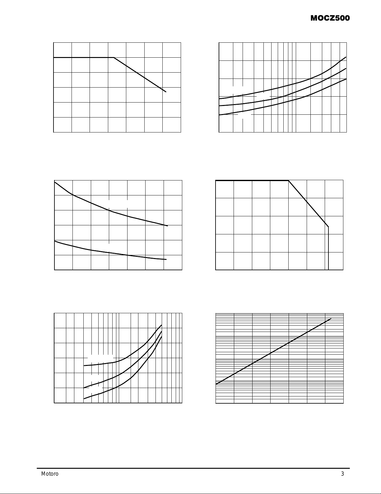
Figure 1. Maximum Allowable Forward LED
Current versus Ambient Temperature
IT = IT Max
14
12
10
, FORWARD TRIGGER CURRENT (mA)
FT
I
8
6
4
2
GUARANTEED
TYPICAL
TA, AMBIENT TEMPERATURE (
1.8
1.6
1.4
TA = –40°C
1.2
, FORWARD VOLTAGE (V)
F
V
1
100806040200–20–40
°
C)
0.8
25°C
85°C
101
IF, FORWARD CURRENT (mA)
Figure 2. LED Forward Voltage versus LED
Forward Current
500
400
300
200
, TERMINAL CURRENT (mA)
T
I
100
100806040200–20–40
°
C)
0
°
TA, AMBIENT TEMPERATURE (
C)
100806040200–20–40
Figure 3. Forward Trigger Current versus
Ambient Temperature
1.4
1.3
1.2
1.1
1
, MAIN TERMINAL VOLTAGE (V)
TM
0.9
V
0.8
0.01 0.1 1
TA = –40°C
25°C
85°C
ITM, MAIN TERMINAL CURRENT (A)
Figure 5. Main T erminal Voltage versus Main
Terminal Current
A)
µ
, LEAKAGE CURRENT (
DRM
I
0.001
Figure 4. RMS ON–State Current versus
Ambient Temperature
10
1
0.1
0.01
100806040200–20–40
TA, AMBIENT TEMPERATURE (°C)
Figure 6. T ypical Leakage Current versus
Ambient Temperature
Motorola Optoelectronics Device Data
3
 Loading...