

Motorola MOC8080 Datasheet
SEMICONDUCTOR TECHNICAL DATA
Order this document
by MOC8080/D
GlobalOptoisolator
The MOC8080 device consists of a gallium arsenide infrared emitting diode
optically coupled to a monolithic silicon photodarlington detector. They are
designed for use in applications requiring high gain at specified input currents.
I
• High Output Collector Current (
• Low, Stable Leakage Current at Elevated Temperature
To order devices that are tested and marked per VDE 0884 requirements, the
•
suffix ”V” must be included at end of part number. VDE 0884 is a test option.
Applications
• Appliances, Measuring Instruments
• General Purpose Switching Circuits
• Programmable Controllers
• Portable Electronics
• Interfacing and coupling systems of different potentials and impedances
• Solid State Relays
MAXIMUM RATINGS
INPUT LED
Reverse Voltage V
Forward Current — Continuous I
LED Power Dissipation @ TA = 25°C
with Negligible Power in Output Detector
Derate above 25°C
OUTPUT DETECTOR
Collector–Emitter Voltage V
Emitter–Collector Voltage V
Collector–Base Voltage V
Collector Current — Continuous I
Detector Power Dissipation @ TA = 25°C
with Negligible Power in Input LED
Derate above 25°C
TOTAL DEVICE
Isolation Surge Voltage
(Peak ac Voltage, 60 Hz, 1 sec Duration)
Total Device Power Dissipation @ TA = 25°C
Derate above 25°C
Ambient Operating Temperature Range
Storage Temperature Range
Soldering Temperature (10 sec, 1/16″ from case) T
1. Isolation surge voltage is an internal device dielectric breakdown rating.
1. For this test, Pins 1 and 2 are common, and Pins 4, 5 and 6 are common.
2. Refer to Quality and Reliability Section in Opto Data Book for information on test conditions.
Preferred devices are Motorola recommended choices for future use and best overall value.
GlobalOptoisolator is a trademark of Motorola, Inc.
(TA = 25°C unless otherwise noted)
Rating
(1)
(2)
)
C
Symbol Value Unit
6 Volts
60 mA
120
1.41
55 Volts
5 Volts
55 Volts
150 mA
150
1.76
7500 Vac(pk)
250
2.94
–55 to +100 °C
–55 to +150 °C
260 °C
mW/°C
mW/°C
mW/°C
(2)
P
CEO
ECO
CBO
P
V
P
T
R
F
D
C
D
ISO
D
T
A
stg
L
mW
mW
mW
[CTR = 500% Min]
Motorola Preferred Device
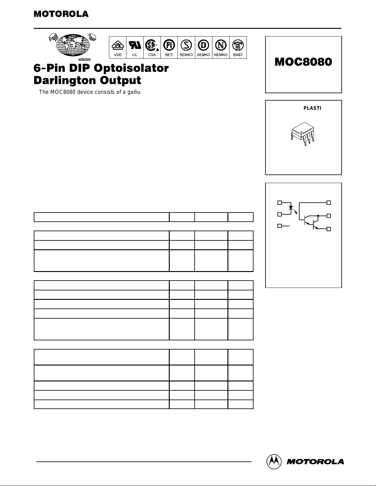
STYLE 1 PLASTIC
6
1
1
STANDARD THRU HOLE
CASE 730A–04
SCHEMATIC
1
2
3
PIN 1. LED ANODE
2. LED CATHODE
3. N.C.
4. EMITTER
5. COLLECTOR
6. BASE
6
5
4
REV 1
Motorola Optoelectronics Device Data
Motorola, Inc. 1995
1
MOC8080
V
10 V, R
100 Ω, I
5 mA
(3)
ELECTRICAL CHARACTERISTICS
Characteristic
INPUT LED
Forward Voltage (IF = 10 mA) TA = 25°C
Reverse Leakage Current (VR = 3 V) I
Capacitance (V = 0 V, f = 1 MHz) C — 18 — pF
OUTPUT DETECTOR
Collector–Emitter Dark Current (V
Collector–Base Dark Current (VCB = 10 V) TA = 25°C
Collector–Emitter Breakdown Voltage (IC = 1 mA) V
Collector–Base Breakdown Voltage (IC = 100 µA) V
Emitter–Collector Breakdown Voltage (IE = 100 µA) V
DC Current Gain (IC = 5 mA, VCE = 5 V) (Typical) h
Collector–Emitter Capacitance (f = 1 MHz, VCE = 5 V) C
Collector–Base Capacitance (f = 1 MHz, VCB = 5 V) C
Emitter–Base Capacitance (f = 1 MHz, VEB = 5 V) C
COUPLED
Output Collector Current (IF = 10 mA, VCE = 5 V) IC (CTR)
Collector–Emitter Saturation Voltage (IC = 1 mA, IF = 1 mA) V
Turn–On Time
Turn–Off Time
Rise Time
Fall Time t
Isolation Voltage (f = 60 Hz, t = 1 sec)
Isolation Resistance (V = 500 V)
Isolation Capacitance (V = 0 V , f = 1 MHz)
1. Always design to the specified minimum/maximum electrical limits (where applicable).
2. Current Transfer Ratio (CTR) = IC/IF x 100%.
3. For test circuit setup and waveforms, refer to Figure 11.
4. For this test, Pins 1 and 2 are common, and Pins 4, 5 and 6 are common.
CC
(TA = 25°C unless otherwise noted)
TA = –55°C
TA = 100°C
= 10 V) TA = 25°C
=
(4)
CE
(4)
(4)
=
L
TA = 100°C
TA = 100°C
=
F
(1)
Symbol Min Typ
V
F
R
I
CEO
I
CBO
(BR)CEO
(BR)CBO
(BR)ECO
FE
CE
CB
EB
(2)
CE(sat)
t
on
t
off
t
r
f
V
ISO
R
ISO
C
ISO
0.8
0.9
0.7
— — 100 µA
—
—
—
—
55 80 — V
55 100 — V
5 7 — V
— 16 k — —
— 3.9 — pF
— 6.3 — pF
— 3.8 — pF
50 (500) 117 (1117) — mA (%)
— 0.6 1 V
— 3.5 —
— 95 —
— 1 —
— 2 —
7500 — — Vac(pk)
11
10
— 0.2 2 pF
(1)
1.15
1.3
1.05
5
5
1
100
— — Ω
Max Unit
1.5
1.7
1.4
100
100
20
—
V
nA
µA
nA
µs
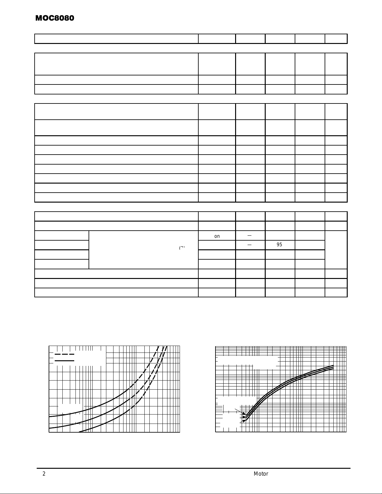
TYPICAL CHARACTERISTICS
2
PULSE ONLY
1.8
1.6
1.4
1.2
, FORWARD VOLTAGE (VOL TS)
F
V
1
1 10 100 1000
PULSE OR DC
TA = –55°C
25°C
100°C
IF, LED FORWARD CURRENT (mA)
10
NORMALIZED TO: IF = 10 mA
1
TA = –55°C THRU
0.1
+25°C
+70°C
+100°C
0.01
, OUTPUT COLLECTOR CURRENT (NORMALIZED)
C
I
TA = 25
°
C
0.5 1 2 5 10 20 50
IF, LED INPUT CURRENT (mA)
Figure 1. LED Forward Voltage versus Forward Current Figure 2. Output Current versus Input Current
2
Motorola Optoelectronics Device Data
 Loading...