

Motorola MMPQ3467 Datasheet
1
Motorola Small–Signal Transistors, FETs and Diodes Device Data
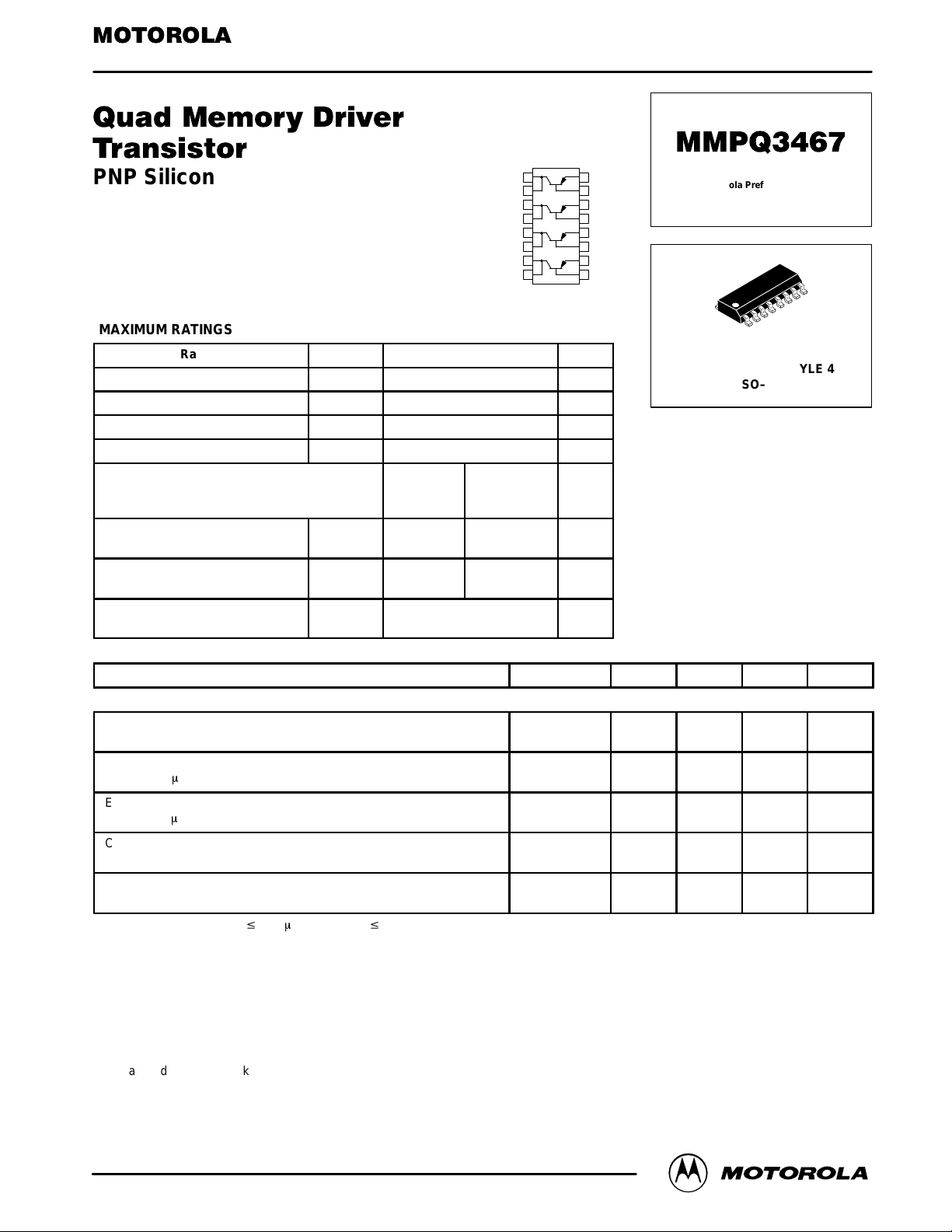
PNP Silicon
MAXIMUM RATINGS
Rating Symbol Value Unit
Collector–Emitter Voltage V
CEO
–40 Vdc
Collector–Base Voltage V
CB
–40 Vdc
Emitter–Base Voltage V
EB
–5.0 Vdc
Collector Current — Continuous I
C
–1.0 Adc
Each
Transistor
Four
Transistors
Equal Power
Power Dissipation @ TA = 25°C
Derate above 25°C
P
D
0.52
4.2
1.2
9.6
Watts
mW/°C
Power Dissipation @ TC = 25°C
Derate above 25°C
P
D
1.0
8.0
2.5
20
Watts
mW/°C
Operating and Storage Junction
Temperature Range
TJ, T
stg
–55 to +150 °C
ELECTRICAL CHARACTERISTICS (T
A
= 25°C unless otherwise noted)
Characteristic
Symbol Min Typ Max Unit
OFF CHARACTERISTICS
Collector–Emitter Breakdown Voltage
(1)
(IC = –10 mAdc, IB = 0)
V
(BR)CEO
–40 — — Vdc
Collector–Base Breakdown Voltage
(IC = –10 mAdc, IE = 0)
V
(BR)CBO
–40 — — Vdc
Emitter–Base Breakdown Voltage
(IE = –10 mAdc, IC = 0)
V
(BR)EBO
–5.0 — — Vdc
Collector Cutoff Current
(VCB = –30 Vdc, IE = 0)
I
CBO
— — –200 nAdc
Emitter Cutoff Current
(VEB = –3.0 Vdc, IC = 0)
I
EBO
— — –200 nAdc
1. Pulse Test: Pulse Width v 300 ms; Duty Cycle v 2.0%.
Thermal Clad is a trademark of the Bergquist Company
Preferred devices are Motorola recommended choices for future use and best overall value.
Order this document
by MMPQ3467/D
SEMICONDUCTOR TECHNICAL DATA
Motorola Preferred Device
CASE 751B–05, STYLE 4
SO–16
1
16
Motorola, Inc. 1996
1
2
3
4
5
6
7
8
10
11
12
13
14
15
16
9
REV 2
MMPQ3467
2
Motorola Small–Signal Transistors, FETs and Diodes Device Data
ELECTRICAL CHARACTERISTICS
(TA = 25°C unless otherwise noted) (Continued)
Characteristic Symbol Min Typ Max Unit
ON CHARACTERISTICS
DC Current Gain
(1)
(IC = –500 mAdc, VCE = –1.0 Vdc)
h
FE
20 — — —
Collector–Emitter Saturation Voltage
(1)
(IC = –500 mAdc, IB = –50 mAdc)
V
CE(sat)
— –0.23 –0.5 Vdc
Base–Emitter Saturation Voltage
(1)
(IC = –500 mAdc, IB = –50 mAdc)
V
BE(sat)
— –0.9 –1.2 Vdc
DYNAMIC CHARACTERISTICS
Current–Gain — Bandwidth Product
(IC = –50 mAdc, VCE = –10 Vdc, f = 100 MHz)
f
T
— 190 — MHz
Output Capacitance
(VCB = –10 Vdc, IE = 0, f = 1.0 MHz)
C
ob
— 10 — pF
Input Capacitance
(VEB = –0.5 Vdc, IC = 0, f = 1.0 MHz)
C
ib
— 55 — pF
SWITCHING CHARACTERISTICS
Turn–On Time
(IC = –500 mAdc, IB1 = –50 mAdc)
t
on
— 20 — ns
Turn–Off Time
(IC = –500 mAdc, IB1 = IB2 = –50 mAdc)
t
off
— 60 — ns
1. Pulse Test: Pulse Width v 300 ms; Duty Cycle v 2.0%.
 Loading...