

Motorola MMGA20VT1, MMGA5V6T1 Datasheet
1
MOTOROLA
MMQA5V6T1 MMQA20VT1
Transient Voltage Suppressor
for ESD Protection
This quad monolithic silicon voltage suppressor is designed for applications
requiring transient overvoltage protection capability. It is intended for use in
voltage and ESD sensitive equipment such as computers, printers, business
machines, communication systems, medical equipment, and other applications. Its quad junction common anode design protects four separate lines
using only one package. These devices are ideal for situations where board
space is at a premium.
Specification Features:
• SC-59 Package Allows Four Separate Unidirectional Configurations
• Peak Power — 24 Watts @ 1.0 ms (Unidirectional), per Figure 7 Waveform
• Maximum Clamping Voltage @ Peak Pulse Current
• Low Leakage < 2.0 µA
• ESD Rating of Class N (exceeding 16 kV) per the Human Body Model
Mechanical Characteristics:
• Void Free, Transfer-Molded, Thermosetting Plastic Case
• Corrosion Resistant Finish, Easily Solderable
• Package Designed for Optimal Automated Board Assembly
• Small Package Size for High Density Applications
• Available in 8 mm Tape and Reel
Use the Device Number to order the 7 inch/3,000 unit reel. Replace
with “T3” in the Device Number to order the 13 inch/10,000 unit reel.
THERMAL CHARACTERISTICS
(TA = 25°C unless otherwise noted)
Characteristic
Symbol Value Unit
Peak Power Dissipation @ 1.0 ms (1)
@ TA ≤ 25°C
P
pk
24 Watts
Total Power Dissipation on FR-5 Board (2) @ TA = 25°C
Derate above 25°C
°PD° °225
1.8
°mW°
mW/°C
Thermal Resistance Junction to Ambient R
θJA
556 °C/W
Total Power Dissipation on Alumina Substrate (3) @ TA = 25°C
Derate above 25°C
°PD° °300
2.4
°mW
mW/°C
Thermal Resistance Junction to Ambient R
θJA
417 °C/W
Junction and Storage Temperature Range T
J
T
stg
°– 55 to +150° °C
Lead Solder Temperature — Maximum (10 Second Duration) T
L
260 °C
1. Non-repetitive current pulse per Figure 7 and derate above TA = 25°C per Figure 8.
2. FR-5 = 1.0 x 0.75 x 0.62 in.
3. Alumina = 0.4 x 0.3 x 0.024 in., 99.5% alumina
4. Other voltages are available
Thermal Clad is a trademark of the Bergquist Company
Preferred devices are Motorola recommended choices for future use and best overall value.
SEMICONDUCTOR TECHNICAL DATA
Order this document
by MMQA5V6T1/D
Motorola, Inc. 1996
Rev 3
SC-59 QUAD
TRANSIENT VOLTAGE
SUPPRESSOR
5.6 VOLTS (4)
24 WATTS PEAK POWER
CASE 318F-01
STYLE 1
SC-59 PLASTIC
4 5
6
Motorola Preferred Devices
PIN 1. CATHODE
2. ANODE
3. CATHODE
4. CATHODE
5. ANODE
6. CATHODE
1
2
3
1
2
3
4
5
6

MOTOROLA
2
MMQA5V6T1 MMQA20VT1
ELECTRICAL CHARACTERISTICS (T
A
= 25°C unless otherwise noted)
UNIDIRECTIONAL (Circuit tied to pins 1, 2, and 5; Pins 2, 3, and 5; Pins 2, 4, and 5; or Pins 2, 5, and 6) (V
F
= 0.9 V Max @ IF = 10 mA)
Breakdown Voltage
Max Reverse
Leakage Current
Max Zener Impedance (5)
Max
Reverse
Max Reverse
Voltage @
Maximum
VZT(3)
(V)
@ I
ZT
IR @ VR
ZZT @ IZT
Surge
Current
I
RSM(4)
I
RSM
(4)
(Clamping
Voltage)
Temperature
Coefficient of
V
Z
Min Nom Max
(mA)
1
(µA) (V)
(Ω) (mA)
I
RSM(4)
(A)
V
RSM
(V)
(mV/°C)
5.32 5.6 5.88 1.0 2.0 3.0 400 3.0 8.0 1.26
19 20 21 1.0 0.1 15 125 0.84 28.6 20.07
(3) VZ measured at pulse test current IT at an ambient temperature of 25°C.
(4) Surge current waveform per Figure 5 and derate per Figure 6.
(5) ZZT is measured by dividing the AC voltage drop across the device by the AC current supplied. The specfied limits are I
Z(AC)
= 0.1 I
Z(DC)
, with AC frequency = 1 kHz.
Typical Characteristics
– 50 50 100 150
8
7
6
5
4
V ,
Z
BREAKDOWN VOLTAGE (VOLTS)
23
17
TA, AMBIENT TEMPERATURE (
°
C)
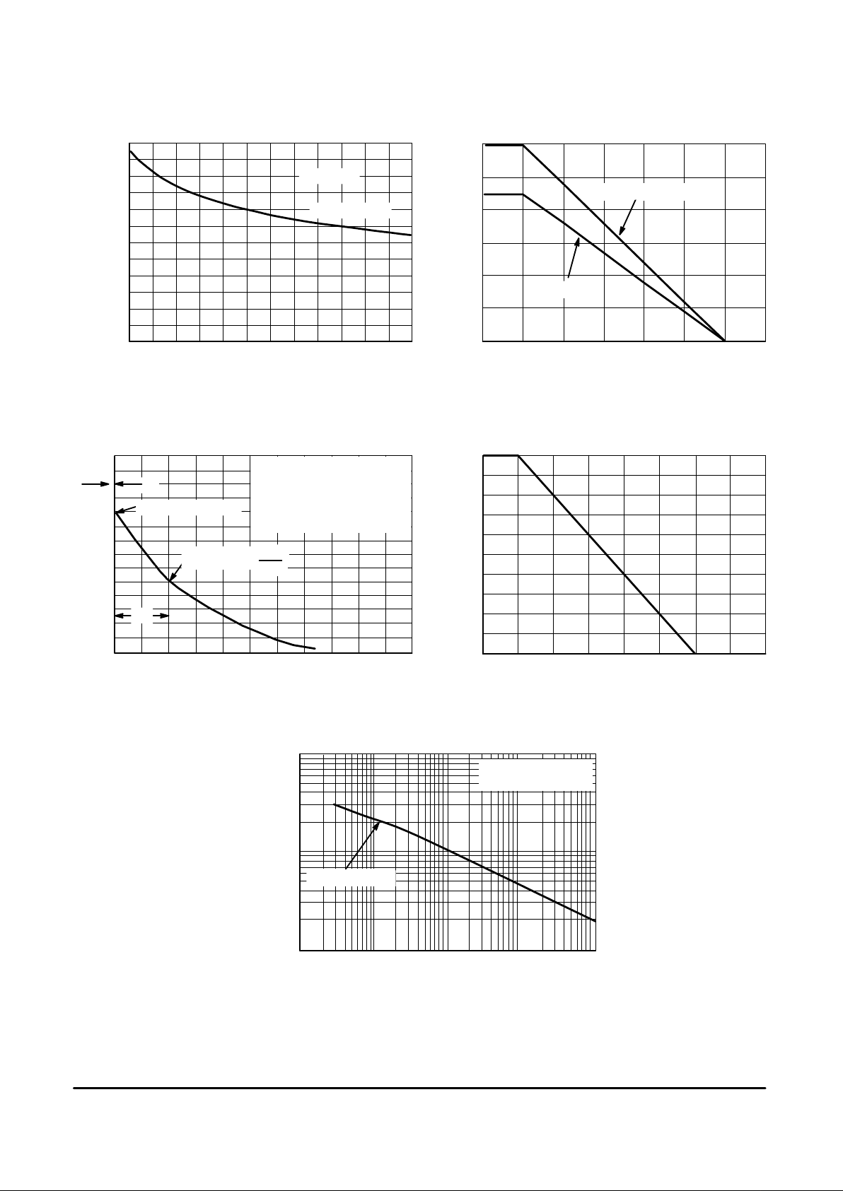
Figure 1. Typical Breakdown Voltage
versus Temperature
Figure 2. Typical Breakdown Voltage
versus Temperature
0 2 4 6 8 10 14 16
70
60
50
40
30
20
0
C, CAPACITANCE (pF)
0 – 40 25 150
TA, AMBIENT TEMPERATURE (
°
C)
REVERSE VOLTAGE (V)
VZ @ I
T
MMQA5V6T1
22
21
20
19
18
MMQA20VT1
10000
1000
100
TA, AMBIENT TEMPERATURE (
°
C)
I
R,
REVERSE LEAKAGE CURRENT (nA)
– 50 50 100 1500
Figure 3. Typical Leakage Current
versus Temperature
Figure 4. Typical Capacitance versus
Reverse Voltage
10
12
MMQA20VT1
UNIDIRECTIONAL
V ,
Z
BREAKDOWN VOLTAGE (VOLTS)
0
UNIDIRECTIONAL
3
MOTOROLA
MMQA5V6T1 MMQA20VT1
Typical Characteristics
0 1 1.5 3
300
Figure 5. Typical Capacitance versus
Reverse Voltage
0 25 50 75 100 125 150 175
300
250
200
150
100
50
0
Figure 6. Steady State Power Derating Curve
P
D
, POWER DISSIPATION (mW)
0.5
REVERSE VOLTAGE (V)
TA, AMBIENT TEMPERATURE (
°
C)
FR-5 BOARD
ALUMINA SUBSTRATE
C, CAPACITANCE (pF)
2 2.5
275
250
225
200
175
150
125
100
75
50
25
0
UNIDIRECTIONAL
MMQA5V6T1
VALUE (%)
100
50
0
0 1 2 3 4
t, TIME (ms)
Figure 7. Pulse Waveform
t
r
t
P
100
90
80
70
60
50
40
30
20
10
0
0 25 50 75 100 125 150 175 200
TA, AMBIENT TEMPERATURE (
°
C)
Figure 8. Pulse Derating Curve
PEAK PULSE DERATING IN % OF PEAK POWER
OR CURRENT @ T
A
= 25
C
°
Figure 9. Maximum Non-repetitive Surge
Power, Ppk versus PW
Ppk PEAK SURGE POWER (W)
0.1 1.0 10 100 1000
1.0
10
100
Power is defined as V
RSM
x IZ(pk) where V
RSM
is the clamping voltage at IZ(pk).
PW, PULSE WIDTH (ms)
PULSE WIDTH (tP) IS DEFINED
AS THAT POINT WHERE THE
PEAK CURRENT DECAYS TO 50%
OF I
RSM
.
tr
≤
10 µs
HALF VALUE—
I
RSM
2
PEAK VALUE—I
RSM
UNIDIRECTIONAL
RECTANGULAR
WAVEFORM, TA = 25
°
C
 Loading...