

MOTOROLA MMG05N60D, MMG05N60DT1, MMG05N60DT3 Datasheet
1
Motorola IGBT Device Data
N–Channel Enhancement–Mode Silicon Gate
This IGBT contains a built–in free wheeling diode and a gate
protection zener diodes. Fast switching characteristics result in
efficient operation at higher frequencies. This device is ideally
suited for high frequency electronic ballasts.
• Built–In Free Wheeling Diode
• Built–In Gate Protection Zener Diodes
• Industry Standard Package (SOT223)
• High Speed E
off
: Typical 6.5 mJ @ IC = 0.3 A; TC = 125°C and
dV/dt = 1000 V/ms
• Robust High Voltage Termination
• Robust Turn–Off SOA
MAXIMUM RATINGS
(TJ = 25°C unless otherwise noted)
Parameters Symbol Value Unit
Collector–Emitter Voltage V
CES
600 Vdc
Collector–Gate Voltage (RGE = 1.0 MΩ) V
CGR
600 Vdc
Gate–Emitter Voltage — Continuous V
CGR
±15 Vdc
Collector Current — Continuous @ TC = 25°C
Collector Current — Continuous @ TC = 90°C
Collector Current — Repetitive Pulsed Current (1)
I
C25
I
C90
I
CM
0.5
0.3
2.0
Adc
Total Device Dissipation @ TC = 25°C P
D
1.0 Watt
Operating and Storage Junction Temperature Range TJ, T
stg
–55 to 150 °C
Thermal Resistance — Junction to Case – IGBT
Thermal Resistance — Junction to Ambient
R
θJC
R
θJA
30
150
°C/W
Maximum Lead Temperature for Soldering Purposes, 1/8″ from case for 5 seconds T
L
260 °C
UNCLAMPED DRAIN–TO–SOURCE AVALANCHE CHARACTERISTICS (T
C
≤ 150°C)
Single Pulse Drain–to–Source Avalanche
Energy – Starting @ TC = 25°C
Energy – Starting @ TC = 125°C
VCE = 100 V , VGE = 15 V, Peak IL = 2.0 A, L = 3.0 mH, RG = 25
W
E
AS
125
40
mJ
(1) Pulse width is limited by maximum junction temperature repetitive rating.
Designer’s Data for “Worst Case” Conditions— The Designer’s Data Sheet permits the design of most circuits entirely from the information presented. SOA Limit
curves — representing boundaries on device characteristics — are given to facilitate “worst case” design.
Designer’s is a trademark of Motorola, Inc.
REV 2
Order this document
by MMG05N60D/D
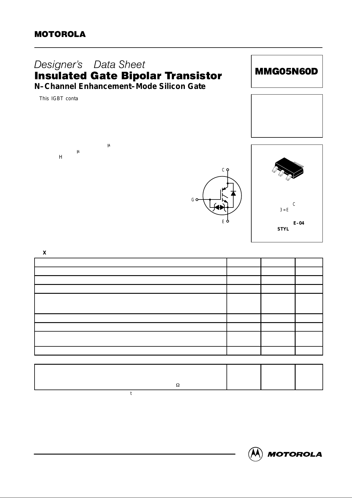
SEMICONDUCTOR TECHNICAL DATA
IGBT
0.5 A @ 25°C
600 V
CASE 318E–04
STYLE 13
TO–261A
1
2
3
4
1 = G
2 = 4 = C
3 = E
C
E
G
Motorola, Inc. 1998
MMG05N60D
2
Motorola IGBT Device Data
ELECTRICAL CHARACTERISTICS
(T
J
= 25°C unless otherwise noted)
Characteristic
Symbol Min Typ Max Unit
OFF CHARACTERISTICS
Collector–to–Emitter Breakdown Voltage
(VGE = 0 Vdc, IC = 250 µAdc)
T emperature Coef ficient (Positive)
V
(BR)CES
600
—
680
0.7
—
—
Vdc
V/°C
Zero Gate Voltage Collector Current
(VCE = 600 Vdc, VGE = 0 Vdc, TC = 25°C)
(VCE = 600 Vdc, VGE = 0 Vdc, TC = 125°C)
I
CES
I
CES
—
—
0.1
5.0
5.0
50
µAdc
Gate–Body Leakage Current (VGE = ±15 Vdc, VCE = 0 Vdc) I
GES
— 10 100
m
Adc
ON CHARACTERISTICS
Collector–to–Emitter On–State Voltage
(VGE = 15 Vdc, IC = 0.3 Adc, TC = 25°C)
(VGE = 15 Vdc, IC = 0.3 Adc, TC = 125°C)
V
CE(on)
—
—
1.6
1.5
2.0
—
Vdc
Gate Threshold Voltage
(VCE = VGE, IC = 250 mAdc)
Threshold Temperature Coefficient (Negative)
V
GE(th)
3.5
—
—
6.0
6.0
—
Vdc
mV/°C
Forward Transconductance (VCE = 10 Vdc, IC = 0.5 Adc) g
fe
0.3 0.42 — Mhos
DYNAMIC CHARACTERISTICS
Input Capacitance
C
ies
— 75 100 pF
Output Capacitance
(VCE = 20 Vdc, VGE = 0 Vdc,
f = 1.0 MHz
)
C
oes
— 11 20
Transfer Capacitance
f = 1.0 MHz)
C
res
— 1.6 5.0
DIODE CHARACTERISTICS
Diode Forward Voltage Drop
(IEC = 0.3 Adc, TC = 25°C)
(IEC = 0.3 Adc, TC = 125°C)
(IEC = 0.1 Adc, TC = 25°C)
(IEC = 0.1 Adc, TC = 125°C)
V
FEC
—
—
—
—
5.0
5.2
2.3
2.3
6.0
—
3.0
—
Vdc
Reverse Recovery Time @ TC = 25°C
IF = 0.4 Adc, VR = 300 Vdc, dIF/dt = 10 A/ms
t
rr
— 150 —
ns
Reverse Recovery Stored Charge
IF = 0.4 Adc, VR = 300 Vdc, dIF/dt = 10 A/ms
Q
RR
— 35 —
m
C
SWITCHING CHARACTERISTICS (1)
Turn–Off Delay Time
(VCC = 300 Vdc, IC = 0.4 Adc,
t
d(off)
— 28 — ns
Fall Time
VGE = 15 Vdc, L = 3.0 mH, RG = 25 Ω,
T
= 25°C, dV/dt = 1000 V/ms
)
t
f
— 150 —
Turn–Off Switching Loss
T
C
=
25 C, dV/dt = 1000 V/ms)
Energy losses include “tail”
E
off
— 3.25 4.25
m
J
Turn–Off Delay Time
(VCC = 300 Vdc, IC = 0.4 Adc,
t
d(off)
— 21 — ns
Fall Time
VGE = 15 Vdc, L = 3.0 mH, RG = 25 Ω,
T
= 125°C, dV/dt = 1000 V/ms
)
t
f
— 280 —
Turn–Off Switching Loss
T
C
=
125 C, dV/dt = 1000 V/ms)
Energy losses include “tail”
E
off
— 8.0 10
m
J
Gate Charge (VCC = 300 Vdc, IC = 0.3 Adc,
VGE = 15 Vdc)
Q
T
— 6.4 — nC
(1) Pulse Test: Pulse Width ≤ 300 µs, Duty Cycle ≤ 2%.
 Loading...