

Motorola MMFT960T1 Datasheet
SEMICONDUCTOR TECHNICAL DATA
Order this document
by MMFT960T1/D
N–Channel Enhancement–Mode
Silicon Gate TMOS
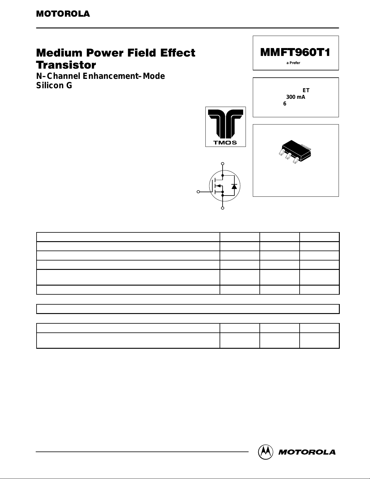
SOT–223 for Surface Mount
This TMOS medium power field effect transistor is designed for
high speed, low loss power switching applications such as
switching regulators, dc–dc converters, solenoid and relay drivers.
The device is housed in the SOT–223 package which is designed
for medium power surface mount applications.
• Silicon Gate for Fast Switching Speeds
• R
DS(on)
= 1.7 Ohm Max
• Low Drive Requirement
• The SOT–223 Package can be soldered using wave or reflow.
The formed leads absorb thermal stress during soldering
eliminating the possibility of damage to the die.
• Available in 12 mm Tape and Reel
Use MMFT960T1 to order the 7 inch/1000 unit reel
Use MMFT960T3 to order the 13 inch/4000 unit reel
MAXIMUM RATINGS
Drain–to–Source Voltage V
Gate–to–Source Voltage — Non–Repetitive V
Drain Current I
Total Power Dissipation @ TA = 25°C
Derate above 25°C
Operating and Storage Temperature Range TJ, T
(TC = 25°C unless otherwise noted)
Rating Symbol Value Unit
(1)
1
GATE
DEVICE MARKING
FT960
THERMAL CHARACTERISTICS
Thermal Resistance — Junction–to–Ambient R
Maximum Temperature for Soldering Purposes
Time in Solder Bath
1. Device mounted on a FR–4 glass epoxy printed circuit board using minimum recommended footprint.
2,4 DRAIN
3 SOURCE
DS
GS
D
P
D
θJA
T
L
stg
Motorola Preferred Device
MEDIUM POWER
TMOS FET
300 mA
60 VOLTS
R
CASE 318E–04, STYLE 3
–65 to 150 °C
= 1.7 OHM MAX
DS(on)
1
2
3
TO–261AA
60 Volts
±30 Volts
300 mAdc
0.8
6.4
156 °C/W
260
10
4
Watts
mW/°C
°C
Sec
TMOS is a registered trademark of Motorola, Inc.
Thermal Clad is a trademark of the Bergquist Company
Preferred devices are Motorola recommended choices for future use and best overall value.
REV 3
Motorola Small–Signal Transistors, FETs and Diodes Device Data
Motorola, Inc. 1997
1
MMFT960T1
)
f = 1.0 MHz)
)
V
DS
V)
ELECTRICAL CHARACTERISTICS
Characteristic Symbol Min Typ Max Unit
(TA = 25°C unless otherwise noted)
OFF CHARACTERISTICS
Drain–to–Source Breakdown V oltage
(VGS = 0, ID = 10 µA)
Zero Gate Voltage Drain Current
(VDS = 60 V, VGS = 0)
Gate–Body Leakage Current
(VGS = 15 Vdc, VDS = 0)
ON CHARACTERISTICS
Gate Threshold Voltage
(VDS = VGS, ID = 1.0 mAdc)
Static Drain–to–Source On–Resistance
(VGS = 10 Vdc, ID = 1.0 A)
Drain–to–Source On–Voltage
(VGS = 10 V, ID = 0.5 A)
(VGS = 10 V, ID = 1.0 A)
Forward Transconductance
(VDS = 25 V, ID = 0.5 A)
(1)
DYNAMIC CHARACTERISTICS
Input Capacitance
Output Capacitance
Transfer Capacitance
Total Gate Charge
Gate–Source Charge
Gate–Drain Charge
1. Pulse Test: Pulse Width ≤ 300 µs, Duty Cycle ≤2.0%.
(VDS = 25 V, VGS = 0,
f = 1.0 MHz
(VGS = 10 V, ID = 1.0 A,
V
= 48 V
= 48
V
(BR)DSS
I
DSS
I
GSS
V
GS(th)
R
DS(on)
V
DS(on)
g
fs
C
iss
C
oss
C
rss
Q
Q
gs
Q
gd
60 — — Vdc
— — 10 µAdc
— — 50 nAdc
1.0 — 3.5 Vdc
— — 1.7 Ohms
—
—
— 600 — mmhos
— 65 —
— 33 —
— 7.0 —
g
— 3.2 —
— 1.2 —
— 2.0 —
—
—
0.8
1.7
Vdc
pF
nC
5
4
3
2
, DRAIN CURRENT (AMPS)
D
I
1
0
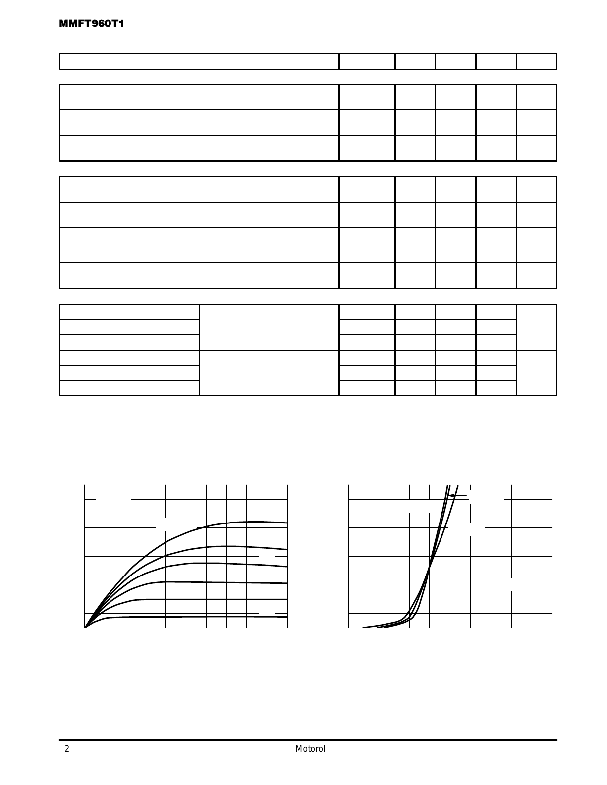
TYPICAL ELECTRICAL CHARACTERISTICS
1
TJ = 25°C
VGS = 10 V
VDS, DRAIN–TO–SOURCE VOL TAGE (VOLTS)
8 V
7 V
6 V
5 V
4 V
0.8
0.6
0.4
, DRAIN CURRENT (AMPS)
D
I
0.2
1086420
0
TJ = –55°C
VGS, GATE–T O–SOURCE VOLTAGE (VOLTS)
Figure 1. On–Region Characteristics Figure 2. Transfer Characteristics
TJ = 25°C
TJ = 125°C
VDS = 10 V
1086420
2
Motorola Small–Signal Transistors, FETs and Diodes Device Data
 Loading...