

Motorola MMFT3055EL Datasheet
1
Motorola TMOS Power MOSFET Transistor Device Data
N–Channel Enhancement Mode
Silicon Gate TMOS E–FET
t
SOT–223 for Surface Mount
This advanced E–FET is a TMOS power MOSFET designed to
withstand high energy in the avalanche and commutation modes.
This device is also designed with a low threshold voltage so it is
fully enhanced with 5 Volts. This new energy efficient device also
offers a drain–to–source diode with a fast recovery time. Designed
for low voltage, h igh s peed switching applications i n power
supplies, converters and PWM motor controls, these devices are
particularly well suited for bridge circuits where diode speed and
commutating safe operating areas are critical and offer additional
safety margin against unexpected voltage transients. The device is
housed in the SOT–223 package which is designed for medium
power surface mount applications.
• Silicon Gate for Fast Switching Speeds
• Low Drive Requirement to Interface Power Loads to Logic
Level ICs, V
GS(th)
= 2 Volts Max
• Low R
DS(on)
— 0.18 Ω max
• The SOT–223 Package can be Soldered Using Wave or Re-
flow. The Formed Leads Absorb Thermal Stress During Soldering, Eliminating the Possibility of Damage to the Die
• Available in 12 mm Tape and Reel
Use MMFT3055ELT1 to order the 7 inch/1000 unit reel.
Use MMFT3055ELT3 to order the 13 inch/4000 unit reel.
MAXIMUM RATINGS
(TA = 25°C unless otherwise noted)
Rating
Symbol Value Unit
Drain–to–Source Voltage V
DS
60
Gate–to–Source Voltage — Continuous V
GS
±15
Vdc
Drain Current — Continuous
Drain Current — Pulsed
I
D
I
DM
1.5
6
Adc
Total Power Dissipation @ TA = 25°C
Derate above 25°C
P
D
(1)
0.8
6.4
Watts
mW/°C
Operating and Storage Temperature Range TJ, T
stg
–65 to 150 °C
Single Pulse Drain–to–Source Avalanche Energy — Starting TJ = 25°C
(VDD = 25 V, VGS = 5 V, Peak IL= 1.5 A, L = 0.2 mH, RG = 25 Ω)
E
AS
178 mJ
DEVICE MARKING
3055L
THERMAL CHARACTERISTICS
Thermal Resistance — Junction–to–Ambient (surface mounted) R
θJA
156 °C/W
Maximum Temperature for Soldering Purposes,
Time in Solder Bath
T
L
260
5
°C
Sec
(1) Power rating when mounted on FR–4 glass epoxy printed circuit board using recommended footprint.
TMOS is a registered trademark of Motorola, Inc.
E–FET is a trademark of Motorola, Inc.
Thermal Clad is a trademark of the Bergquist Company
Preferred devices are Motorola recommended choices for future use and best overall value.
REV 3
Order this document
by MMFT3055EL/D
SEMICONDUCTOR TECHNICAL DATA
Motorola, Inc. 1995
MEDIUM POWER
LOGIC LEVEL TMOS FET
1.5 AMP
60 VOLTS
R
DS(on)
= 0.18 OHM
Motorola Preferred Device
CASE 318E–04, STYLE 3
TO–261AA
D
S
G
2,4
3
1
1
2
3
4
MMFT3055EL
2
Motorola TMOS Power MOSFET Transistor Device Data
ELECTRICAL CHARACTERISTICS
(TA = 25°C unless otherwise noted)
Characteristic
Symbol Min Typ Max Unit
OFF CHARACTERISTICS
Drain–to–Source Breakdown Voltage, (VGS = 0, ID = 250 µA) V
(BR)DSS
60 — — Vdc
Zero Gate Voltage Drain Current, (VDS = 60 V, VGS = 0) I
DSS
— — 10 µAdc
Gate–Body Leakage Current, (VGS = 15 V, VDS = 0) I
GSS
— — 100 nAdc
ON CHARACTERISTICS
Gate Threshold Voltage, (VDS = VGS, ID = 1.0 mA) V
GS(th)
1 — 2 Vdc
Static Drain–to–Source On–Resistance, (VGS = 5 V, ID = 0.75 A) R
DS(on)
— — 0.18 Ohms
Drain–to–Source On–Voltage, (VGS = 5 V, ID = 1.5 A) V
DS(on)
— — 0.36 Vdc
Forward Transconductance, (VDS = 15 V, ID = 0.75 A) g
FS
— 2.1 — mhos
DYNAMIC CHARACTERISTICS
Input Capacitance
C
iss
— 500 —
Output Capacitance
(VDS = 25 V,
VGS = 0,
C
oss
— 175 —
Reverse Transfer Capacitance
f = 1 MHz)
C
rss
— 40 —
SWITCHING CHARACTERISTICS
Turn–On Delay Time
t
d(on)
— 20 —
Rise Time
t
r
— 95 —
Turn–Off Delay Time
VGS = 5 V, RG = 50 ohms,
RGS = 25 ohms)
t
d(off)
— 38 —
ns
Fall Time
GS
= 25 ohms)
t
f
— 50 —
Total Gate Charge
Q
g
— 7 15
Gate–Source Charge
(VDS = 48 V, ID = 1.5 A,
VGS = 5 Vdc)
Q
gs
— 1.3 —
Gate–Drain Charge
See Figures 15 and 16
Q
gd
— 6.3 —
SOURCE DRAIN DIODE CHARACTERISTICS
(1)
Forward On–Voltage IS = 1.5 A, VGS = 0 V
SD
— 1.0 — Vdc
Forward Turn–On Time
t
on
Limited by stray inductance
Reverse Recovery Time
dlS/dt = 400 A/µs,
VR = 30 V
t
rr
— 55 —
ns
(1) Pulse Test: Pulse Width ≤ 300 µs, Duty Cycle ≤ 2%
(VDD= 25 V, ID = 6 A
IS = 1.5 A, VGS =
0,
pF
nC
MMFT3055EL
3
Motorola TMOS Power MOSFET Transistor Device Data
R
DS(on)
, DRAIN–TO–SOURCE RESISTANCE (OHMS)R
DS(on)
, DRAIN–TO–SOURCE RESISTANCE (OHMS)
R
DS(on)
, DRAIN–TO–SOURCE RESISTANCE (OHMS)
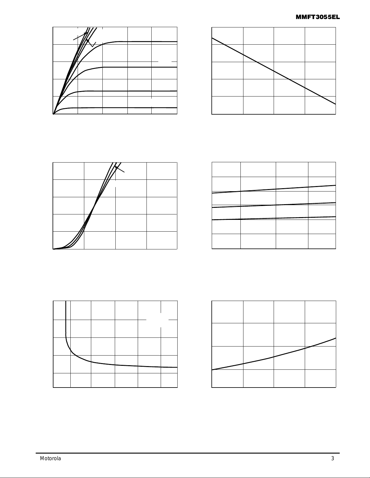
Figure 1. On Region Characteristics
D
I , DRAIN CURRENT (AMPS)
0 1.0 2.0 3.0 4.0 5.0
VDS, DRAIN–TO–SOURCE VOLTAGE (VOLTS)
TJ = 25°C
6.0 V
5.5 V
4.5 V
5.0 V
4.0 V
3.5 V
3.0 V
VGS = 2.5 V
GS(TH)
V , GATE THRESHOLD VOLTAGE
Figure 2. Gate–Threshold Voltage Variation
With Temperature
1.2
1.1
1.0
0.9
0.8
0.7
–50 0 50 100 150
TJ, JUNCTION TEMP (
°
C)
(NORMALIZED)
Figure 3. Transfer Characteristics
D
I , DRAIN CURRENT (AMPS)
0 2.0 4.0 6.0 7.0
VGS, GATE–TO–SOURCE VOLTAGE (VOLTS)
TJ = –55°C
25
°
C
Figure 4. On–Resistance versus Drain Current
0 1.0 2.0 3.0 4.0
ID, DRAIN CURRENT (AMPS)
Figure 5. On–Resistance versus
Gate–to–Source Voltage
2.0 3.0 4.0 5.0 6.0 7.0
VGS, GATE–TO–SOURCE VOLTAGE (VOLTS)
TJ = 25°C
ID = 1.5 A
8.0
0.1
0.2
0.3
0.4
0.5
0
Figure 6. On–Resistance versus
Junction Temperature
0.4
0.3
0.2
0.1
0
–50 0 50 100 150
TJ, JUNCTION TEMP (
°
C)
VGS = 5 V
ID = 1.5 A
0
0.05
0.10
0.15
0.20
0.25
0.30
TJ = 100
°
C
55
°
C
25
°
C
VDS = 8 V
VGS = 5 V
VDS = V
GS
ID = 1.0 mA
10
8.0
6.0
4.0
2.0
0
10
8.0
6.0
4.0
2.0
0
100°C
 Loading...