

Motorola MMFT108T1 Datasheet
SEMICONDUCTOR TECHNICAL DATA
Order this document
by MMFT108T1/D
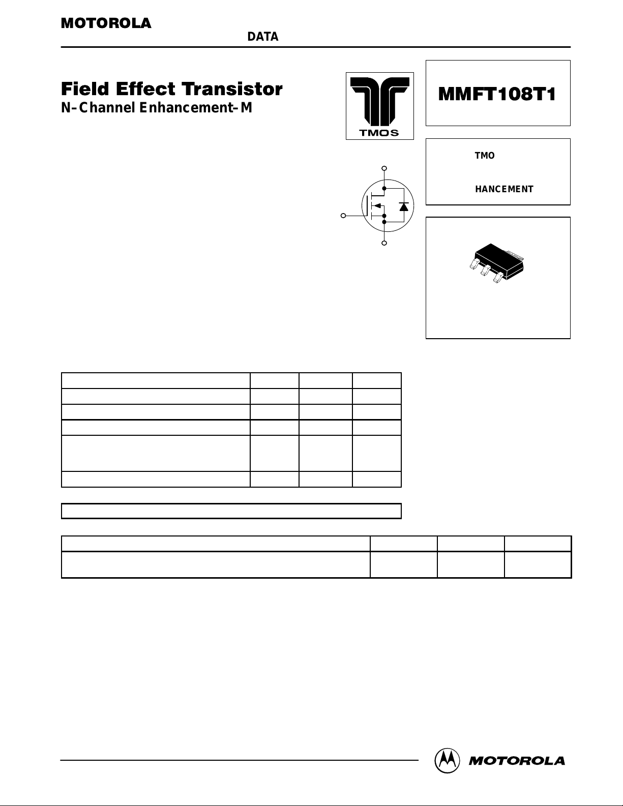
N–Channel Enhancement–Mode
Logic Level SOT–223
2, 4 DRAIN
1
GATE
3 SOURCE
MAXIMUM RATINGS
Rating Symbol Value Unit
Drain–to–Source Voltage V
Gate–to–Source Voltage — Continuous V
Drain Current — Continuous I
Total Power Dissipation
@ TA = 25°C
Derate above 25°C
Operating and Storage Temperature Range TJ, T
DSS
GS
D
P
D
stg
DEVICE MARKING
MT108
THERMAL CHARACTERISTICS
Thermal Resistance — Junction–to–Ambient
Maximum Temperature for Soldering Purposes
Maximum Time in Solder Bath
1. Device mounted on FR4 glass epoxy printed circuit using minimum recommended foot print.
(1)
200 Volts
±20 Volts
250 mAdc
0.8
6.4
–65 to +150 °C
Watts
mW/°C
TMOS FET
TRANSISTOR
N–CHANNEL —
ENHANCEMENT
4
1
2
3
CASE 318E–04, STYLE 3
SOT–223 (TO–261AA)
R
θJA
T
L
156 °C/W
260
10
°C
Sec
TMOS is a registered trademark of Motorola, Inc.
Motorola Small–Signal Transistors, FETs and Diodes Device Data
Motorola, Inc. 1997
1
MMFT108T1
)
f = 1.0 MHz)
ELECTRICAL CHARACTERISTICS
Characteristic Symbol Min Typ Max Unit
(TA = 25°C unless otherwise noted)
OFF CHARACTERISTICS
Drain–to–Source Breakdown V oltage
(VGS = 0, ID = 10 mA)
Zero Gate Voltage Drain Current
(VDS = 130 V, VGS = 0)
Gate–Body Leakage Current — Reverse
(VGS = 15 Vdc, VDS = 0)
ON CHARACTERISTICS
Gate Threshold Voltage
(ID = 1.0 mAdc, VDS = VGS)
Static Drain–to–Source On–Resistance
(VGS = 2.0 Vdc, ID = 50 mA)
(VGS = 2.8 Vdc, ID = 100 mA)
Drain Cutoff Current
(VGS = 0.2 V, VDS = 70 V)
(2)
DYNAMIC CHARACTERISTICS
Input Capacitance
Output Capacitance
Transfer Capacitance
(VDS = 25 V, VGS = 0,
f = 1.0 MHz
SWITCHING CHARACTERISTICS
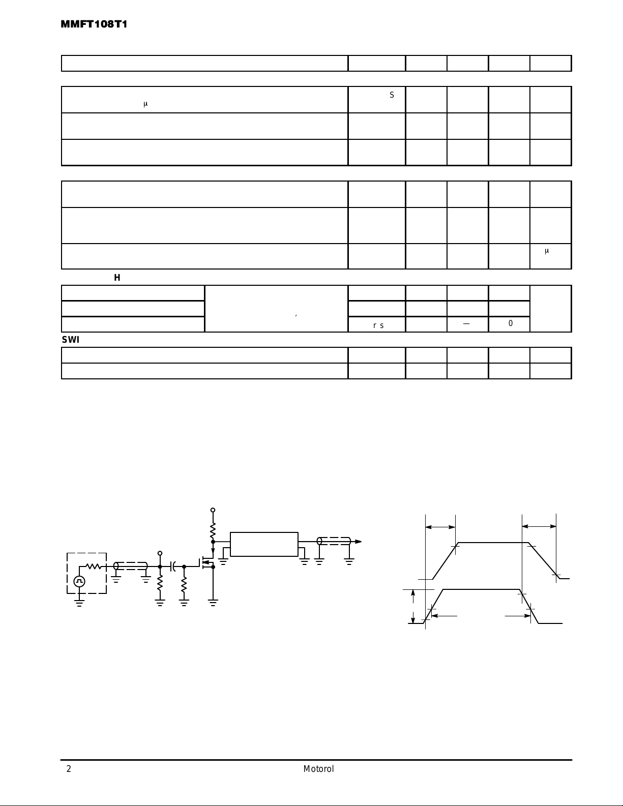
Turn–On Time (See Figure 1) t
Turn–Off T ime (See Figure 1) t
2. Pulse Test: Pulse Width ≤ 300 µs, Duty Cycle =2.0%.
V
(BR)DSS
I
DSS
I
GSS
V
GS(th)
r
DS(on)
I
DSX
C
iss
C
oss
C
rss
on
off
200 — —
— — 30
— — 10
0.5 — 1.5
—
—
— — 25
— — 150
— — 30
— — 10
— — 15 ns
— — 15 ns
—
—
10
8.0
nAdc
nAdc
Ohms
Vdc
Vdc
m
pF
A
PULSE GENERAT OR
50
+25 V
23
V
in
50
40 pF
1.0 M
50
Ω
Figure 1. Switching Test Circuit
RESISTIVE SWITCHING
TO SAMPLING SCOPE
50
20 dB
ATTENUATOR
Ω
INPUT
V
OUTPUT
INVERTED
INPUT
out
t
on
90% 90%
V
out
90%
10 V
V
in
50%
10%
PULSE
WIDTH
50%
Figure 2. Switching Waveforms
t
off
10%
2
Motorola Small–Signal Transistors, FETs and Diodes Device Data
 Loading...