

Motorola MMDJ3P03BJT Datasheet
Î
Î
Î
Î
Î
Î
SEMICONDUCTOR TECHNICAL DATA
Order this document
by MMDJ3P03BJT/D
Motorola Preferred Device
SO–8 for Surface Mount Applications
• Collector –Emitter Sustaining Voltage — V
CEO(sus)
= 30 Vdc (Min) @ IC = 10 mAdc
• High DC Current Gain — h
FE
= 140 (Min) @ IC = 1.2 Adc
= 125 (Min) @ IC = 3.0 Adc
• Low Collector –Emitter Saturation Voltage — V
CE(sat)
= 0.24 Vdc (Max) @ IC = 1.2 Adc
= 0.60 Vdc (Max) @ IC = 5.0 Adc
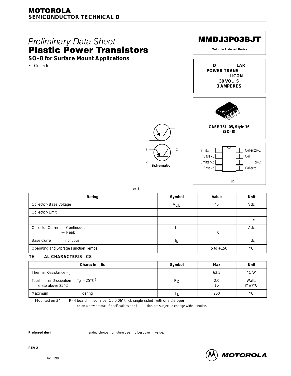
• Miniature SO–8 Surface Mount Package – Saves Board Space
E
B
E
B
Schematic
C
C
MAXIMUM RATINGS (TC = 25°C unless otherwise noted)
Rating
Collector–Base Voltage
Collector–Emitter Voltage
Emitter–Base Voltage
Collector Current — Continuous
ООООООООООООООООО
Collector Current — Peak
Base Current — Continuous
Operating and Storage Junction Temperature Range
Symbol
V
CB
V
CEO
V
EB
I
I
TJ, T
C
B
stg
ООООО
ООООО
THERMAL CHARACTERISTICS
Characteristic
Thermal Resistance – Junction to Ambient
ООООООООООООООООО
Total Power Dissipation @ TA = 25_C
ООООООООООООООООО
Derate above 25_C
(1)
(1)
Maximum T emperature for Soldering
(1) Mounted on 2” sq. FR–4 board (1” sq. 2 oz. Cu 0.06” thick single sided) with one die operating, 10 seconds max.
This document contains information on a new product. Specifications and information are subject to change without notice.
Symbol
R
ООООО
ООООО
θJC
P
T
D
L
ООООО
ООООО
DUAL BIPOLAR
POWER TRANSISTOR
PNP SILICON
30 VOLTS
3 AMPERES
CASE 751–05, Style 16
Emitter–1
Base–1
Emitter–2
Base–2
Value
45
30
± 8.0
3.0
5.0
1.0
–55 to +150
Max
62.5
2.0
16
260
(SO–8)
1
2
3
4
Top View
Pinout
8
7
6
5
ÎÎÎ
ÎÎÎ
ÎÎÎ
Collector–1
Collector–1
Collector–2
Collector–2
Unit
Vdc
Vdc
Vdc
Adc
Adc
_
C
Unit
_
C/W
Watts
mW/_C
_
C
Preferred devices are Motorola recommended choices for future use and best overall value.
REV 2
Motorola, Inc. 1997
Motorola Bipolar Power Transistor Device Data
1
MMDJ3P03BJT
ÎÎÎ
Î
Î
Î
Î
Î
ÎÎÎ
Î
Î
Î
Î
Î
Î
ÎÎÎ
Î
Î
Î
Î
Î
Î
ÎÎÎ
Î
Î
Î
Î
Î
Î
Î
Î
Î
Î
Î
ÎÎÎ
Î
Î
Î
Î
Î
Î
Î
ÎÎÎ
Î
ÎÎÎ
Î
Î
Î
Î
Î
Î
Î
Î
Î
Î
ÎÎÎ
Î
Î
Î
Î
Î
Î
Î
ÎÎÎ
Î
Î
Î
Î
Î
Î
ÎÎÎ
Î
Î
Î
Î
Î
Î
ÎÎÎ
Î
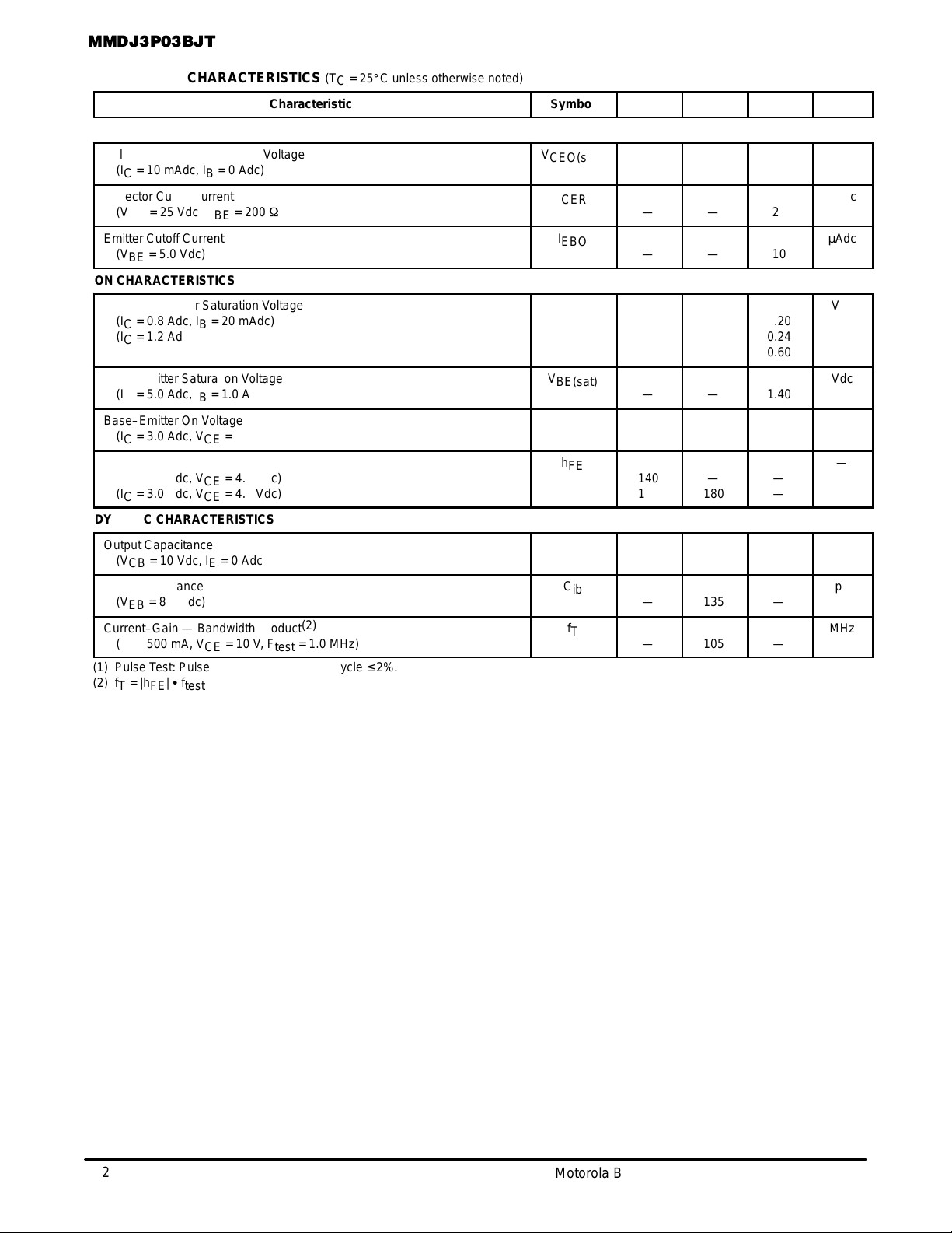
ELECTRICAL CHARACTERISTICS (T
Characteristic
OFF CHARACTERISTICS
ОООООООООООООООООООООООООООООООО
Collector–Emitter Sustaining Voltage
ОООООООООООООООООО
(IC = 10 mAdc, IB = 0 Adc)
Collector Cutoff Current
ОООООООООООООООООО
(VCE = 25 Vdc, RBE = 200 W)
Emitter Cutoff Current
(VBE = 5.0 Vdc)
ОООООООООООООООООО
ON CHARACTERISTICS
Collector–Emitter Saturation Voltage
(IC = 0.8 Adc, IB = 20 mAdc)
ОООООООООООООООООО
(IC = 1.2 Adc, IB = 20 mAdc)
(IC = 5.0 Adc, IB = 1.0 Adc)
ОООООООООООООООООО
Base–Emitter Saturation Voltage
(IC = 5.0 Adc, IB = 1.0 Adc)
ОООООООООООООООООО
Base–Emitter On Voltage
(IC = 3.0 Adc, VCE = 4.0 Vdc)
DC Current Gain
ОООООООООООООООООО
(IC = 1.2 Adc, VCE = 4.0 Vdc)
(IC = 3.0 Adc, VCE = 4.0 Vdc)
ОООООООООООООООООО
(1)
= 25_C unless otherwise noted)
C
Symbol
V
CEO(sus)
ÎÎ
I
CER
ÎÎ
I
EBO
ÎÎ
V
CE(sat)
ÎÎ
ÎÎ
V
BE(sat)
ÎÎ
V
BE(on)
h
FE
ÎÎ
ÎÎ
Min
ÎÎ
30
ÎÎ
—
—
ÎÎ
—
ÎÎ
—
—
ÎÎ
—
ÎÎ
—
ÎÎ
140
125
ÎÎ
Typ
ÎÎ
—
ÎÎ
—
—
ÎÎ
0.14
ÎÎ
—
—
ÎÎ
—
ÎÎ
—
ÎÎ
—
180
ÎÎ
Max
ÎÎ
—
ÎÎ
20
10
ÎÎ
0.20
ÎÎ
0.24
0.60
ÎÎ
1.40
ÎÎ
1.10
ÎÎ
—
—
ÎÎ
Unit
Vdc
ÎÎ
µAdc
ÎÎ
µAdc
ÎÎ
Vdc
ÎÎ
ÎÎ
Vdc
ÎÎ
Vdc
—
ÎÎ
ÎÎ
DYNAMIC CHARACTERISTICS
Output Capacitance
(VCB = 10 Vdc, IE = 0 Adc, f = 1.0 MHz)
ОООООООООООООООООО
Input Capacitance
ОООООООООООООООООО
(VEB = 8.0 Vdc)
Current–Gain — Bandwidth Product
ОООООООООООООООООО
(IC = 500 mA, VCE = 10 V, F
(2)
= 1.0 MHz)
test
C
ob
ÎÎ
C
ib
ÎÎ
f
T
ÎÎ
—
ÎÎ
ÎÎ
—
ÎÎ
—
100
ÎÎ
ÎÎ
135
ÎÎ
105
—
ÎÎ
ÎÎ
—
ÎÎ
—
pF
ÎÎ
pF
ÎÎ
MHz
ÎÎ
(1) Pulse Test: Pulse Width ≤ 300 µs, Duty Cycle ≤ 2%.
(2) fT = |hFE| S f
test
2
Motorola Bipolar Power Transistor Device Data
 Loading...