Motorola MMDFS2P102R2 Datasheet

1
Motorola TMOS Product Preview Data
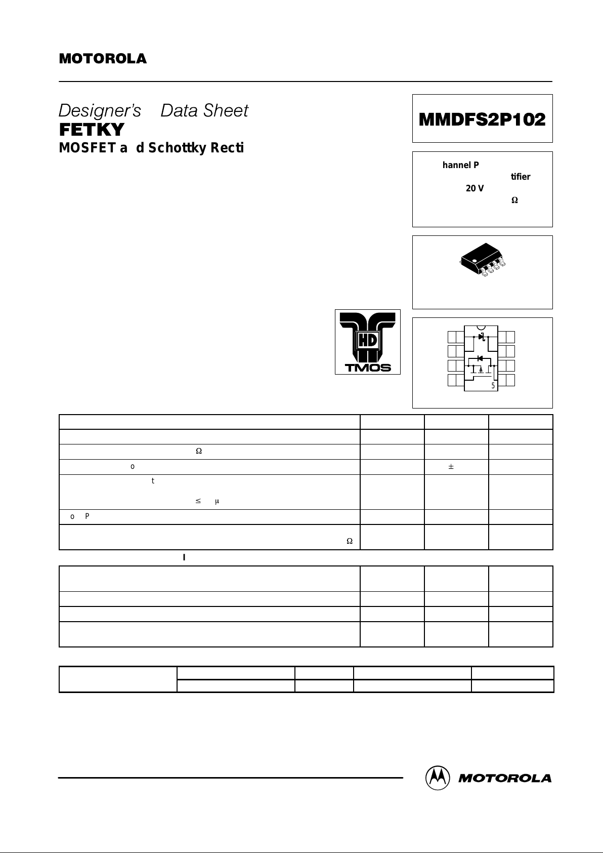
FETKY
MOSFET and Schottky Rectifier
The FETKY product family incorporates low R
DS(on)
, true logic level MOSFETs
packaged with industry leading, low forward drop, low leakage Schottky Barrier rectifiers
to offer high efficiency components in a space saving configuration. Independent pinouts
for TMOS and Schottky die allow the flexibility to use a single component for switching
and rectification functions in a wide variety of applications such as Buck Converter,
Buck–Boost, Synchronous Rectification, Low Voltage Motor Control, and Load Management in Battery Packs, Chargers, Cell Phones and other Portable Products.
• HDTMOS Power MOSFET with Low V
F
, Low IR Schottky Rectifier
• Lower Component Placement and Inventory Costs along with
Board Space Savings
• Logic Level Gate Drive — Can be Driven by Logic ICs
• Mounting Information for SO–8 Package Provided
• I
DSS
Specified at Elevated Temperature
• Applications Information Provided
MOSFET MAXIMUM RATINGS
(TJ = 25°C unless otherwise noted)
(1)
Rating
Symbol Value Unit
Drain–to–Source Voltage V
DSS
20 Vdc
Drain–to–Gate Voltage (RGS = 1.0 MW)
V
DGR
20 Vdc
Gate–to–Source Voltage — Continuous V
GS
"
20 Vdc
Drain Current
(3)
— Continuous @ TA = 25°C
— Continuous @ TA = 100°C
— Single Pulse (tp v 10 ms)
I
D
I
D
I
DM
3.3
2.1
20
Adc
Apk
Total Power Dissipation @ TA = 25°C
(2)
P
D
2.0 Watts
Single Pulse Drain–to–Source Avalanche Energy — STAR TING TJ = 25°C
VDD = 30 Vdc, VGS = 5.0 Vdc, VDS = 20 Vdc, IL = 9.0 Apk, L = 10 mH, RG = 25
W
E
AS
324 mJ
SCHOTTKY RECTIFIER MAXIMUM RATINGS (T
J
= 25°C unless otherwise noted)
Peak Repetitive Reverse Voltage
DC Blocking Voltage
V
RRM
V
R
20 Volts
Average Forward Current
(3)
(Rated VR) TA = 100°C I
O
1.0 Amps
Peak Repetitive Forward Current
(3)
(Rated VR, Square Wave, 20 kHz) TA = 105°C I
frm
2.0 Amps
Non–Repetitive Peak Surge Current
(Surge applied at rated load conditions, halfwave, single phase, 60 Hz)
I
fsm
20 Amps
DEVICE MARKING ORDERING INFORMATION
Device Reel Size Tape Width Quantity
2P102
MMDFS2P102R2 13″ 12 mm embossed tape 2500 units
(1) Negative sign for P–channel device omitted for clarity.
(2) Pulse Test: Pulse Width ≤ 250 µs, Duty Cycle ≤ 2.0%.
(3) Mounted on 2″ square FR4 board (1″ sq. 2 oz. Cu 0.06″ thick single sided), 10 sec. max.
Designer’s Data for “Worst Case” Conditions— The Designer’s Data Sheet permits the design of most circuits entirely from the information presented. SOA Limit
curves — representing boundaries on device characteristics — are given to facilitate “worst case” design.
HDTMOS and Designer’s are trademarks of Motorola, Inc. TMOS is a registered trademark of Motorola, Inc.
FETKY is a trademark of International Rectifier.
Order this document
by MMDFS2P102/D
MOTOROLA
SEMICONDUCTOR TECHNICAL DATA
MMDFS2P102
P–Channel Power MOSFET
with Schottky Rectifier
20 Volts
R
DS(on)
= 0.16
W
VF = 0.39 Volts
CASE 751–05, Style 18
(SO–8)
1
2
3
4
8
7
6
5
A
A
S
G
C
C
D
D
TOP VIEW
Motorola, Inc. 1997

MMDFS2P102
2
Motorola TMOS Product Preview Data
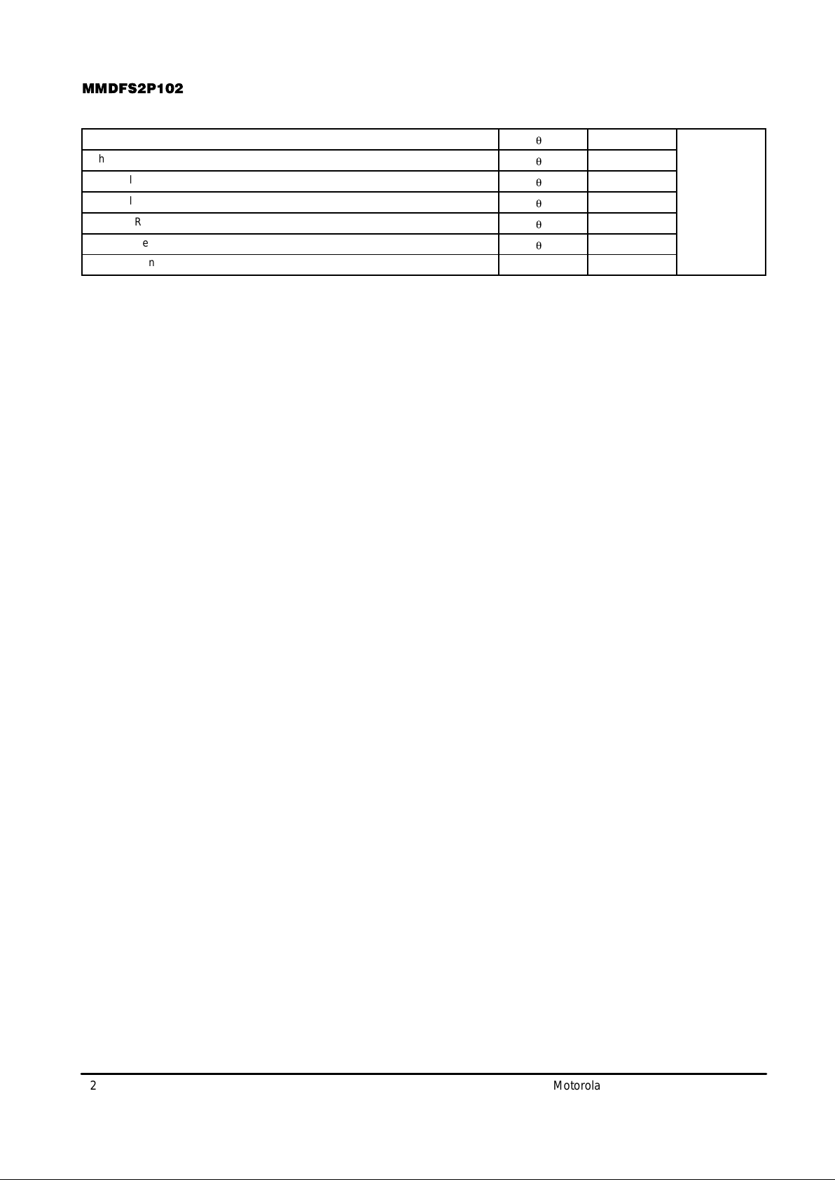
THERMAL CHARACTERISTICS — SCHOTTKY AND MOSFET
Thermal Resistance — Junction–to–Ambient
(1)
— MOSFET
R
q
JA
167
°C/W
Thermal Resistance — Junction–to–Ambient
(2)
— MOSFET
R
q
JA
100
Thermal Resistance — Junction–to–Ambient
(3)
— MOSFET
R
q
JA
62.5
Thermal Resistance — Junction–to–Ambient
(1)
— Schottky
R
q
JA
204
Thermal Resistance — Junction–to–Ambient
(2)
— Schottky
R
q
JA
122
Thermal Resistance — Junction–to–Ambient
(3)
— Schottky
R
q
JA
83
Operating and Storage Temperature Range Tj, T
stg
–55 to 150
(1) Mounted with minimum recommended pad size, PC Board FR4.
(2) Mounted on 2″ square FR4 board (1″ sq. 2 oz. Cu 0.06″ thick single sided), Steady State.
(3) Mounted on 2″ square FR4 board (1″ sq. 2 oz. Cu 0.06″ thick single sided), 10 sec. max.

MMDFS2P102
3
Motorola TMOS Product Preview Data
MOSFET ELECTRICAL CHARACTERISTICS (T
J
= 25°C unless otherwise noted)
(1)
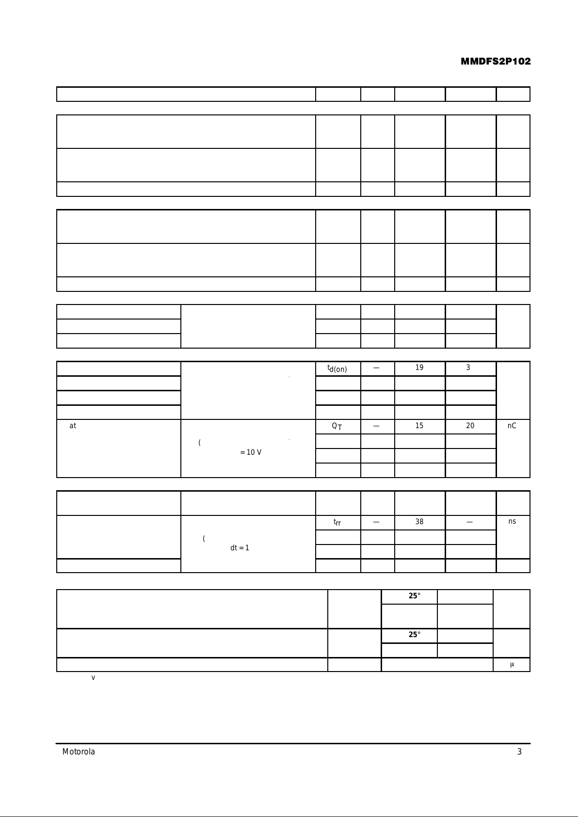
Characteristic
Symbol Min Typ Max Unit
OFF CHARACTERISTICS
Drain–Source Voltage
(VGS = 0 Vdc, ID = 0.25 mA)
T emperature Coef ficient (Positive)
V
(BR)DSS
20
—
—
25
—
—
Vdc
mV/°C
Zero Gate Drain Current
(VDS = 30 Vdc, VGS = 0 Vdc)
(VDS = 20 Vdc, VGS = 0 Vdc, TJ = 125°C)
I
DSS
—
—
—
—
1.0
10
µAdc
Gate Body Leakage Current (VGS = ± 20 Vdc, VDS = 0) I
GSS
— — 100 nAdc
ON CHARACTERISTICS
(2)
Gate Threshold Voltage
(VDS = VGS, ID = 0.25 mA)
T emperature Coef ficient (Negative)
V
GS(th)
1.0
—
1.5
4.0
2.0
—
Vdc
mV/°C
Static Drain–Source Resistance
(VGS = 10 Vdc, ID = 2.0 Adc)
(VGS = 4.5 Vdc, ID = 2.5 Adc)
R
DS(on)
—
—
0.118
0.152
0.160
0.180
Ohms
Forward Transconductance (VDS = 3.0 Vdc, ID = 1.0 Adc) g
FS
2.0 3.0 — mhos
DYNAMIC CHARACTERISTICS
Input Capacitance
C
iss
— 420 588 pF
Output Capacitance
(VDS = 16 Vdc, VGS = 0 Vdc,
f = 1.0 MHz
)
C
oss
— 290 406
Reverse Transfer Capacitance
f = 1.0 MHz)
C
rss
— 116 232
SWITCHING CHARACTERISTICS
(3)
Turn–On Delay Time
t
d(on)
— 19 38 ns
Rise Time
(VDS = 10 Vdc, ID = 2.0 Adc,
t
r
— 66 132
Turn–Off Delay Time
V
GS
= 4.5 Vdc,
RG = 6.0 Ω)
t
d(off)
— 25 50
Fall Time
G
)
t
f
— 37 74
Gate Charge
Q
T
— 15 20
nC
(VDS = 16 Vdc, ID = 2.0 Adc,
Q
1
— 1.2 —
(
DS
,
D
,
VGS = 10 Vdc)
Q
2
— 5.0 —
Q
3
— 4.0 —
DRAIN SOURCE DIODE CHARACTERISTICS
Forward On–Voltage
(2)
(IS = 2.0 Adc,
VGS = 0 Vdc)
V
SD
— 1.5 2.1
V
Reverse Recovery Time
t
rr
— 38 —
ns
(IS = 2.0 Adc, VDD = 15 V,
t
a
— 17 —
(
S
,
DD
,
dIS/dt = 100 A/µs)
t
b
— 21 —
Reverse Recovery Stored Charge Q
RR
— 0.034 — µC
SCHOTTKY RECTIFIER ELECTRICAL CHARACTERISTICS (T
J
= 25°C unless otherwise noted)
Maximum Instantaneous Forward Voltage
(2)
V
F
TJ = 25°C TJ = 125°C
Volts
IF = 1.0 A
IF = 2.0 A
0.47
0.58
0.39
0.53
Maximum Instantaneous Reverse Current
(2)
I
R
TJ = 25°C TJ = 125°C
mA
VR = 20 V
0.05 10
Maximum Voltage Rate of Change VR = 20 V dV/dt 10,000
V/ms
(1) Negative sign for P–channel device omitted for clarity.
(2) Pulse Test: Pulse Width ≤ 300 µsec, Duty Cycle ≤ 2.0%.
(3) Switching characteristics are independent of operating temperature.

MMDFS2P102
4
Motorola TMOS Product Preview Data
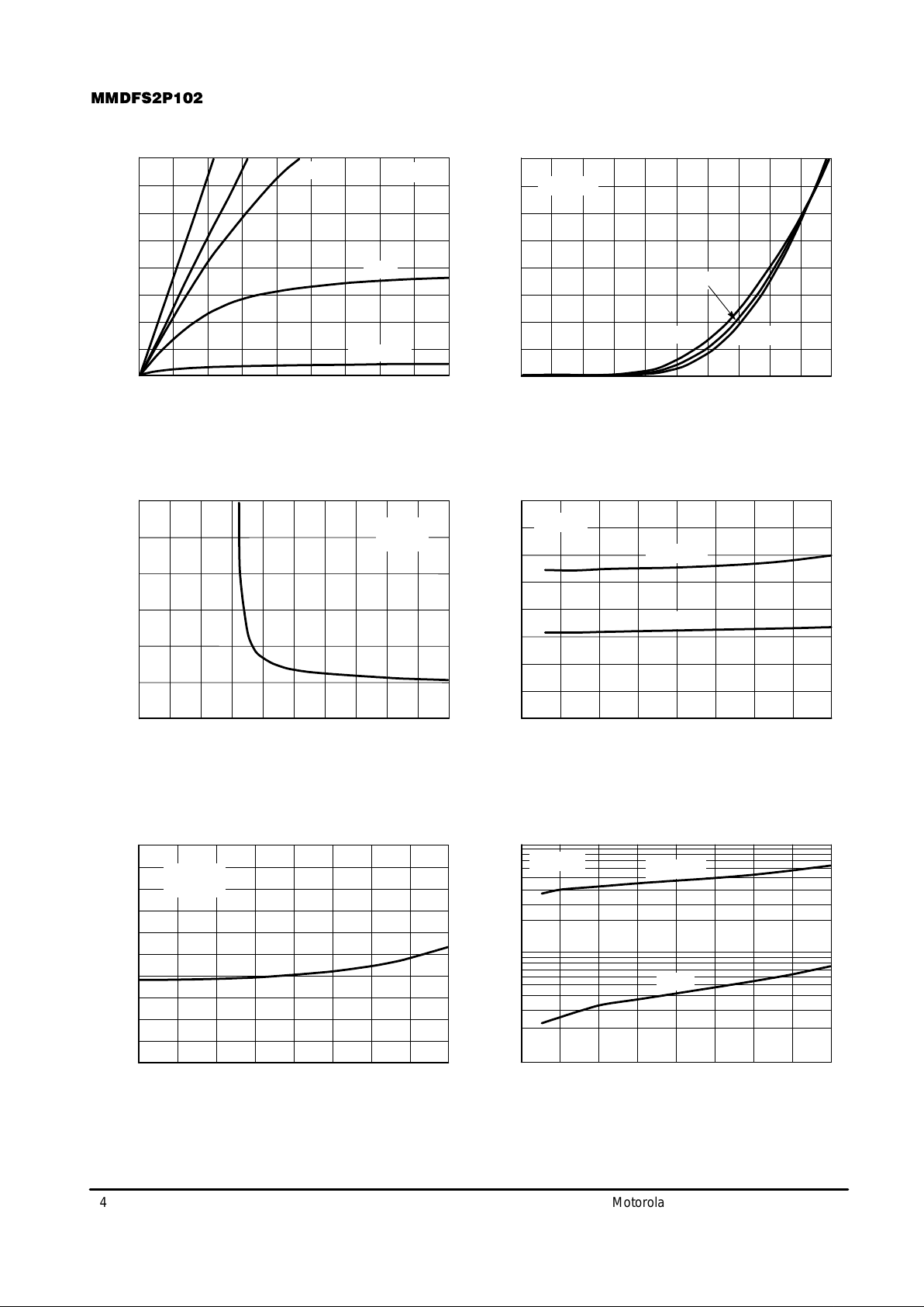
TYPICAL FET ELECTRICAL CHARACTERISTICS
Figure 1. On–Region Characteristics Figure 2. Transfer Characteristics
Figure 3. On–Resistance versus
Gate–T o–Source Voltage
Figure 4. On–Resistance versus Drain Current
and Gate Voltage
Figure 5. On–Resistance Variation with
Temperature
Figure 6. Drain–To–Source Leakage
Current versus Voltage
1.20
VDS, DRAIN–TO–SOURCE VOL TAGE (VOLTS)
4.0
3.0
2.0
VGS, GATE–T O–SOURCE VOLT AGE (VOLTS)
3.51.0
3.0
2.0
1.0
0
8.0 100
VGS, GATE–T O–SOURCE VOLT AGE (VOLTS)
0.6
0.4
0.3
0.2
0.1
0
ID, DRAIN CURRENT (AMPS)
0.50
0.20
0.16
0.12
0.08
0.04
1.0
–25 25–50
TJ, JUNCTION TEMPERATURE (
°
C)
1.2
0.8
0.6
VDS, DRAIN–TO–SOURCE VOL TAGE (VOLTS)
5.0 200
100
1.0
150
I
D
, DRAIN CURRENT (AMPS)
I
R
1.0
0
0.60.2 0.4 0.8 1.0 1.4 1.6 1.5 2.0 2.5 3.0
4.0
2.0 4.0 6.0 1.5 2.0 2.5 3.0 3.5 4.0
, DRAIN–TO–SOURCE RESIST ANCE (NORMALIZED)R
DS(on)
50 10075
1.0
10
10
I
DSS
, LEAKAGE (nA)
1.8
, DRAIN CURRENT (AMPS)
D
, DRAIN–TO–SOURCE RESIST ANCE (OHMS)
DS(on)
0.5
R , DRAIN–TO–SOURCE RESIST ANCE (OHMS)
DS(on)
125 150
1.4
1.6
VGS = 10 V
ID = 2.0 A
VGS = 0 V
TJ = 125°C
100°C
TJ = 25°C
VGS = 4.5 V
10 V
TJ = 25°C
ID = 1.0 A
VDS ≥ 10 V
TJ = –55°C
100°C
25°C
TJ = 25°C
3.1 V
VGS = 2.4 V
10 V
4.5 V
3.8 V
 Loading...