

Motorola MMDF4C03HDR2 Datasheet
1
Motorola TMOS Power MOSFET Transistor Device Data
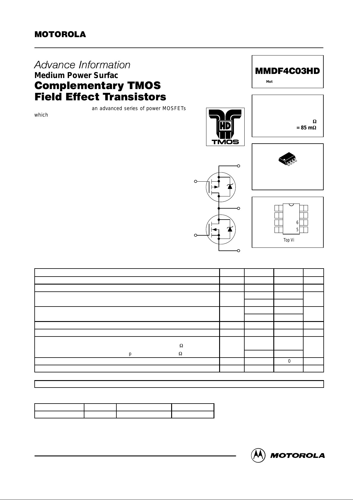
Medium Power Surface Mount Products
MiniMOS devices are an advanced series of power MOSFETs
which utilize Motorola’s High Cell Density HDTMOS process.
These miniature surface mount MOSFET s feature ultra low R
DS(on)
and true logic level performance. They are capable of withstanding
high energy in the avalanche and commutation modes and the
drain–to–source diode has a very low reverse recovery time.
MiniMOS devices are designed for use in low voltage, high speed
switching applications where power efficiency is important. Typical
applications are dc–dc converters, and power management in
portable and battery powered products such as computers,
printers, cellular and cordless phones. They can also be used for
low voltage motor controls in mass storage products such as disk
drives and tape drives.
• Ultra Low R
DS(on)
Provides Higher Efficiency and
Extends Battery Life
• Logic Level Gate Drive — Can Be Driven by Logic ICs
• Miniature SO–8 Surface Mount Package —
Saves Board Space
• Ideal for Synchronous Rectification
• Diode Exhibits High Speed, With Soft Recovery
• I
DSS
Specified at Elevated Temperature
• Mounting Information for SO–8 Package Provided
MAXIMUM RATINGS
(TJ = 25°C unless otherwise noted)
Rating
Symbol Polarity Value Unit
Drain–to–Source Voltage V
DSS
— 30 Vdc
Gate–to–Source Voltage V
GS
— ± 20 Vdc
Drain Current — Continuous I
D
N–Channel 5.5 Adc
P–Channel 4.4
Drain Current — Pulsed I
DM
N–Channel 25 Apk
P–Channel 20
Operating and Storage Temperature Range TJ, T
stg
— –55 to +150 °C
Total Power Dissipation @ TA = 25°C
(1)
P
D
2.5 Watts
Single Pulse Drain–to–Source Avalanche Energy — Starting TJ = 25°C
(VDD = 30 Vdc, VGS = 5.0 Vdc, IL = 9.0 Apk, L = 10 mH, RG = 25 W)
E
AS
N–Channel 325
mJ
(VDD = 30 Vdc, VGS = 5.0 Vdc, IL = 9.0 Apk, L = 10 mH, RG = 25 W)
P–Channel 450
Thermal Resistance — Junction–to–Ambient
(1)
R
θJA
50 °C/W
Maximum Lead Temperature for Soldering Purposes, 1/8″ from Case for 10 sec. T
L
260 °C
DEVICE MARKING
D4C03
(1) Mounted on G10/FR4 glass epoxy board using minimum recommended footprint.
ORDERING INFORMATION
Device Reel Size Tape Width Quantity
MMDF4C03HDR2 13″ 12 mm embossed tape 2500
This document contains information on a new product. Specifications and information herein are subject to change without notice.
HDTMOS and MiniMOS are trademarks of Motorola, Inc. TMOS is a registered trademark of Motorola, Inc.
Thermal Clad is a trademark of the Bergquist Company.
Preferred devices are Motorola recommended choices for future use and best overall value.
Order this document
by MMDF4C03HD/D
SEMICONDUCTOR TECHNICAL DATA
Motorola, Inc. 1997
N–Source
1
2
3
4
8
7
6
5
Top View
N–Gate
P–Source
P–Gate
Drain
Drain
Drain
Drain
P–G
CASE 751–05, Style 11
SO–8
COMPLEMENTARY
DUAL TMOS POWER FET
30 VOLTS
N–CH R
DS(on)
= 50 m
W
P–CH R
DS(on)
= 85 m
W
Motorola Preferred Device
N–S
D
P–S
N–G
REV 1
MMDF4C03HD
2
Motorola TMOS Power MOSFET Transistor Device Data
ELECTRICAL CHARACTERISTICS
(TA = 25°C unless otherwise noted)
Characteristic Symbol Polarity Min Typ Max Unit
OFF CHARACTERISTICS
Drain–to–Source Breakdown Voltage
(VGS = 0 Vdc, ID = 0.25 mAdc)
V
(BR)DSS
— 30 — —
Vdc
Zero Gate Voltage Drain Current
(VDS = 30 Vdc, VGS = 0 Vdc)
I
DSS
(N)
(P)
—
—
—
—
1.0
1.0
µAdc
Gate–Body Leakage Current (VGS = ±20 Vdc, VDS = 0) I
GSS
— — — ±100 nAdc
ON CHARACTERISTICS
(1)
Gate Threshold Voltage (VDS = VGS, ID = 250 µAdc)
Threshold Temperature Coefficient (Negative)
V
GS(th)
—
—
1.0
—
—
—
—
—
Vdc
mV/°C
Drain–to–Source On–Resistance (VGS = 10 Vdc, ID = 3.5 Adc)
(VGS = 10 Vdc, ID = 3.5 Adc)
R
DS(on)
1 (N)
(P)
—
—
0.037
0.075
0.05
0.085
Ohms
Static Drain–to–Source On–Resistance
(VGS = 4.5 Vdc, ID = 2.5 Adc)
(VGS = 4.5 Vdc, ID = 2.0 Adc)
R
DS(on)
2
(N)
(P)
—
—
0.55
0.125
0.08
0.16
Ohms
Forward Transconductance
(VDS = 15 Vdc, ID = 3.5 Adc)
g
FS
(N)
(P)
—
—
9.0
6.0
—
—
mhos
DYNAMIC CHARACTERISTICS
Input Capacitance
C
iss
(N)
(P)
—
—
430
425
600
600
pF
Output Capacitance
(VDS = 24 Vdc,
VGS = 0 Vdc,
f = 1.0 MHz
)
C
oss
(N)
(P)
—
—
217
209
300
300
Transfer Capacitance
f = 1.0 MHz)
C
rss
(N)
(P)
—
—
67.5
57.2
135
80
SWITCHING CHARACTERISTICS
(2)
Turn–On Delay Time
t
d(on)
(N)
(P)
—
—
8.2
11.7
16.4
23.4
ns
Rise Time
(VDD = 15 Vdc,
ID = 1.0 Adc,
t
r
(N)
(P)
—
—
8.48
15.8
16.9
31.6
Turn–Off Delay Time
D
,
VGS = 10 Vdc,
RG = 6.0 Ω)
t
d(off)
(N)
(P)
—
—
89.6
167.3
179
334.6
Fall Time t
f
(N)
(P)
—
—
61.1
102.6
122
205.2
Total Gate Charge
(See Figure 8)
Q
T
(N)
(P)
—
—
15.7
14.8
31.4
29.6
nC
(VDS = 10 Vdc,
Q
1
(N)
(P)
—
—
2.0
1.7
—
—
I
D
=
3.5 Ad
c,
VGS = 10 Vdc)
Q
2
(N)
(P)
—
—
4.6
4.7
—
—
Q
3
(N)
(P)
—
—
3.9
3.4
—
—
SOURCE–DRAIN DIODE CHARACTERISTICS
Forward On–Voltage
(2)
(IS = 1.7 Adc, VGS = 0 Vdc)
(IS = –1.7 Adc, VGS = 0 Vdc)
V
SD
(N)
(P)
—
—
0.77
0.90
1.2
1.2
Vdc
Reverse Recovery Time
(N)
(ID = 3.5 Adc,
t
rr
(N)
(P)
—
—
54.5
77.4
—
—
ns
(
D
,
VGS = 0 Vdc
dIS/dt = 100 A/µs)
t
a
(N)
(P)
—
—
14.8
19.9
—
—
(P)
(ID = 3.5 Adc,
t
b
(N)
(P)
—
—
39.7
57.5
—
—
Reverse Recovery Stored Charge
(
D
,
VGS = 0 Vdc
dIS/dt = 100 A/µs)
Q
RR
(N)
(P)
—
—
0.048
0.088
—
—
µC
(1) Pulse Test: Pulse Width ≤ 300 µs, Duty Cycle ≤ 2%.
(2) Switching characteristics are independent of operating junction temperature.
MMDF4C03HD
3
Motorola TMOS Power MOSFET Transistor Device Data
TYPICAL ELECTRICAL CHARACTERISTICS
N–Channel P–Channel
Figure 1. On–Region Characteristics
Figure 2. Transfer Characteristics
Figure 1. On–Region Characteristics
Figure 2. Transfer Characteristics
Figure 3. On–Resistance versus
Gate–T o–Source Voltage
Figure 3. On–Resistance versus
Gate–T o–Source Voltage
2.9 V
1.2 2.00
VDS, DRAIN–TO–SOURCE VOL TAGE (VOL TS)
6.0
4.0
5.0
3.0
I
D
, DRAIN CURRENT (AMPS)
2.0
1.0
0
0.60.2 0.4 0.8 1.0 1.4 1.6 1.8
TJ = 25°C
2.7 V
3.1 V
3.3 V
3.5 V
3.7 V
3.9 V
VGS = 10 V
4.1 V
4.5 V
6.0 V
4.3 V
VGS, GATE–T O–SOURCE VOLTAGE (VOLTS)
4.5 5.01.5
4.0
2.0
1.0
0
I
2.0 2.5 3.0 3.5 4.0
3.0
5.0
6.0
, DRAIN CURRENT (AMPS)
D
VDS ≥ 10 V
TJ = –55°C
100°C
25°C
8.0 102.0
VGS, GATE–T O–SOURCE VOLTAGE (VOLTS)
0.8
0.4
0.3
0.2
0.1
0
9.0
R
3.0 4.0 5.0 6.0 7.0
, DRAIN–TO–SOURCE RESIST ANCE (OHMS)
DS(on)
0.5
TJ = 25°C
ID = 3 A
0.6
0.7
1.2 2.00
VDS, DRAIN–TO–SOURCE VOL TAGE (VOL TS)
12
8.0
10
6.0
I
D
, DRAIN CURRENT (AMPS)
4.0
2.0
0
0.60.2 0.4 0.8 1.0 1.4 1.6 1.8
TJ = 25°C
2.7 V
2.9 V
3.1 V
3.3 V
3.5 V
VGS = 2.5 V
10 V
6.0 V
4.5 V
4.3 V
4.1 V
3.7 V
3.9 V
VGS, GATE–T O–SOURCE VOLTAGE (VOLTS)
4.5 5.01.5
8.0
4.0
2.0
0
I
2.0 2.5 3.0 3.5 4.0
6.0
10
12
, DRAIN CURRENT (AMPS)
D
VDS ≥ 10 V
TJ = –55°C
100°C
25°C
8.0 102.0
VGS, GATE–T O–SOURCE VOLTAGE (VOLTS)
0.30
0.20
0.15
0.10
0.05
0
9.0
R
3.0 4.0 5.0 6.0 7.0
, DRAIN–TO–SOURCE RESIST ANCE (OHMS)
DS(on)
0.25
TJ = 25°C
ID = 6 A
MMDF4C03HD
4
Motorola TMOS Power MOSFET Transistor Device Data
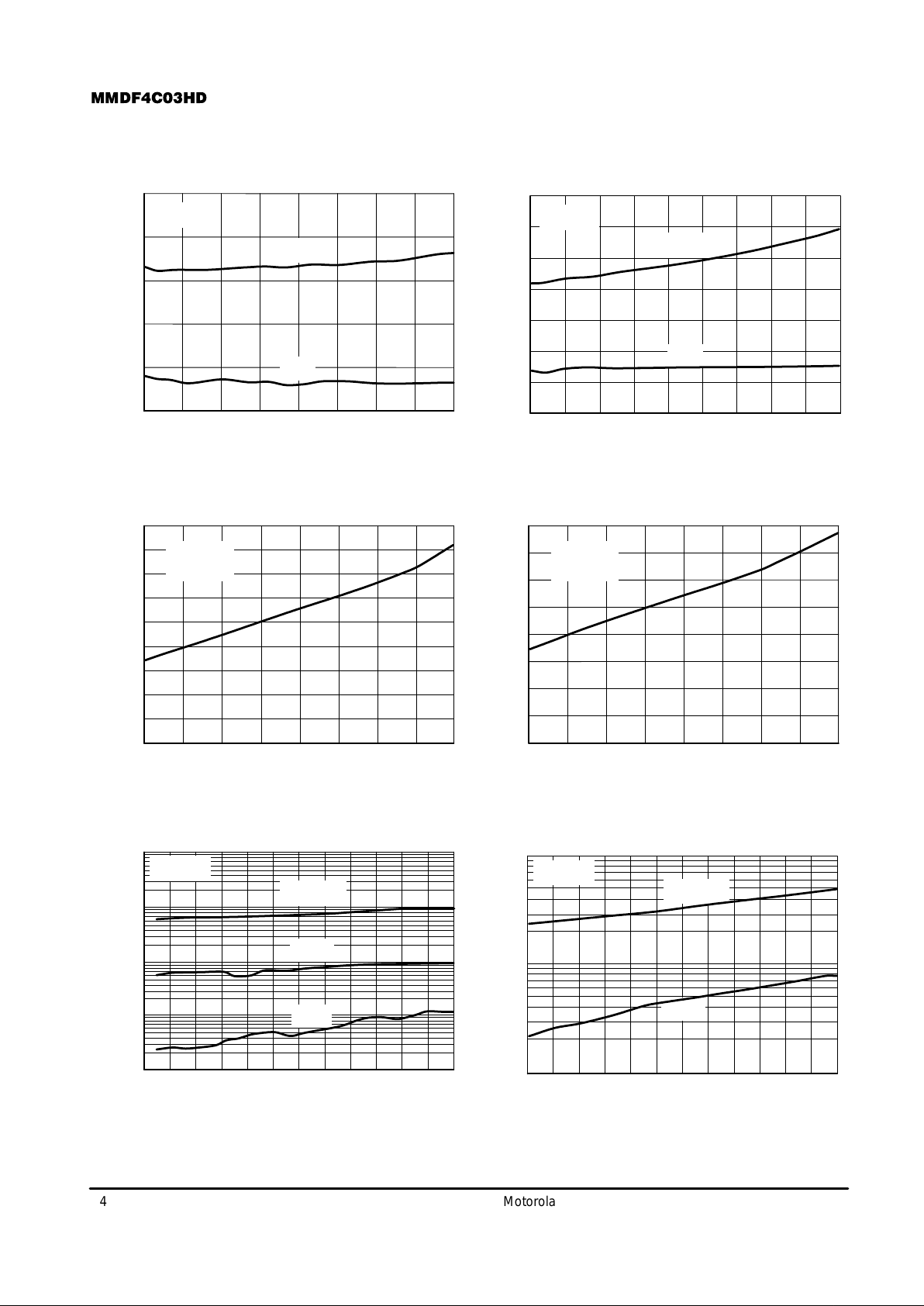
TYPICAL ELECTRICAL CHARACTERISTICS
N–Channel P–Channel
Figure 4. On–Resistance versus Drain Current
and Gate Voltage
Figure 5. On–Resistance Variation with
Temperature
Figure 6. Drain–To–Source Leakage
Current versus Voltage
Figure 4. On–Resistance versus Drain Current
and Gate Voltage
Figure 5. On–Resistance Variation with
Temperature
Figure 6. Drain–To–Source Leakage
Current versus Voltage
ID, DRAIN CURRENT (AMPS)
1.51.0
0.18
0.12
0.10
0.08
0.06
0.04
2.0 4.0 5.53.0 4.5 5.02.5
R , DRAIN–TO–SOURCE RESISTANCE (OHMS)
DS(on)
TJ = 25°C
VGS = 4.5 V
10 V
3.5
0.16
0.14
–25 25–50
TJ, JUNCTION TEMPERATURE (
°
C)
1.2
0.8
0.6
0.4
0.2
0
0
, DRAIN–TO–SOURCE RESIST ANCE (NORMALIZED)R
DS(on)
50 10075
1.0
125 150
1.6
1.4
VGS = 10 V
ID = 1.5 A
VDS, DRAIN–TO–SOURCE VOL TAGE (VOL TS)
5.0 300
100
1.0
1510 20 25
10
I
DSS
, LEAKAGE (nA)
VGS = 0 V
TJ = 125°C
100°C
ID, DRAIN CURRENT (AMPS)
2.01.0
0.050
0.045
0.040
0.035
0.030
0.025
3.0 4.0 5.0 6.0 7.0 8.0 9.0
R , DRAIN–TO–SOURCE RESISTANCE (OHMS)
DS(on)
TJ = 25°C
VGS = 4.5 V
10 V
–25 25–50
TJ, JUNCTION TEMPERATURE (
°
C)
1.2
0.8
0.6
0.4
0.2
0
0
, DRAIN–TO–SOURCE RESIST ANCE (NORMALIZED)R
DS(on)
50 10075
1.0
125 150
1.6
1.4
1.8
VGS = 10 V
ID = 3 A
VDS, DRAIN–TO–SOURCE VOL TAGE (VOL TS)
5.0 300
1000
100
1.0
0.1
1510 20 25
10
I
DSS
, LEAKAGE (nA)
VGS = 0 V
TJ = 125°C
100°C
25°C
 Loading...