

Motorola MMBT6427LT1 Datasheet
1
Motorola Small–Signal Transistors, FETs and Diodes Device Data
NPN Silicon
MAXIMUM RATINGS
Rating Symbol Value Unit
Collector–Emitter Voltage V
CEO
40 Vdc
Collector–Base Voltage V
CBO
40 Vdc
Emitter–Base Voltage V
EBO
12 Vdc
Collector Current — Continuous I
C
500 mAdc
THERMAL CHARACTERISTICS
Characteristic Symbol Max Unit
Total Device Dissipation FR–5 Board
(1)
TA = 25°C
Derate above 25°C
P
D
225
1.8
mW
mW/°C
Thermal Resistance, Junction to Ambient
R
q
JA
556 °C/W
Total Device Dissipation
Alumina Substrate,
(2)
TA = 25°C
Derate above 25°C
P
D
300
2.4
mW
mW/°C
Thermal Resistance, Junction to Ambient
R
q
JA
417 °C/W
Junction and Storage Temperature TJ, T
stg
–55 to +150 °C
DEVICE MARKING
MMBT6427LT1 = 1V
ELECTRICAL CHARACTERISTICS (T
A
= 25°C unless otherwise noted)
Characteristic
Symbol Min Max Unit
OFF CHARACTERISTICS
Collector–Emitter Breakdown Voltage
(IC = 10 mAdc, VBE = 0)
V
(BR)CEO
40 —
Vdc
Collector–Base Breakdown Voltage
(IC = 100 mAdc, IE = 0)
V
(BR)CBO
40 —
Vdc
Emitter–Base Breakdown Voltage
(IC = 10 mAdc, IC = 0)
V
(BR)EBO
12 —
Vdc
Collector Cutoff Current
(VCE = 25 Vdc, IB = 0)
I
CES
— 1.0
µAdc
Collector Cutoff Current
(VCB = 30 Vdc, IE = 0)
I
CBO
— 50
nAdc
Emitter Cutoff Current
(VEB = 10 Vdc, IC = 0)
I
EBO
— 50
nAdc
1. FR–5 = 1.0 0.75 0.062 in.
2. Alumina = 0.4 0.3 0.024 in. 99.5% alumina.
Thermal Clad is a trademark of the Bergquist Company.
Preferred devices are Motorola recommended choices for future use and best overall value.
Order this document
by MMBT6427LT1/D
SEMICONDUCTOR TECHNICAL DATA
Motorola Preferred Device
1
2
3
CASE 318–08, STYLE 6
SOT–23 (TO–236AB)
Motorola, Inc. 1996
COLLECTOR 3
BASE
1
EMITTER 2
MMBT6427LT1
2
Motorola Small–Signal Transistors, FETs and Diodes Device Data
ELECTRICAL CHARACTERISTICS (T
A
= 25°C unless otherwise noted) (Continued)
Characteristic
Symbol Min Max Unit
ON CHARACTERISTICS
DC Current Gain
(IC = 10 mAdc, VCE = 5.0 Vdc)
(IC = 100 mAdc, VCE = 5.0 Vdc)
(IC = 500 mAdc, VCE = 5.0 Vdc)
h
FE
10,000
20,000
14,000
100,000
200,000
140,000
—
Collector–Emitter Saturation Voltage
(IC = 50 mAdc, IB = 0.5 mAdc)
(IC = 500 mAdc, IB = 0.5 mAdc)
V
CE(sat)
(3)
—
—
1.2
1.5
Vdc
Base–Emitter Saturation Voltage
(IC = 500 mAdc, IB = 0.5 mAdc)
V
BE(sat)
— 2.0
Vdc
Base–Emitter On Voltage
(IC = 50 mAdc, VCE = 5.0 Vdc)
V
BE(on)
— 1.75
Vdc
SMALL–SIGNAL CHARACTERISTICS
Output Capacitance
(VCB = 10 Vdc, IE = 0, f = 1.0 MHz)
C
obo
— 7.0
pF
Input Capacitance
(VEB = 0.5 Vdc, IC = 0, f = 1.0 MHz)
C
ibo
— 15
pF
CurrentGain — High Frequency
(IC = 10 mAdc, VCE = 5.0 Vdc, f = 100 MHz)
|hfe|
1.3 —
Vdc
Noise Figure
(IC = 1.0 mAdc, VCE = 5.0 Vdc, RS = 100 kΩ, f = 1.0 kHz)
NF
— 10
dB
3. Pulse Test: Pulse Width = 300 ms, Duty Cycle = 2.0%.
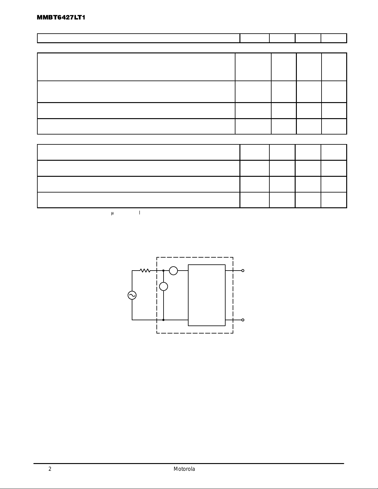
R
S
i
n
e
n
IDEAL
TRANSISTOR
Figure 1. Transistor Noise Model
MMBT6427LT1
3
Motorola Small–Signal Transistors, FETs and Diodes Device Data
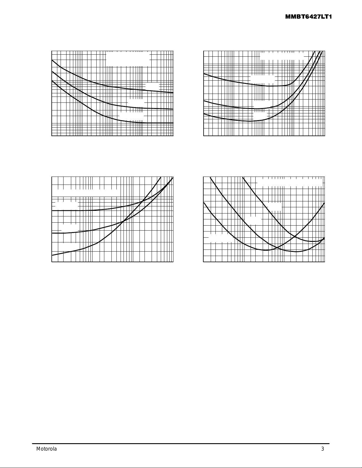
NOISE CHARACTERISTICS
(VCE = 5.0 Vdc, TA = 25°C)
Figure 2. Noise Voltage
f, FREQUENCY (Hz)
50
100
200
500
20
Figure 3. Noise Current
f, FREQUENCY (Hz)
Figure 4. Total Wideband Noise Voltage
RS, SOURCE RESISTANCE (kΩ)
Figure 5. Wideband Noise Figure
RS, SOURCE RESISTANCE (kΩ)
5.0
50
70
100
200
30
10
20
1.0
101020 50 100 200 500 1 k 2 k 5 k 10 k 20 k 50 k 100 k
2.0
1.0
0.7
0.5
0.3
0.2
0.1
0.07
0.05
0.03
0.02
BANDWIDTH = 1.0 Hz
RS
≈
0
IC = 1.0 mA
100 µA
10 µA
BANDWIDTH = 1.0 Hz
IC = 1.0 mA
100 µA
10 µA
e
n
, NOISE VOLTAGE (nV)
i
n
, NOISE CURRENT (pA)
2.0 5.0 10 20 50 100 200 500 100
0
BANDWIDTH = 10 Hz TO 15.7 kHz
IC = 10 µA
100 µA
1.0 mA
8.0
10
12
14
6.0
0
4.0
1.0 2.0 5.0 10 20 50 100 200 500 100
0
2.0
BANDWIDTH = 10 Hz TO 15.7 kHz
10 µA
100 µA
IC = 1.0 mA
V
T
, TOTAL WIDEBAND NOISE VOLTAGE (nV)
NF, NOISE FIGURE (dB)
10 20 50 100 200 500 1 k 2 k 5 k 10 k 20 k 50 k 100 k
 Loading...