

Motorola MMBT5401LT1 Datasheet
1
Motorola Small–Signal Transistors, FETs and Diodes Device Data
PNP Silicon
MAXIMUM RATINGS
Rating Symbol Value Unit
Collector–Emitter Voltage V
CEO
–150 Vdc
Collector–Base Voltage V
CBO
–160 Vdc
Emitter–Base Voltage V
EBO
–5.0 Vdc
Collector Current — Continuous I
C
–500 mAdc
THERMAL CHARACTERISTICS
Characteristic Symbol Max Unit
Total Device Dissipation FR–5 Board
(1)
TA = 25°C
Derate above 25°C
P
D
225
1.8
mW
mW/°C
Thermal Resistance, Junction to Ambient
R
q
JA
556 °C/W
Total Device Dissipation
Alumina Substrate,
(2)
TA = 25°C
Derate above 25°C
P
D
300
2.4
mW
mW/°C
Thermal Resistance, Junction to Ambient
R
q
JA
417 °C/W
Junction and Storage Temperature TJ, T
stg
–55 to +150 °C
DEVICE MARKING
MMBT5401LT1 = 2L
ELECTRICAL CHARACTERISTICS (T
A
= 25°C unless otherwise noted)
Characteristic
Symbol Min Max Unit
OFF CHARACTERISTICS
Collector–Emitter Breakdown Voltage
(IC = –1.0 mAdc, IB = 0)
V
(BR)CEO
–150 —
Vdc
Collector–Base Breakdown Voltage
(IC = –100 mAdc, IE = 0)
V
(BR)CBO
–160 —
Vdc
Emitter–Base Breakdown Voltage
(IE = –10 mAdc, IC = 0)
V
(BR)EBO
–5.0 —
Vdc
Collector Cutoff Current
(VCB = –120 Vdc, IE = 0)
(VCB = –120 Vdc, IE = 0, TA = 100°C)
I
CES
—
—
–50
–50
nAdc
µAdc
1. FR–5 = 1.0 0.75 0.062 in.
2. Alumina = 0.4 0.3 0.024 in. 99.5% alumina.
Thermal Clad is a trademark of the Bergquist Company
Preferred devices are Motorola recommended choices for future use and best overall value.
Order this document
by MMBT5401LT1/D
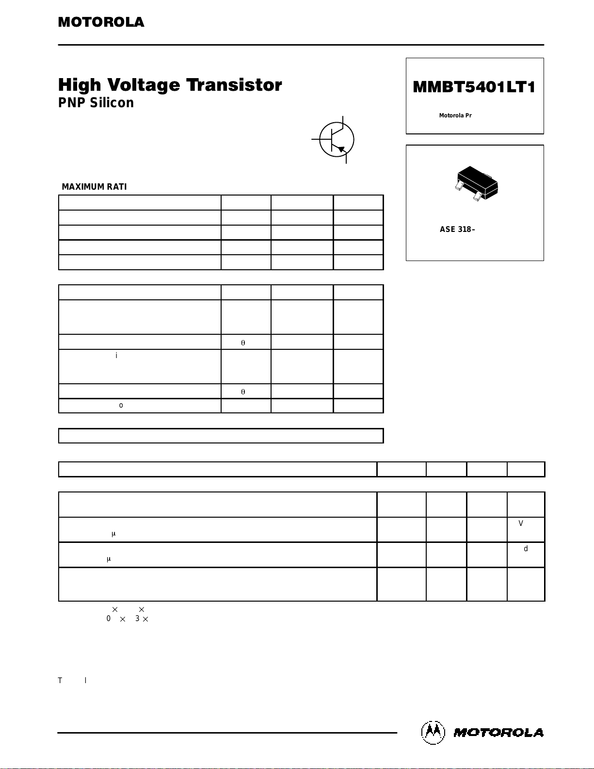
SEMICONDUCTOR TECHNICAL DATA
1
2
3
CASE 318–08, STYLE 6
SOT–23 (TO–236AB)
Motorola Preferred Device
Motorola, Inc. 1996
COLLECTOR
3
1
BASE
2
EMITTER
MMBT5401LT1
2
Motorola Small–Signal Transistors, FETs and Diodes Device Data
ELECTRICAL CHARACTERISTICS
(TA = 25°C unless otherwise noted) (Continued)
Characteristic
Symbol Min Max Unit
ON CHARACTERISTICS
DC Current Gain
(IC = –1.0 mAdc, VCE = –5.0 Vdc)
(IC = –10 mAdc, VCE = –5.0 Vdc)
(IC = –50 mAdc, VCE = –5.0 Vdc)
h
FE
50
60
50
—
240
—
—
Collector–Emitter Saturation Voltage
(IC = –10 mAdc, IB = –1.0 mAdc)
(IC = –50 mAdc, IB = –5.0 mAdc)
V
CE(sat)
—
—
–0.2
–0.5
Vdc
Base–Emitter Saturation Voltage
(IC = –10 mAdc, IB = –1.0 mAdc)
(IC = –50 mAdc, IB = –5.0 mAdc)
V
BE(sat)
—
—
–1.0
–1.0
Vdc
SMALL–SIGNAL CHARACTERISTICS
Current–Gain — Bandwidth Product
(IC = –10 mAdc, VCE = –10 Vdc, f = 100 MHz)
f
T
100 300
MHz
Output Capacitance
(VCB = –10 Vdc, IE = 0, f = 1.0 MHz)
C
obo
— 6.0
pF
Small Signal Current Gain
(IC = –1.0 mAdc, VCE = –10 Vdc, f = 1.0 kHz)
h
fe
40 200
—
Noise Figure
(IC = –200 µAdc, VCE = –5.0 Vdc, RS = 10 Ω, f = 1.0 kHz)
NF
— 8.0
dB
 Loading...