

Motorola MMBT2222AWT1 Datasheet
SEMICONDUCTOR TECHNICAL DATA
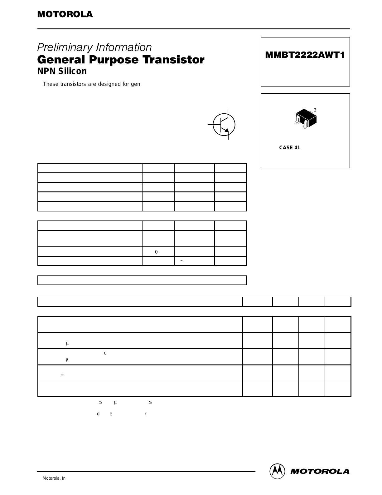
NPN Silicon
These transistors are designed for general purpose amplifier applications. They are housed in the SOT–323/SC–70 package which is
designed for low power surface mount applications.
COLLECTOR
3
Order this document
by MMBT2222AWT1/D
Motorola Preferred Device
3
MAXIMUM RATINGS
Rating Symbol Value Unit
Collector–Emitter Voltage V
Collector–Base Voltage V
Emitter–Base Voltage V
Collector Current — Continuous I
CEO
CBO
EBO
C
THERMAL CHARACTERISTICS
Characteristic Symbol Max Unit
Total Device Dissipation FR–5 Board
TA = 25°C
Thermal Resistance Junction to Ambient
Junction and Storage Temperature TJ, T
P
D
R
q
JA
stg
DEVICE MARKING
MMBT2222AWT1 = 1P
ELECTRICAL CHARACTERISTICS (T
= 25°C unless otherwise noted)
A
Characteristic Symbol Min Max Unit
OFF CHARACTERISTICS
Collector–Emitter Breakdown Voltage
(IC = 1.0 mAdc, IB = 0)
Collector–Base Breakdown Voltage
(IC = 10 mAdc, IE = 0)
Emitter–Base Breakdown Voltage
(IE = 10 mAdc, IC = 0)
Base Cutoff Current
(VCE = 60 Vdc, VEB = 3.0 Vdc)
Collector Cutoff Current
(VCE = 60 Vdc, VEB = 3.0 Vdc)
1. Pulse Test: Pulse Width v 300 ms, Duty Cycle v 2.0%.
(1)
1
BASE
EMITTER
40 Vdc
75 Vdc
6.0 Vdc
600 mAdc
150 mW
833 °C/W
–55 to +150 °C
1
2
2
V
(BR)CEO
V
(BR)CBO
V
(BR)EBO
I
BL
I
CEX
CASE 419–02, STYLE 3
SOT–323/SC–70
40 — Vdc
75 — Vdc
6.0 — Vdc
— 20 nAdc
— 10 nAdc
Thermal Clad is a registered trademark of the Berquist Company.
Preferred devices are Motorola recommended choices for future use and best overall value.
Motorola Small–Signal Transistors, FETs and Diodes Device Data
Motorola, Inc. 1997
1
MMBT2222AWT1
(
CC
,
BE
,
ns
(
CC
,
C
,
ns
ELECTRICAL CHARACTERISTICS (T
ON CHARACTERISTICS
DC Current Gain (1)
(IC = 0.1 mAdc, VCE = 10 Vdc)
(IC = 1.0 mAdc, VCE = 10 Vdc)
(IC = 10 mAdc, VCE = 10 Vdc)
(IC = 150 mAdc, VCE = 10 Vdc)
(IC = 500 mAdc, VCE = 10 Vdc)
Collector–Emitter Saturation Voltage
(IC = 150 mAdc, IB = 15 mAdc)
(IC = 500 mAdc, IB = 50 mAdc)
Base–Emitter Saturation Voltage
(IC = 150 mAdc, IB = 15 mAdc)
(IC = 500 mAdc, IB = 50 mAdc)
(1)
(1)
= 25°C unless otherwise noted) (Continued)
A
Characteristic Symbol Min Max Unit
(1)
SMALL–SIGNAL CHARACTERISTICS
Current–Gain — Bandwidth Product
(IC = 20 mAdc, VCE = 20 Vdc, f = 100 MHz)
Output Capacitance
(VCB = 10 Vdc, IE = 0, f = 1.0 MHz)
Input Capacitance
(VEB = 0.5 Vdc, IC = 0, f = 1.0 MHz)
Input Impedance
(VCE = 10 Vdc, IC = 10 mAdc, f = 1.0 kHz)
Voltage Feedback Ratio
(VCE = 10 Vdc, IC = 10 mAdc, f = 1.0 kHz)
Small–Signal Current Gain
(VCE = 10 Vdc, IC = 10 mAdc, f = 1.0 kHz)
Output Admittance
(VCE = 10 Vdc, IC = 10 mAdc, f = 1.0 kHz)
Noise Figure
(VCE = 10 Vdc, IC = 100 mAdc, RS = 1.0 k ohms, f = 1.0 kHz)
SWITCHING CHARACTERISTICS
Delay Time
Rise Time
Storage Time
Fall Time
1. Pulse Test: Pulse Width v 300 ms, Duty Cycle v 2.0%.
(VCC = 3.0 Vdc, VBE = –0.5 Vdc,
IC = 150 mAdc, IB1 = 15 mAdc)
(VCC = 30 Vdc, IC = 150 mAdc,
IB1 = IB2 = 15 mAdc)
H
FE
V
CE(sat)
V
BE(sat)
f
T
C
obo
C
ibo
h
ie
h
re
h
fe
h
oe
NF — 4.0 dB
t
d
t
r
t
s
t
f
35
50
75
100
40
—
—
0.6
—
300 — MHz
— 8.0 pF
— 30 pF
0.25 1.25 k ohms
— 4.0 X 10
75 375 —
25 200
— 10
— 25
— 225
— 60
—
—
—
—
—
0.3
1.0
1.2
2.0
Vdc
Vdc
m
mhos
—
–4
2
Motorola Small–Signal Transistors, FETs and Diodes Device Data
 Loading...