

Motorola MMBD717LT1 Datasheet
SEMICONDUCTOR TECHNICAL DATA
Order this document
by MMBD717LT1/D
These Schottky barrier diodes are designed for high speed switching applications,
circuit protection, and voltage clamping. Extremely low forward voltage reduces
conduction loss. Miniature surface mount package is excellent for hand held and
portable applications where space is limited.
• Extremely Fast Switching Speed
• Extremely Low Forward Voltage — 0.28 Volts (Typ) @ IF = 1 mAdc
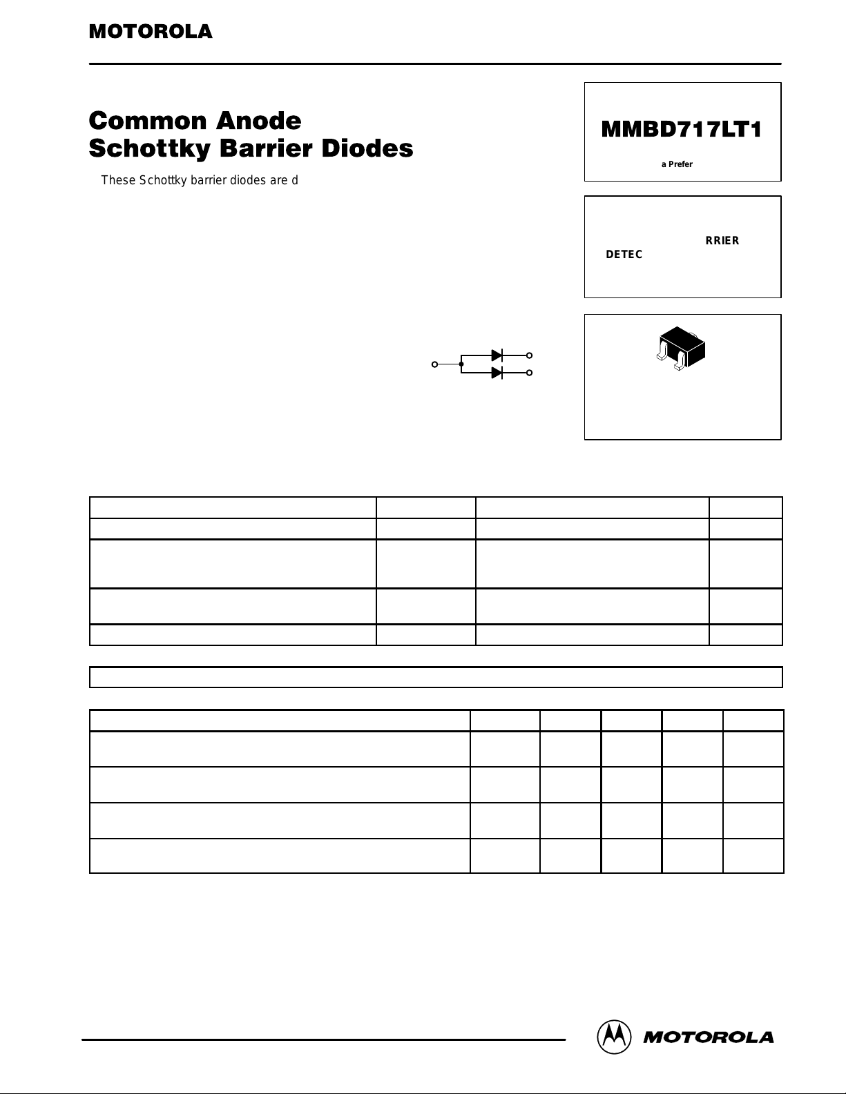
CATHODE
1
2
CATHODE
Symbol Min Typ Max Unit
V
(BR)R
C
T
I
R
V
F
MAXIMUM RATINGS
Reverse Voltage V
Forward Power Dissipation
@ TA = 25°C
Derate above 25°C
Operating Junction
T emperature Range
Storage Temperature Range T
(TJ = 125°C unless otherwise noted)
Rating Symbol Value Unit
DEVICE MARKING
MMBD717LT1 = B3
ELECTRICAL CHARACTERISTICS (T
Characteristic
Reverse Breakdown Voltage
(IR = 10 µA)
Total Capacitance
(VR = 1.0 V, f = 1.0 MHz)
Reverse Leakage
(VR = 10 V)
Forward Voltage
(IF = 1.0 mAdc)
= 25°C unless otherwise noted)
A
ANODE
3
R
P
F
T
J
stg
Motorola Preferred Device
20 VOLT
SCHOTTKY BARRIER
DETECTOR AND SWITCHING
CASE 419–02, STYLE 2
20 Volts
200
1.6
–55 to +150
–55 to +150 °C
20 — — Volts
— 2.0 2.5 pF
— 0.05 1.0 µAdc
— 0.28 0.37 Vdc
DIODES
3
1
2
SOT–323 (SC–70)
mW
mW/°C
°C
Preferred devices are Motorola recommended choices for future use and best overall value.
Thermal Clad is a registered trademark of the Bergquist Company .
REV 3
Motorola, Inc. 1997
5–1Motorola Small–Signal Transistors, FETs and Diodes Device Data
MMBD717LT1
820
Ω
+10 V
0.1 µF
2 k
100
0.1
µ
I
F
µ
H
F
t
t
r
p
10%
t
I
F
t
rr
t
1.0
, FORWARD CURRENT (mA)
F
I
0.1
10
Ω
OUTPUT
50
PULSE
GENERATOR
150°C
125°C
0 0.05
DUT
50 Ω INPUT
SAMPLING
OSCILLOSCOPE
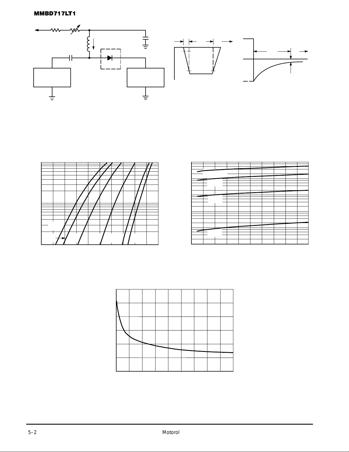
Notes: 1. A 2.0 kΩ variable resistor adjusted for a Forward Current (IF) of 10 mA.
Notes: 2. Input pulse is adjusted so I
Notes: 3. tp » t
rr
V
R(peak)
R
90%
INPUT SIGNAL
is equal to 10 mA.
i
= 1 mA
I
R
(IF = IR = 10 mA; measured
R(REC)
OUTPUT PULSE
at i
R(REC)
= 1 mA)
Figure 1. Recovery Time Equivalent Test Circuit
100
0
TA = 150°C
125°C
85°C
25°C
1.0
2.0 3.0 4.0 5.0 6.0 7.0 8.0 9.0 10
VR, REVERSE VOLTAGE (VOLTS)
85°C
0.1
0.15
VF, FORWARD VOLTAGE (VOLTS)
0.2
25°C
0.25
–40°C
0.3
0.35
–55°C
0.4
0.45
0.5
A)
µ
, REVERSE CURRENT (
R
I
0.001
10
1.0
0.1
0.01
Figure 2. T ypical Forward Voltage Figure 3. Reverse Current versus Reverse
V oltage
5–2
, CAPACITANCE (pF)
T
C
3.0
2.5
2.0
1.5
1.0
0.5
0
0
2.0 4.0
6.0 8.0 10 12 14 16 18
VR, REVERSE VOLTAGE (VOLTS)
Figure 4. T ypical Capacitance
Motorola Small–Signal Transistors, FETs and Diodes Device Data
 Loading...