

Motorola MLD2N06CL Datasheet
1
Motorola TMOS Power MOSFET Transistor Device Data
SMARTDISCRETES
Internally Clamped, Current Limited
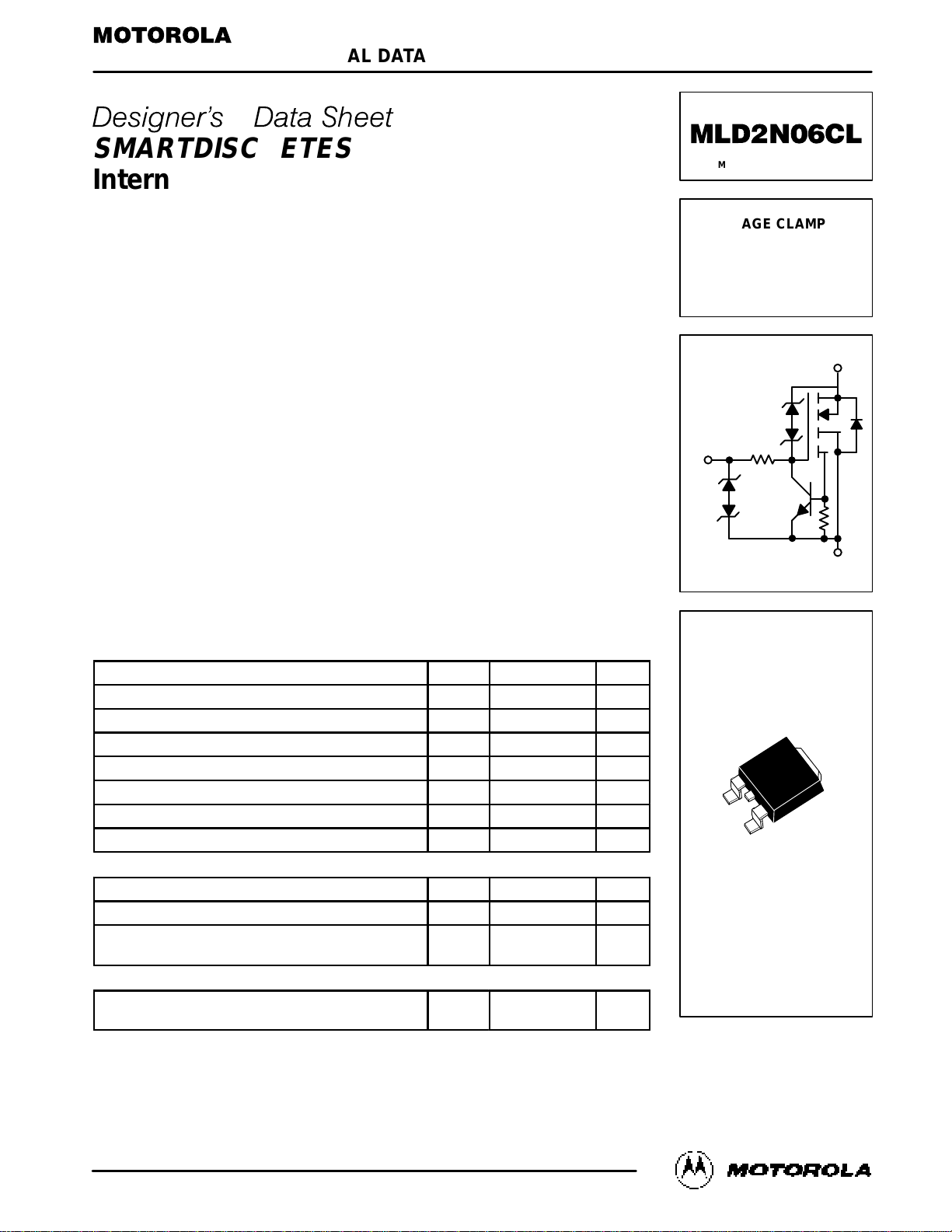
N–Channel Logic Level Power MOSFET
The MLD2N06CL is designed for applications that require a rugged power switching
device with short circuit protection that can be directly interfaced to a microcontrol unit
(MCU). Ideal applications include automotive fuel injector driver, incandescent lamp
driver or other applications where a high in–rush current or a shorted load condition could
occur.
This logic level power MOSFET features current limiting for short circuit protection,
integrated Gate–Source clamping for ESD protection and integral Gate–Drain clamping
for over–voltage protection and Sensefet technology for low on–resistance. No additional
gate series resistance is required when interfacing to the output of a MCU, but a 40 kΩ
gate pulldown resistor is recommended to avoid a floating gate condition.
The internal Gate–Source and Gate–Drain clamps allow the device to be applied
without use of external transient suppression components. The Gate–Source clamp
protects the MOSFET input from e lectrostatic v oltage s tress up t o 2.0 kV. The
Gate–Drain clamp protects the MOSFET drain from the avalanche stress that occurs
with inductive loads. Their unique design provides voltage clamping that is essentially
independent of operating temperature.
The MLD2N06CL is fabricated using Motorola’s SMARTDISCRETES technology which
combines the advantages of a power MOSFET output device with the on–chip protective
circuitry that can be obtained from a standard MOSFET process. This approach offers an
economical means of providing protection to power MOSFETs from harsh automotive and
industrial environments. SMARTDISCRETES devices are specified over a wide temperature range from –50°C to 150°C.
MAXIMUM RATINGS
(TJ = 25°C unless otherwise noted)
Rating
Symbol Value Unit
Drain–to–Source Voltage V
DSS
Clamped Vdc
Drain–to–Gate Voltage (RGS = 1.0 MΩ) V
DGR
Clamped Vdc
Gate–to–Source Voltage — Continuous V
GS
±10 Vdc
Drain Current — Continuous @ TC = 25°C I
D
Self–limited Adc
Total Power Dissipation @ TC = 25°C P
D
40 Watts
Electrostatic Voltage ESD 2.0 kV
Operating and Storage Temperature Range TJ, T
stg
–50 to 150 °C
THERMAL CHARACTERISTICS
Maximum Junction Temperature T
J(max)
150 °C
Thermal Resistance – Junction to Case R
θJC
3.12 °C/W
Maximum Lead Temperature for Soldering Purposes,
1/8″ from case for 5 sec.
T
L
260 °C
DRAIN–TO–SOURCE AVALANCHE CHARACTERISTICS
Single Pulse Drain–to–Source Avalanche Energy
(Starting TJ = 25°C, ID = 2.0 A, L = 40 mH)
E
AS
80 mJ
SMARTDISCRETES is a trademark of Motorola, Inc.
Designer’s Data for “Worst Case” Conditions — The Designer’s Data Sheet permits the design of most circuits entirely from the information presented. SOA Limit
curves — representing boundaries on device characteristics— are given to facilitate “worst case” design.
Preferred devices are Motorola recommended choices for future use and best overall value.
Order this document
by MLD2N06CL/D
MOTOROLA
SEMICONDUCTOR TECHNICAL DATA
MLD2N06CL
Motorola Preferred Device
VOLTAGE CLAMPED
CURRENT LIMITING
MOSFET
62 VOLTS (CLAMPED)
R
DS(on)
= 0.4 OHMS
CASE 369A–13, Style 2
DPAK Surface Mount
D
G
S
R1
R2
Motorola, Inc. 1996
MLD2N06CL
2
Motorola TMOS Power MOSFET Transistor Device Data
ELECTRICAL CHARACTERISTICS
(TC = 25°C unless otherwise noted)
Characteristic
Symbol Min Typ Max Unit
OFF CHARACTERISTICS
Drain–to–Source Breakdown Voltage
(ID = 20 mAdc, VGS = 0 Vdc)
(ID = 20 mAdc, VGS = 0 Vdc, TJ = 150°C)
V
(BR)DSS
58
58
62
62
66
66
Vdc
Zero Gate Voltage Drain Current
(VDS = 40 Vdc, VGS = 0 Vdc)
(VDS = 40 Vdc, VGS = 0 Vdc, TJ = 150°C)
I
DSS
—
—
0.6
6.0
5.0
20
µAdc
Gate–Source Leakage Current
(VG = 5.0 Vdc, VDS = 0 Vdc)
(VG = 5.0 Vdc, VDS = 0 Vdc, TJ = 150°C)
I
GSS
—
—
0.5
1.0
5.0
20
µAdc
ON CHARACTERISTICS(1)
Gate Threshold Voltage
(ID = 250 µAdc, VDS = VGS)
(ID = 250 µAdc, VDS = VGS, TJ = 150°C)
V
GS(th)
1.0
0.6
1.5
1
2.0
1.6
Vdc
Static Drain Current Limit
(VGS = 5.0 Vdc, VDS = 10 Vdc)
(VGS = 5.0 Vdc, VDS = 10 Vdc, TJ = 150°C)
I
D(lim)
3.8
1.6
4.4
2.4
5.2
2.9
Adc
Static Drain–to–Source On–Resistance
(ID = 1.0 Adc, VGS = 5.0 Vdc)
(ID = 1.0 Adc, VGS = 5.0 Vdc, TJ = 150°C)
R
DS(on)
—
—
0.3
0.53
0.4
0.7
Ohms
Forward Transconductance (ID = 1.0 Adc, VDS = 10 Vdc) g
FS
1.0 1.4 — mhos
Static Source–to–Drain Diode Voltage
(IS = 1.0 Adc, VGS = 0 Vdc)
V
SD
— 1.1 1.5
Vdc
SWITCHING CHARACTERISTICS(2)
Turn–On Delay Time
t
d(on)
— 1.0 1.5
µs
Rise Time
DD
= 30 Vdc, ID = 1.0 Adc,
t
r
— 3.0 5.0
Turn–Off Delay Time
(VDD = 30 Vdc, ID = 1.0 Adc,
V
GS(on)
= 5.0 Vdc, RGS = 25 Ohms)
t
d(off)
— 5.0 8.0
Fall Time t
f
— 3.0 5.0
(1) Pulse Test: Pulse Width ≤ 300 µs, Duty Cycle ≤ 2%.
(2) Switching characteristics are independent of operating junction temperature.
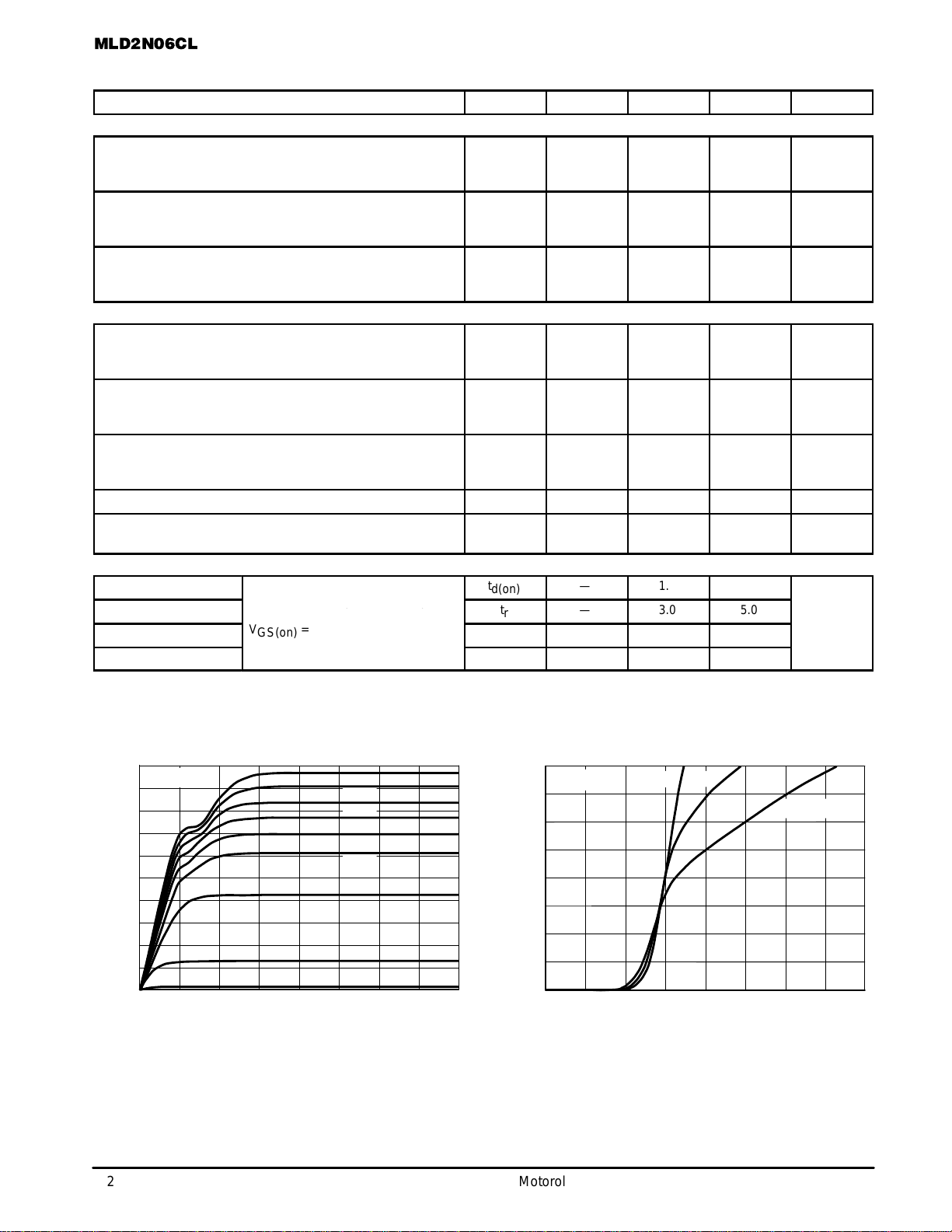
VDS, DRAIN–TO–SOURCE VOLTAGE (VOLTS)
I
D
, DRAIN CURRENT (AMPS)
I
D
, DRAIN CURRENT (AMPS)
VGS, GATE–TO–SOURCE VOLTAGE (VOLTS)
TJ = 25
°C
VDS ≥ 7.5 V
TJ = 150
°C
25
°C
–55
°C
0 1 2 3 8
2.5
2.0
1.5
1.0
0.5
0
3.0
3.5
4.0
4 5 6 7
0 2 4 6 8
5
4
3
2
1
0
6.0 V
5.5 V
5.0 V
4.5 V
4.0 V
3.5 V
3.0 V
2.5 V
2.0 V
(V
Figure 1. Output Characteristics Figure 2. Transfer Function
 Loading...