

Motorola MJ10012, MJH10012 Datasheet
1
Motorola Bipolar Power Transistor Device Data
The MJ10012 and MJH10012 are high–voltage, high–current Darlington transistors
designed for automotive ignition, switching regulator and motor control applications.
• Collector–Emitter Sustaining Voltage —
V
CEO(sus)
= 400 Vdc (Min)
• 175 Watts Capability at 50 Volts
• Automotive Functional Tests
MAXIMUM RATINGS
Rating
Symbol
MJ10012
MJH10012
Unit
Collector–Emitter Voltage
V
CEO
400
Vdc
Collector–Emitter Voltage
(RBE = 27 Ω)
V
CER
550
Vdc
Collector–Base Voltage
V
CBO
600
Vdc
Emitter–Base Voltage
V
EBO
8.0
Vdc
Collector Current — Continuous
— Peak (1)
I
C
10
15
Adc
Base Current
I
B
2.0
Adc
Total Power Dissipation
@ TC = 25_C
@ TC = 100_C
Derate above 25_C
P
D
175
100
1.0
118
47.5
1.05
Watts
Watts
W/_C
Operating and Storage Junction
Temperature Range
TJ, T
stg
–65 to +200
–55 to +150
_
C
THERMAL CHARACTERISTICS
Characteristic
Symbol
Max
Unit
Thermal Resistance, Junction to Case
R
θJC
1.0
0.95
_
C/W
Maximum Lead Temperature for
Soldering Purposes: 1/8″ from
Case for 5 Seconds
T
L
275
275
_
C
(1) Pulse Test: Pulse Width = 5.0 ms, Duty Cycle v 10%.
SEMICONDUCTOR TECHNICAL DATA
Order this document
by MJ10012/D
Motorola, Inc. 1995
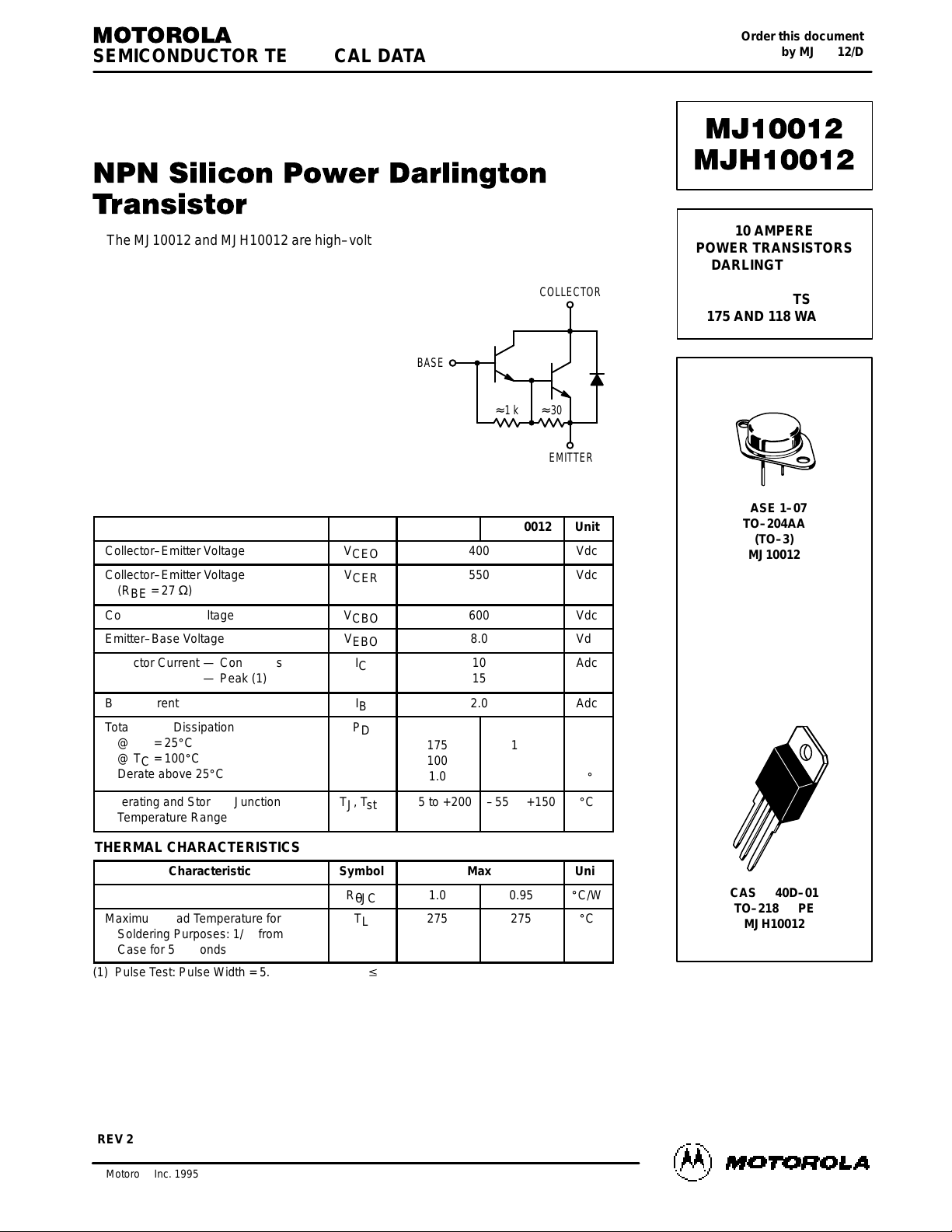
10 AMPERE
POWER TRANSISTORS
DARLINGTON NPN
SILICON
400 VOLTS
175 AND 118 WATTS
CASE 1–07
TO–204AA
(TO–3)
MJ10012
CASE 340D–01
TO–218 TYPE
MJH10012
≈
1 k≈ 30
EMITTER
BASE
COLLECTOR
REV 2
2
Motorola Bipolar Power Transistor Device Data
ELECTRICAL CHARACTERISTICS (T
C
= 25_C unless otherwise noted)
Characteristic
Symbol
Min
Typ
Max
Unit
OFF CHARACTERISTICS (1)
Collector–Emitter Sustaining Voltage (Figure 1)
(IC = 200 mAdc, IB = 0, V
clamp
= Rated V
CEO
)
V
CEO(sus)
400
—
—
Vdc
Collector–Emitter Sustaining Voltage (Figure 1)
(IC = 200 mAdc, RBE = 27 Ohms, V
clamp
= Rated V
CER
)
V
CER(sus)
425
—
—
Vdc
Collector Cutoff Current (Rated V
CER
, RBE = 27 Ohms)
I
CER
—
—
1.0
mAdc
Collector Cutoff Current (Rated V
CBO
, IE = 0)
I
CBO
—
—
1.0
mAdc
Emitter Cutoff Current (VEB = 6.0 Vdc, IC = 0)
I
EBO
—
—
40
mAdc
ON CHARACTERISTICS (1)
DC Current Gain
(IC = 3.0 Adc, VCE = 6 0 Vdc)
(IC = 6.0 Adc, VCE = 6.0 Vdc)
(IC = 10 Adc, VCE = 6.0 Vdc)
h
FE
300
100
20
550
350
150
—
2000
—
—
Collector–Emitter Saturation Voltage
(IC = 3.0 Adc, IB = 0.6 Adc)
(IC = 6.0 Adc, IB = 0.6 Adc)
(IC = 10 Adc, IB = 2.0 Adc)
V
CE(sat)
—
—
—
—
—
—
1 5
2.0
2.5
Vdc
Base Emitter Saturation Voltage
(IC = 6.0 Adc, IB = 0.6 Adc)
(IC = 10 Adc, IB = 2.0 Adc)
V
BE(sat)
—
—
—
—
2.5
3.0
Vdc
Base Emitter On Voltage (IC = 10 Adc, VCE = 6.0 Vdc)
V
BE(on)
—
—
2.8
Vdc
Diode Forward Voltage (IF = 10 Adc)
V
f
—
2.0
3.5
Vdc
DYNAMIC CHARACTERISTICS
Output Capacitance (VCB = 10 Vdc, IE = 0, f
test
= 100 kHz)
C
ob
—
165
350
pF
SWITCHING CHARACTERISTICS
Storage Time
CC
= 12 Vdc, IC = 6.0 Adc,
t
s
—
7 5
15
µs
Fall Time
(VCC = 12 Vdc, IC = 6.0 Adc,
IB1 = IB2 = 0.3 Adc) Figure 2
t
f
—
5.2
15
µs
FUNCTIONAL TESTS
Second Breakdown Collector Current with
Base–Forward Biased
I
S/B
See Figure 10
—
Pulsed Energy Test (See Figure 12)
IC2L/2
—
—
180
mJ
(1) Pulse Test: Pulse Width = 300 µs, Duty Cycle = 2%.
VCC [ 14 V
ADJUST UNTIL IC = 6 A
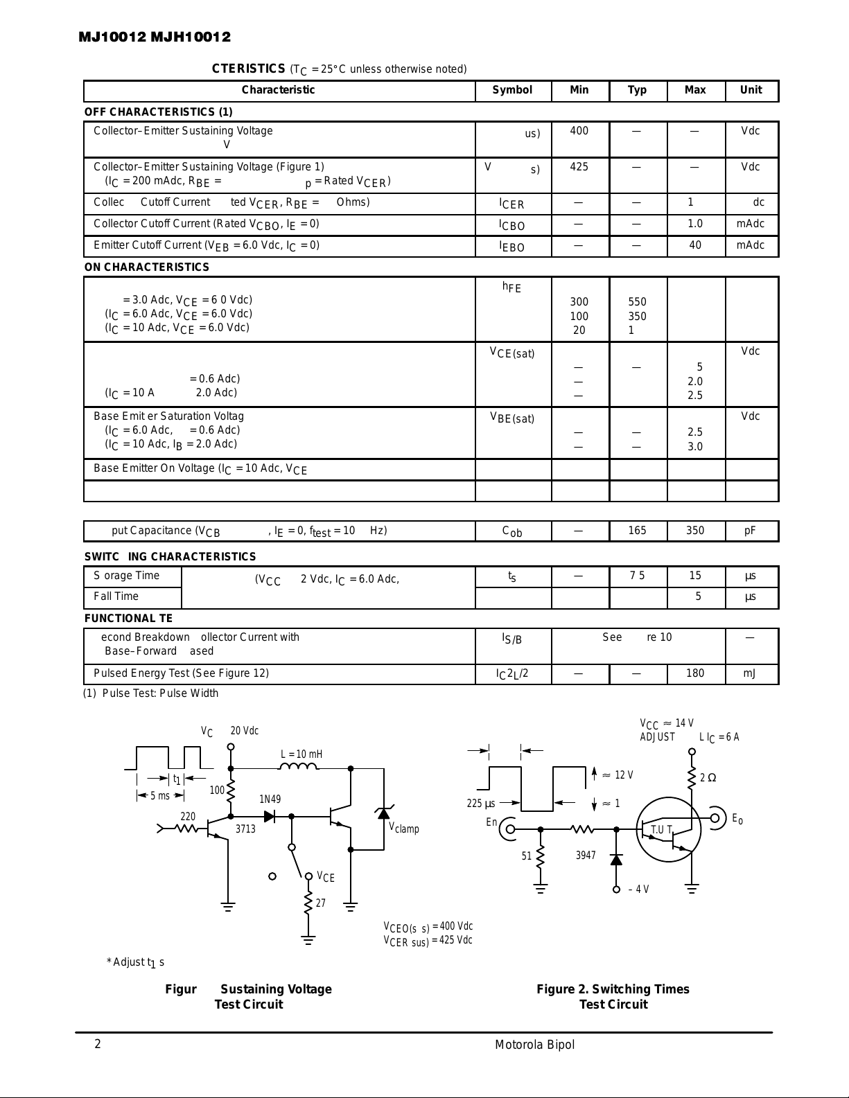
V
CEO(sus)
= 400 Vdc
V
CER(sus)
= 425 Vdc
VCC = 20 Vdc
Figure 1. Sustaining Voltage
Test Circuit
Figure 2. Switching Times
Test Circuit
*Adjust t1 such that IC reaches 200 mA at VCE = V
clamp
0 V
*
t
1
5 ms
220
100
1N4933
2N3713
L = 10 mH
V
CER
27
V
clamp
2
Ω
E
o
T.U.T.
– 4 V
[
12 V
En
51
1N3947
225 µs
[
12 V
0
(V
10 V
V
CEO
V
clamp
25
µ
s
 Loading...