

Motorola MJF6107 Datasheet
1
Motorola Bipolar Power Transistor Device Data
For Isolated Package Applications
Designed for general–purpose amplifier and switching applications, where the
mounting surface of the device is required to be electrically isolated from the heatsink
or chassis.
• Electrically Similar to the Popular 2N6107
• 70 V
CEO(sus)
• 7 A Rated Collector Current
• No Isolating Washers Required
• Reduced System Cost
• High Current Gain–Bandwidth Product
fT = 4 MHz (Min) Ca, IC = 500 mAdc
• UL Recognized, File #E69369, to 3500 V
RMS
Isolation
MAXIMUM RATINGS
Rating
Symbol
Value
ÎÎÎ
ÎÎÎ
ÎÎÎ
Unit
Collector–Emitter Voltage
V
CEO
70
ÎÎÎ
ÎÎÎ
ÎÎÎ
Vdc
Collector–Base Voltage
V
CB
80
ÎÎÎ
ÎÎÎ
ÎÎÎ
Vdc
Emitter–Base Voltage
V
EB
5
ÎÎÎ
ÎÎÎ
ÎÎÎ
Vdc
RMS Isolation Voltage (1) Test No. 1 Per Fig. 13
(for 1 sec, R.H. < 30%, Test No. 2 Per Fig. 14
TA = 25_C) Test No. 3 Per Fig. 15
V
ISOL
4500
3500
1500
ÎÎÎ
ÎÎÎ
ÎÎÎ
ÎÎÎ
V
RMS
Collector Current — Continuous
Peak
I
C
7
10
ÎÎÎ
ÎÎÎ
ÎÎÎ
ÎÎÎ
Adc
Base Current
I
B
3
ÎÎÎ
ÎÎÎ
ÎÎÎ
Adc
Total Power Dissipation* @ TC = 25_C
Derate above 25_C
P
D
34
0.27
ÎÎÎ
ÎÎÎ
ÎÎÎ
ÎÎÎ
Watts
W/_C
Total Power Dissipation @ TA = 25_C
Derate above 25_C
P
D
2
0.016
ÎÎÎ
ÎÎÎ
ÎÎÎ
Watts
W/_C
Operating and Storage Junction Temperature Range
TJ, T
stg
–65 to +150
ÎÎÎ
ÎÎÎ
ÎÎÎ
_
C
THERMAL CHARACTERISTICS
Characteristic
Symbol
Max
ÎÎÎ
ÎÎÎ
ÎÎÎ
Unit
Thermal Resistance, Junction to Ambient
R
θJA
62.5
ÎÎÎ
ÎÎÎ
ÎÎÎ
_
C/W
Thermal Resistance, Junction to Case*
R
θJC
3.7
ÎÎÎ
ÎÎÎ
ÎÎÎ
_
C/W
Lead Temperature for Soldering Purpose
T
L
260
ÎÎÎ
ÎÎÎ
ÎÎÎ
_
C
*Measurement made with thermocouple contacting the bottom insulated mounting surface (in a location beneath the die), the device mounted on
a heatsink with thermal grease and a mounting torque of ≥ 6 in. lbs.
(1) Proper strike and creepage distance must be provided.
SEMICONDUCTOR TECHNICAL DATA
Order this document
by MJF6107/D
Motorola, Inc. 1995
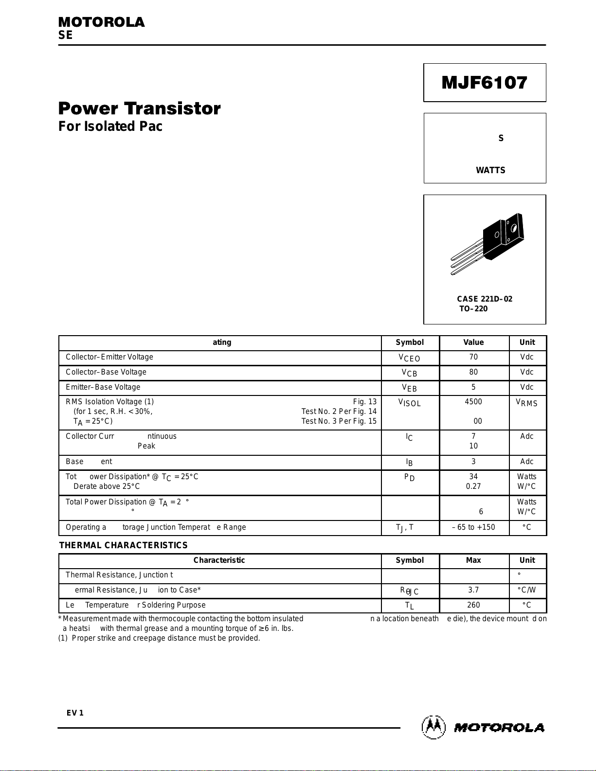
PNP SILICON
POWER TRANSISTOR
7 AMPERES
70 VOLTS
34 WATTS
CASE 221D–02
TO–220 TYPE
REV 1
MJF6107
2
Motorola Bipolar Power Transistor Device Data
ELECTRICAL CHARACTERISTICS (T
C
= 25_C unless otherwise noted)
Characteristic
ÎÎÎÎ
ÎÎÎÎ
ÎÎÎÎ
Symbol
Min
Max
ÎÎÎ
ÎÎÎ
ÎÎÎ
Unit
OFF CHARACTERISTICS
Collector–Emitter Sustaining Voltage (1) (IC = 100 mAdc, IB = 0)
ÎÎÎÎ
ÎÎÎÎ
ÎÎÎÎ
V
CEO(sus)
70
—
ÎÎÎ
ÎÎÎ
ÎÎÎ
Vdc
Collector Cutoff Current (VCE = 80 Vdc, IB = 0)
ÎÎÎÎ
ÎÎÎÎ
ÎÎÎÎ
I
CES
—
1
ÎÎÎ
ÎÎÎ
ÎÎÎ
µAdc
Collector Cutoff Current (VCE = 80 Vdc, V
EB(off)
= 1.5 Vdc)
ÎÎÎÎ
ÎÎÎÎ
ÎÎÎÎ
I
CEX
—
1
ÎÎÎ
ÎÎÎ
ÎÎÎ
µAdc
Emitter Cutoff Current (VBE = 5 Vdc, IC = 0)
ÎÎÎÎ
ÎÎÎÎ
ÎÎÎÎ
I
EBO
—
1
ÎÎÎ
ÎÎÎ
ÎÎÎ
µAdc
ON CHARACTERISTICS (1)
DC Current Gain (IC = 2 Adc, VCE = 4 Vdc)
DC Current Gain (IC = 7 Adc, VCE = 4 Vdc)
ÎÎÎÎ
ÎÎÎÎ
ÎÎÎÎ
ÎÎÎÎ
h
FE
30
5
90
—
ÎÎÎ
ÎÎÎ
ÎÎÎ
ÎÎÎ
—
Collector–Emitter Saturation Voltage (IC = 7 Adc, IB = 3 Adc)
ÎÎÎÎ
ÎÎÎÎ
ÎÎÎÎ
V
CE(sat)
—
2
ÎÎÎ
ÎÎÎ
ÎÎÎ
Vdc
Base–Emitter On Voltage (IC = 7 Adc, VCE = 4 Vdc)
ÎÎÎÎ
ÎÎÎÎ
ÎÎÎÎ
V
BE(on)
—
2
ÎÎÎ
ÎÎÎ
ÎÎÎ
Vdc
DYNAMIC CHARACTERISTICS
Current Gain–Bandwidth Product (2)
(IC = 500 mAdc, VCE = 4 Vdc, f
test
= 1 MHz)
ÎÎÎÎ
ÎÎÎÎ
ÎÎÎÎ
f
T
4
—
ÎÎÎ
ÎÎÎ
ÎÎÎ
MHz
Output Capacitance (VCB = 10 Vdc, IE = 0, f = 1 MHz)
ÎÎÎÎ
ÎÎÎÎ
ÎÎÎÎ
C
ob
—
250
ÎÎÎ
ÎÎÎ
ÎÎÎ
pF
Small–Signal Current Gain (IC = 0.5 Adc, VCE = 4 Vdc, f = 50 kHz)
ÎÎÎÎ
ÎÎÎÎ
ÎÎÎÎ
h
fe
20
—
ÎÎÎ
ÎÎÎ
ÎÎÎ
—
NOTES:
1. Pulse Test: Pulse Width v 300 µs, Duty Cycle v 2%.
2. fT = |h
fe|
• f
test
.
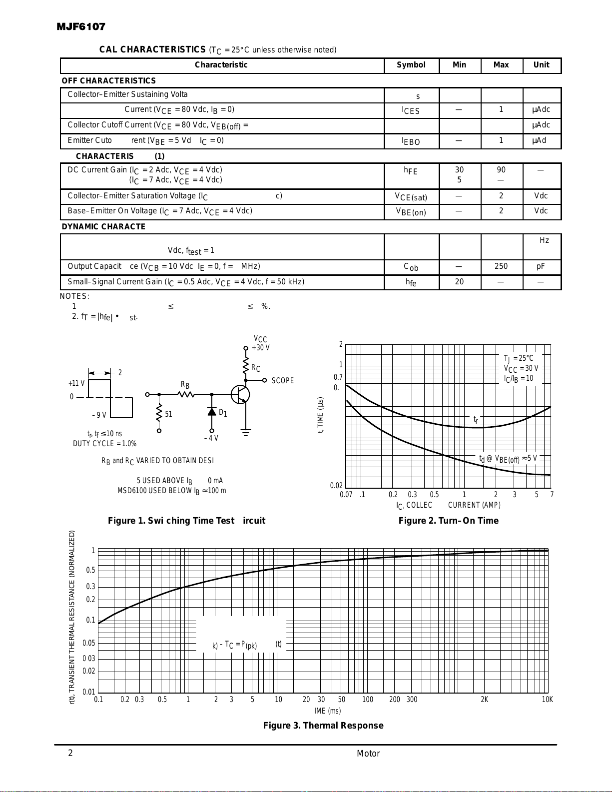
Figure 1. Switching Time Test Circuit
+11 V
25 µs
0
–9 V
R
B
–4 V
D
1
SCOPE
V
CC
+30 V
R
C
tr, tf
≤
10 ns
DUTY CYCLE = 1.0%
51
RB and RC VARIED TO OBTAIN DESIRED CURRENT LEVELS
D1 MUST BE FAST RECOVERY TYPE, e.g.:
1N5825 USED ABOVE IB
≈
100 mA
MSD6100 USED BELOW IB
≈
100 mA
t, TIME ( s)
µ
t, TIME (ms)
1
0.01
0.3
0.2
0.1
0.05
0.02
r(t), TRANSIENT THERMAL RESISTANCE (NORMALIZED)
0.5 10 30 50 100 300 500 1K 3K 5K
SINGLE PULSE
R
θ
JC(t)
= r(t) R
θ
JC
T
J(pk)
– TC = P
(pk)
R
θ
JC
(t)
1 53 10K
0.5
0.3
0.03
0.1 0.2 20 200 2K2
0.1
IC, COLLECTOR CURRENT (AMP)
0.3 3
2
TJ = 25°C
VCC = 30 V
IC/IB = 10
td @ V
BE(off)
≈ 5 V
t
r
0.07 0.2 0.5 1 2 5 7
Figure 2. Turn–On Time
Figure 3. Thermal Response
1
0.7
0.5
0.3
0.2
0.1
0.07
0.05
0.03
0.02
 Loading...