

Motorola MJF18009, MJE18009 Datasheet

1
Motorola Bipolar Power Transistor Device Data
!
The MJE/MJF18009 has an application specific state–of–the–art die designed for
use in 220 V line–operated Switchmode Power supplies and electronic ballast (“light
ballast”). These high voltage/high speed transistors exhibit the following main
features:
• Improved Efficiency Due to Low Base Drive Requirements:
— High and Flat DC Current Gain h
FE
— Fast Switching
— No Coil Required in Base Circuit for Turn–Off (No Current Tail)
• Full Characterization at 125_C
• Motorola “6 SIGMA” Philosophy Provides Tight and Reproducible Parametric
Distributions
• Specified Dynamic Saturation Data
• Two Package Choices: Standard TO–220 or Isolated TO–220
MAXIMUM RATINGS
Rating
Symbol
MJE18009
MJF18009
Unit
Collector–Emitter Sustaining Voltage
V
CEO
450
Vdc
Collector–Emitter Breakdown Voltage
V
CES
1000
Vdc
Collector–Base Breakdown Voltage
V
CBO
1000
Vdc
Emitter–Base Voltage
V
EBO
9
Vdc
Collector Current — Continuous
— Peak (1)
I
C
I
CM
10
20
Adc
Base Current — Continuous
— Peak (1)
I
B
I
BM
4
8
Adc
*Total Device Dissipation @ TC = 25°C
*Derate above 25_C
P
D
150
1.2
50
0.4
Watt
W/_C
Operating and Storage Temperature
TJ, T
stg
–65 to 150
_
C
RMS Isolation Voltage (2) Per Figure 22
(1s, 25°C, Humidity ≤ 30%) Per Figure 23
TC = 25°C Per Figure 24
V
ISOL1
V
ISOL2
V
ISOL3
4500
3500
1500
V
THERMAL CHARACTERISTICS
Rating
Symbol
MJE18009
MJF18009
Unit
Thermal Resistance — Junction to Case
— Junction to Ambient
R
θJC
R
θJA
0.83
62.5
2.5
62.5
_
C/W
Maximum Lead Temperature for Soldering
Purposes: 1/8″ from Case for 5 Seconds
T
L
260
_
C
(1) Pulse Test: Pulse Width = 5 ms, Duty Cycle v 10%.
(2) Proper strike and creepage distance must be provided.
Designer’s Data for “Worst Case” Conditions — The Designer’s Data Sheet permits the design of most circuits entirely from the information presented. SOA Limit
curves — representing boundaries on device characteristics — are given to facilitate “worst case” design.
Designer’s and SWITCHMODE are trademarks of Motorola, Inc.
SEMICONDUCTOR TECHNICAL DATA
Order this document
by MJE18009/D
Motorola, Inc. 1995
POWER TRANSISTORS
10 AMPERES
1000 VOLTS
50 and 150 WATTS
CASE 221A–06
TO–220AB
CASE 221D–02
TO–220 FULLPACK
2
Motorola Bipolar Power Transistor Device Data
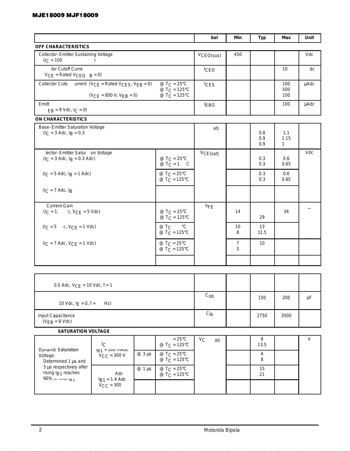
ELECTRICAL CHARACTERISTICS
(T
C
= 25°C unless otherwise noted)
Characteristic
Symbol
Min
Typ
Max
Unit
OFF CHARACTERISTICS
Collector–Emitter Sustaining Voltage
(IC = 100 mA, L = 25 mH)
V
CEO(sus)
450
Vdc
Collector Cutoff Current
(VCE = Rated V
CEO
, IB = 0)
I
CEO
100
µAdc
Collector Cutoff Current (VCE = Rated V
CES
, VEB = 0)
Collector Cutoff Current (VCE = 800 V, VEB = 0)
@ TC = 25°C
@ TC = 125°C
@ TC = 125°C
I
CES
100
500
100
µAdc
Emitter–Cutoff Current
(VEB = 9 Vdc, IC = 0)
I
EBO
100
µAdc
ON CHARACTERISTICS
Base–Emitter Saturation Voltage
(IC = 3 Adc, IB = 0.3 Adc)
(IC = 5 Adc, IB = 1 Adc)
(IC = 7 Adc, IB = 1.4 Adc)
V
BE(sat)
0.8
0.9
0.9
1.1
1.15
1.25
Vdc
Collector–Emitter Saturation Voltage
(IC = 3 Adc, IB = 0.3 Adc)
@ TC = 25°C
@ TC = 125°C
0.3
0.3
0.6
0.65
(IC = 5 Adc, IB = 1 Adc)
@ TC = 25°C
@ TC = 125°C
0.3
0.3
0.6
0.65
(IC = 7 Adc, IB = 1.4 Adc)
@ TC = 25°C
@ TC = 125°C
0.35
0.4
0.7
0.9
DC Current Gain
(IC = 1.5 Adc, VCE = 5 Vdc)
@ TC = 25°C
@ TC = 125°C
14
29
34
(IC = 5 Adc, VCE = 1 Vdc)
@ TC = 25°C
@ TC = 125°C
10
8
13
11.5
(IC = 7 Adc, VCE = 1 Vdc)
@ TC = 25°C
@ TC = 125°C
7
5
10
7.5
—
(IC = 10 mAdc, VCE = 5 Vdc)
@ TC = 25°C
10
25
—
DYNAMIC CHARACTERISTICS
Current Gain Bandwidth
(IC = 0.5 Adc, VCE = 10 Vdc, f = 1 MHz)
f
T
12
MHz
Output Capacitance
(VCB = 10 Vdc, IE = 0, f = 1 MHz)
C
ob
150
200
pF
Input Capacitance
(VEB = 8 Vdc)
C
ib
2750
3500
pF
DYNAMIC SATURATION VOLTAGE
@ 1 µs
@ TC = 25°C
@ TC = 125°C
8
13.5
Dynamic Saturation
Voltage:
Determined 1 µs and
IB1 = 300 mAdc
VCC = 300 V
@ 3 µs
@ TC = 25°C
@ TC = 125°C
4
8
µs and
3 µs respectively after
rising IB1 reaches
@ 1 µs
@ TC = 25°C
@ TC = 125°C
15
21
90% of final I
B1
IB1 = 1.4 Adc
VCC = 300 V
@ 3 µs
@ TC = 25°C
@ TC = 125°C
2
2.7
V
CE(sat)
Vdc
IC = 3 Adc
IC = 7 Adc
h
FE
V
CE(dsat)
—
V

3
Motorola Bipolar Power Transistor Device Data
ELECTRICAL CHARACTERISTICS (T
C
= 25°C unless otherwise noted)
Characteristic
Symbol
Min
Typ
Max
Unit
SWITCHING CHARACTERISTICS: Resistive Load (D.C. ≤ 10%, Pulse Width = 20 µs)
Turn–on Time
@ TC = 25°C
@ TC = 125°C
t
on
220
220
300
ns
Turn–off Time
IB2 = 1.5 Adc
VCC = 300 Vdc
@ TC = 25°C
@ TC = 125°C
t
off
1.28
1.6
2.5
µs
Turn–on Time
@ TC = 25°C
@ TC = 125°C
t
on
120
350
250
ns
Turn–off Time
IB2 = 2.5 Adc
VCC = 300 Vdc
@ TC = 25°C
@ TC = 125°C
t
off
2.2
2.6
2.5
µs
Turn–on Time
@ TC = 25°C
@ TC = 125°C
t
on
175
500
300
ns
Turn–off Time
IB2 = 3.5 Adc
VCC = 300 Vdc
@ TC = 25°C
@ TC = 125°C
t
off
1.75
2.1
2.5
µs
SWITCHING CHARACTERISTICS: Inductive Load (V
clamp
= 300 V, VCC = 15 V, L = 200 µH)
Fall Time
@ TC = 25°C
@ TC = 125°C
t
f
110
125
200
ns
Storage Time
IC = 3 Adc
IB1 = 0.3 Adc
I
= 1.5 Adc
@ TC = 25°C
@ TC = 125°C
t
s
2
2.6
2.75
µs
Crossover Time
IB2 = 1.5 Adc
@ TC = 25°C
@ TC = 125°C
t
c
250
300
350
ns
Fall Time
@ TC = 25°C
@ TC = 125°C
t
f
110
135
200
ns
Storage Time
IC = 5 Adc
IB1 = 1 Adc
I
= 2.5 Adc
@ TC = 25°C
@ TC = 125°C
t
s
2.4
3.1
3.5
µs
Crossover Time
IB2 = 2.5 Adc
@ TC = 25°C
@ TC = 125°C
t
c
260
300
350
ns
Fall Time
@ TC = 25°C
@ TC = 125°C
t
f
105
150
200
ns
Storage Time
IC = 7 Adc
IB1 = 1.4 Adc
I
= 3.5 Adc
@ TC = 25°C
@ TC = 125°C
t
s
1.75
2.25
2.75
µs
Crossover Time
IB2 = 3.5 Adc
@ TC = 25°C
@ TC = 125°C
t
c
225
300
350
ns
IC = 3 Adc, IB1 = 0.3 Adc
IC = 5 Adc, IB1 = 1 Adc
IC = 7 Adc, IB1 = 1.4 Adc
 Loading...