

Motorola MJF18008, MJE18008 Datasheet
1
Motorola Bipolar Power Transistor Device Data
SWITCHMODE
NPN Bipolar Power Transistor
For Switching Power Supply Applications
The MJE/MJF18008 have an applications specific state–of–the–art die designed
for use in 220 V line–operated Switchmode Power supplies and electronic light
ballasts. These high voltage/high speed transistors offer the following:
• Improved Efficiency Due to Low Base Drive Requirements:
— High and Flat DC Current Gain h
FE
— Fast Switching
— No Coil Required in Base Circuit for Turn–Off (No Current Tail)
• Tight Parametric Distributions are Consistent Lot–to–Lot
• Two Package Choices: Standard TO–220 or Isolated TO–220
• MJF18008, Case 221D, is UL Recognized at 3500 V
RMS
: File #E69369
MAXIMUM RATINGS
Rating
Symbol
MJE18008
MJF18008
Unit
Collector–Emitter Sustaining Voltage
V
CEO
450
Vdc
Collector–Emitter Breakdown Voltage
V
CES
1000
Vdc
Emitter–Base Voltage
V
EBO
9.0
Vdc
Collector Current — Continuous
— Peak(1)
I
C
I
CM
8.0
16
Adc
Base Current — Continuous
— Peak(1)
I
B
I
BM
4.0
8.0
Adc
RMS Isolation Voltage(2) Test No. 1 Per Fig. 22a
(for 1 sec, R.H. < 30%, Test No. 1 Per Fig. 22b
TC = 25_C) Test No. 1 Per Fig. 22c
V
ISOL
—
—
—
4500
3500
1500
Volts
Total Device Dissipation (TC = 25°C)
Derate above 25_C
P
D
125
1.0
45
0.36
Watts
W/_C
Operating and Storage Temperature
TJ, T
stg
–65 to 150
_
C
THERMAL CHARACTERISTICS
Rating
Symbol
MJE18008
MJF18008
Unit
Thermal Resistance — Junction to Case
— Junction to Ambient
R
θJC
R
θJA
1.0
62.5
2.78
62.5
_
C/W
Maximum Lead Temperature for Soldering
Purposes: 1/8″ from Case for 5 Seconds
T
L
260
_
C
ELECTRICAL CHARACTERISTICS (T
C
= 25_C unless otherwise specified)
Characteristic
Symbol
Min
Typ
Max
ÎÎÎ
ÎÎÎ
ÎÎÎ
Unit
OFF CHARACTERISTICS
Collector–Emitter Sustaining Voltage (IC = 100 mA, L = 25 mH)
V
CEO(sus)
450
—
—
ÎÎÎ
ÎÎÎ
ÎÎÎ
Vdc
Collector Cutoff Current (VCE = Rated V
CEO
, IB = 0)
I
CEO
—
—
100
ÎÎÎ
ÎÎÎ
µAdc
Collector Cutoff Current (VCE = Rated V
CES
, VEB = 0)
(TC = 125_C)
Collector Cutoff Current (VCE = 800 V, VEB = 0) (TC = 125_C)
I
CES
—
—
—
—
—
—
100
500
100
ÎÎÎ
ÎÎÎ
ÎÎÎ
ÎÎÎ
ÎÎÎ
µAdc
Emitter Cutoff Current (VEB = 9.0 Vdc, IC = 0)
I
EBO
—
—
100
ÎÎÎ
ÎÎÎ
ÎÎÎ
µAdc
(1) Pulse Test: Pulse Width = 5.0 ms, Duty Cycle v 10%. (continued)
(2) Proper strike and creepage distance must be provided.
Designer’s Data for “Worst Case” Conditions — The Designer’s Data Sheet permits the design of most circuits entirely from the information presented. SOA Limit
curves — representing boundaries on device characteristics — are given to facilitate “worst case” design.
Preferred devices are Motorola recommended choices for future use and best overall value.
Designer’s and SWITCHMODE are trademarks of Motorola, Inc.
MOTOROLA
SEMICONDUCTOR TECHNICAL DATA
Order this document
by MJE18008/D
Motorola, Inc. 1995
MJE18008
MJF18008
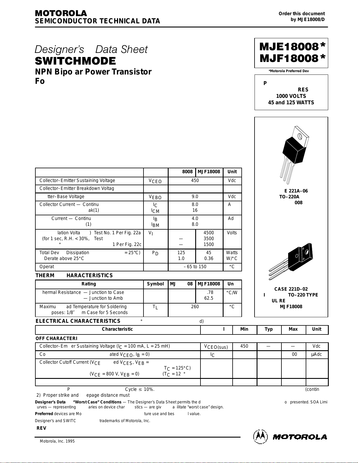
POWER TRANSISTOR
8.0 AMPERES
1000 VOLTS
45 and 125 WATTS
*Motorola Preferred Device
*
*
CASE 221A–06
TO–220AB
MJE18008
CASE 221D–02
ISOLATED TO–220 TYPE
UL RECOGNIZED
MJF18008
REV 1
2
Motorola Bipolar Power Transistor Device Data
ELECTRICAL CHARACTERISTICS — continued (T
C
= 25_C unless otherwise specified)
Characteristic
Symbol
Min
Typ
Max
Unit
ON CHARACTERISTICS
Base–Emitter Saturation Voltage (IC = 2.0 Adc, IB = 0.2 Adc)
Base–Emitter Saturation Voltage (IC = 4.5 Adc, IB = 0.9 Adc)
V
BE(sat)
—
—
0.82
0.92
1.1
1.25
Vdc
Collector–Emitter Saturation Voltage
(IC = 2.0 Adc, IB = 0.2 Adc)
(TC = 125_C)
(IC = 4.5 Adc, IB = 0.9 Adc)
(TC = 125_C)
V
CE(sat)
—
—
—
—
0.3
0.3
0.35
0.4
0.6
0.65
0.7
0.8
Vdc
DC Current Gain (IC = 1.0 Adc, VCE = 5.0 Vdc)
(TC = 125_C)
DC Current Gain (IC = 4.5 Adc, VCE = 1.0 Vdc)
(TC = 125_C)
DC Current Gain (IC = 2.0 Adc, VCE = 1.0 Vdc)
(TC = 125_C)
DC Current Gain (IC = 10 mAdc, VCE = 5.0 Vdc)
h
FE
14
—
6.0
5.0
11
11
10
—
28
9.0
8.0
15
16
20
34
—
—
—
—
—
—
—
DYNAMIC CHARACTERISTICS
Current Gain Bandwidth (IC = 0.5 Adc, VCE = 10 Vdc, f = 1.0 MHz)
f
T
—
13
—
MHz
Output Capacitance (VCB = 10 Vdc, IE = 0, f = 1.0 MHz)
C
ob
—
100
150
pF
Input Capacitance (VEB = 8.0 V)
C
ib
—
1750
2500
pF
ÎÎÎ
ÎÎÎ
ÎÎÎ
ÎÎÎ
1.0 µs
(TC = 125°C)
—
—
5.5
11.5
—
—
Determined 1.0 µs and
3.0 µs respectively after
rising IB1 reaches 90% of
IB1 = 200 mAdc
VCC = 300 V)
ÎÎÎ
ÎÎÎ
ÎÎÎ
ÎÎÎ
3.0 µs
(TC = 125°C)
—
—
3.5
6.5
—
—
rising IB1 reaches 90% of
final I
B1
(see Figure 18)
ÎÎÎ
ÎÎÎ
ÎÎÎ
ÎÎÎ
1.0 µs
(TC = 125°C)
—
—
11.5
14.5
—
—
IB1 = 1.0 Adc
VCC = 300 V)
ÎÎÎ
ÎÎÎ
ÎÎÎ
3.0 µs
(TC = 125°C)
—
—
2.4
9.0
—
—
SWITCHING CHARACTERISTICS: Resistive Load (D.C. v 10%, Pulse Width = 20 µs)
Turn–On Time
(TC = 125°C)
t
on
—
—
200
190
300
—
ns
Turn–Off Time
(TC = 125°C)
t
off
—
—
1.2
1.5
2.5
—
µs
Turn–On Time
(TC = 125°C)
t
on
—
—
100
250
180
—
ns
Turn–Off Time
(TC = 125°C)
t
off
—
—
1.6
2.0
2.5
—
µs
SWITCHING CHARACTERISTICS: Inductive Load (V
clamp
= 300 V, VCC = 15 V, L = 200 µH)
Fall Time
(TC = 125°C)
t
fi
—
—
100
120
180
—
ns
Storage Time
(TC = 125°C)
t
si
—
—
1.5
1.9
2.75
—
µs
Crossover Time
(TC = 125°C)
t
c
—
—
250
230
350
—
ns
Fall Time
(TC = 125°C)
t
fi
—
—
85
135
150
—
ns
Storage Time
(TC = 125°C)
t
si
—
—
2.0
2.6
3.2
—
µs
Crossover Time
(TC = 125°C)
t
c
—
—
210
250
300
—
ns
Dynamic Saturation Voltage:
(IC = 2.0 Adc
(IC = 5.0 Adc
V
CE(dsat)
(IC = 2.0 Adc, IB1 = 0.2 Adc,
IB2 = 1.0 Adc, VCC = 300 V)
(IC = 4.5 Adc, IB1 = 0.9 Adc,
IB2 = 2.25 Adc, VCC = 300 V)
(IC = 2.0 Adc, IB1 = 0.2 Adc,
IB2 = 1.0 Adc)
(IC = 4.5 Adc, IB1 = 0.9 Adc,
IB2 = 2.25 Adc)
Vdc
3
Motorola Bipolar Power Transistor Device Data
h
FE
, DC CURRENT GAIN
IC, COLLECTOR CURRENT (AMPS)
TJ = 125°C
C, CAPACITANCE (pF)
0.01
100
IC, COLLECTOR CURRENT (AMPS)
Figure 1. DC Current Gain @ 1 Volt
h
FE
, DC CURRENT GAIN
Figure 2. DC Current Gain @ 5 Volts
V
CE
, VOLTAGE (VOLTS)
Figure 3. Collector Saturation Region Figure 4. Collector–Emitter Saturation Voltage
Figure 5. Base–Emitter Saturation Region Figure 6. Capacitance
10
1
1 10
100
10
1
0.01 0.1 1 10
2
0.01
IB, BASE CURRENT (AMPS)
10
1
0.01
0.01
IC COLLECTOR CURRENT (AMPS)
0.1
1.3
1
0.8
0.4
0.01
IC, COLLECTOR CURRENT (AMPS)
0.1 1 10
1000
100
1
VCE, COLLECTOR–EMITTER VOLTAGE (VOLTS)
1 1000
1
0
0.1
1 10
10000
10
0.1
0.1 1 10
10
TJ = 25°C
TJ = – 20°C
TJ = 125°C
TJ = 25°C
V
CE
, VOLTAGE (VOLTS)
IC/IB = 10
IC/IB = 5
V
BE
, VOLTAGE (VOLTS)
1.1
0.9
0.6
0.5
0.5
1.5
1.2
TJ = 25°C
3 A 5 A 8 A 10 A
TJ = 25°C
TJ = 125
°
C
TJ = 25°C
TJ = 125°C
IC/IB = 5
IC/IB = 10
TJ = – 20°C
IC = 1 A
0.7
C
ob
100
C
ib
TYPICAL STATIC CHARACTERISTICS
VCE = 1 V
VCE = 5 V
TJ = 25°C
f = 1 MHz
 Loading...