

Motorola MJF13007, MJE13007 Datasheet
1
Motorola Bipolar Power Transistor Device Data
SWITCHMODE
NPN Bipolar Power Transistor
For Switching Power Supply Applications
The MJE/MJF13007 is designed for high–voltage, high–speed power switching
inductive circuits where fall time is critical. It is particularly suited for 115 and 220 V
switchmode applications such as Switching Regulators, Inverters, Motor Controls,
Solenoid/Relay drivers and Deflection circuits.
• V
CEO(sus)
400 V
• Reverse Bias SOA with Inductive Loads @ TC = 100°C
• 700 V Blocking Capability
• SOA and Switching Applications Information
• Two Package Choices: Standard TO–220 or Isolated TO–220
• MJF13007 is UL Recognized to 3500 V
RMS
, File #E69369
MAXIMUM RATINGS
Rating Symbol MJE13007 MJF13007 Unit
Collector–Emitter Sustaining Voltage V
CEO
400 Vdc
Collector–Emitter Breakdown Voltage V
CES
700 Vdc
Emitter–Base Voltage V
EBO
9.0 Vdc
Collector Current — Continuous
Collector Current — Peak (1)
I
C
I
CM
8.0
16
Adc
Base Current — Continuous
Base Current — Peak (1)
I
B
I
BM
4.0
8.0
Adc
Emitter Current — Continuous
Emitter Current — Peak (1)
I
E
I
EM
12
24
Adc
RMS Isolation Voltage
(for 1 sec, R.H. < 30%, TA = 25°C)
Test No. 1 Per Fig. 15
Test No. 2 Per Fig. 16
Test No. 3 Per Fig. 17
Proper strike and creepage distance must
be provided
V
ISOL
—
—
—
4500
3500
1500
V
Total Device Dissipation @ TC = 25°C
Derate above 25°C
P
D
80
0.64
40*
0.32
Watts
W/°C
Operating and Storage Temperature TJ, T
stg
– 65 to 150 °C
THERMAL CHARACTERISTICS
Thermal Resistance
— Junction to Case
— Junction to Ambient
R
θJC
R
θJA
°1.56°
°62.5°
°3.12°
°62.5°
°C/W
Maximum Lead Temperature for Soldering
Purposes: 1/8″ from Case for 5 Seconds
T
L
260 °C
(1) Pulse Test: Pulse Width = 5.0 ms, Duty Cycle ≤ 10%.
*Measurement made with thermocouple contacting the bottom insulated mountign surface of the
*package (in a location beneath the die), the device mounted on a heatsink with thermal grease applied
*at a mounting torque of 6 to 8•lbs.
Designer’s Data for “Worst Case” Conditions — The Designer’s Data Sheet permits the design of most circuits entirely from the information presented. SOA Limit
curves — representing boundaries on device characteristics — are given to facilitate “worst case” design.
Designer’s and SWITCHMODE are trademarks of Motorola, Inc.
MOTOROLA
SEMICONDUCTOR TECHNICAL DATA
Order this document
by MJE13007/D
Motorola, Inc. 1995
MJE13007
MJF13007
POWER TRANSISTOR
8.0 AMPERES
400 VOLTS
80/40 WATTS
CASE 221A–06
TO–220AB
MJE13007
CASE 221D–02
ISOLATED TO–220 TYPE
UL RECOGNIZED
MJF13007
2
Motorola Bipolar Power Transistor Device Data
ELECTRICAL CHARACTERISTICS
(TC = 25°C unless otherwise noted)
Characteristic
Symbol Min Typ Max Unit
*OFF CHARACTERISTICS
Collector–Emitter Sustaining Voltage
(IC = 10 mA, IB = 0)
V
CEO(sus)
400 — — Vdc
Collector Cutoff Current
(V
CES
= 700 Vdc)
(V
CES
= 700 Vdc, TC = 125°C)
I
CES
—
—
—
—
0.1
1.0
mAdc
Emitter Cutoff Current
(VEB = 9.0 Vdc, IC = 0)
I
EBO
— — 100 µAdc
SECOND BREAKDOWN
Second Breakdown Collector Current with Base Forward Biased I
S/b
See Figure 6
Clamped Inductive SOA with Base Reverse Biased — See Figure 7
*ON CHARACTERISTICS
DC Current Gain
(IC = 2.0 Adc, VCE = 5.0 Vdc)
(IC = 5.0 Adc, VCE = 5.0 Vdc)
h
FE
8.0
5.0
—
—
40
30
—
Collector–Emitter Saturation Voltage
(IC = 2.0 Adc, IB = 0.4 Adc)
(IC = 5.0 Adc, IB = 1.0 Adc)
(IC = 8.0 Adc, IB = 2.0 Adc)
(IC = 5.0 Adc, IB = 1.0 Adc, TC = 100°C)
V
CE(sat)
—
—
—
—
—
—
—
—
1.0
2.0
3.0
3.0
Vdc
Base–Emitter Saturation Voltage
(IC = 2.0 Adc, IB = 0.4 Adc)
(IC = 5.0 Adc, IB = 1.0 Adc)
(IC = 5.0 Adc, IB = 1.0 Adc, TC = 100°C)
V
BE(sat)
—
—
—
—
—
—
1.2
1.6
1.5
Vdc
DYNAMIC CHARACTERISTICS
Current–Gain — Bandwidth Product
(IC = 500 mAdc, VCE = 10 Vdc, f = 1.0 MHz)
f
T
4.0 14 — MHz
Output Capacitance
(VCB = 10 Vdc, IE = 0, f = 0.1 MHz)
C
ob
— 80 — pF
Collector to Heatsink Capacitance, MJF13007 C
c–hs
— 3.0 — pF
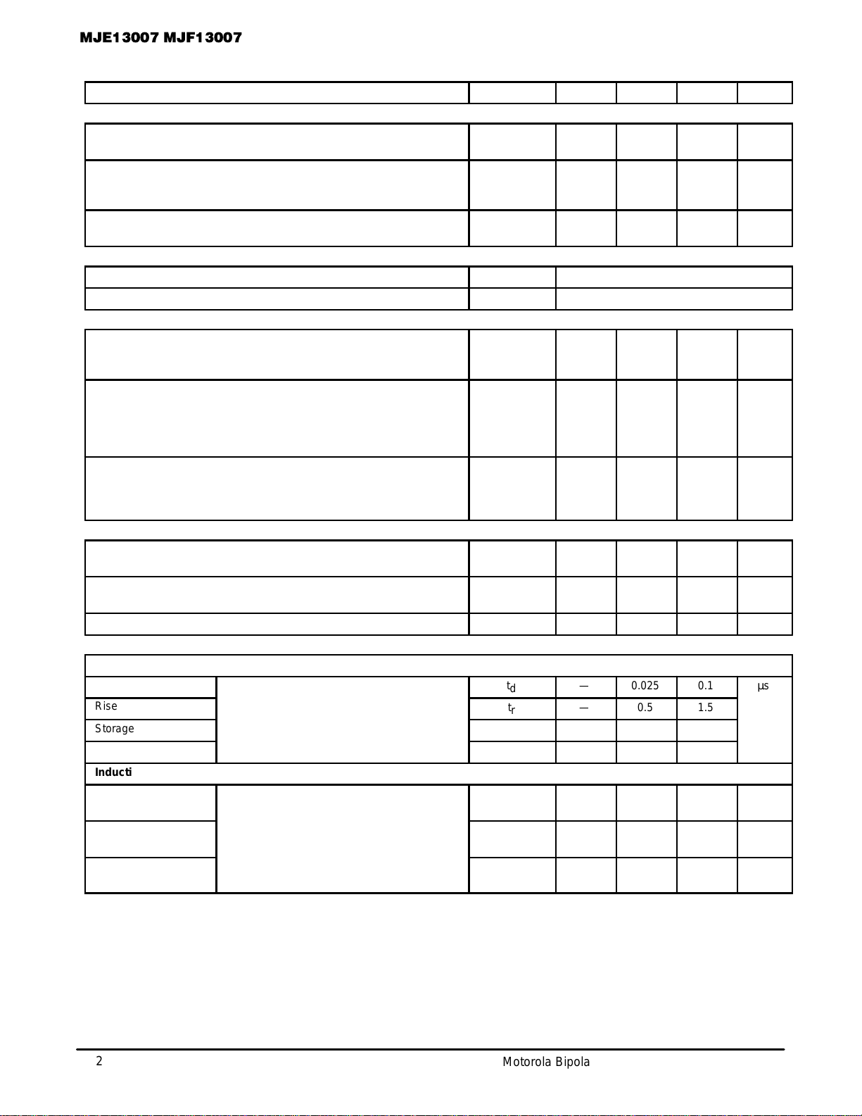
SWITCHING CHARACTERISTICS
Resistive Load (Table 1)
Delay Time
t
d
— 0.025 0.1 µs
Rise Time
t
r
— 0.5 1.5
Storage Time
IB1 = IB2 = 1.0 A, tp = 25 µs,
Duty Cycle ≤ 1.0%)
t
s
— 1.8 3.0
Fall Time
≤ 1.0%)
t
f
— 0.23 0.7
Inductive Load, Clamped (Table 1)
Voltage Storage Time VCC = 15 Vdc, IC = 5.0 A TC = 25°C
V
clamp
= 300 Vdc TC = 100°C
t
sv
—
—
1.2
1.6
2.0
3.0
µs
Crossover Time I
B(on)
= 1.0 A, I
B(off)
= 2.5 A TC = 25°C
LC = 200 µH TC = 100°C
t
c
—
—
0.15
0.21
0.30
0.50
µs
Fall Time TC = 25°C
TC = 100°C
t
fi
—
—
0.04
0.10
0.12
0.20
µs
* Pulse Test: Pulse Width ≤ 300 µs, Duty Cycle ≤ 2.0%.
(VCC = 125 Vdc, IC = 5.0 A,
3
Motorola Bipolar Power Transistor Device Data
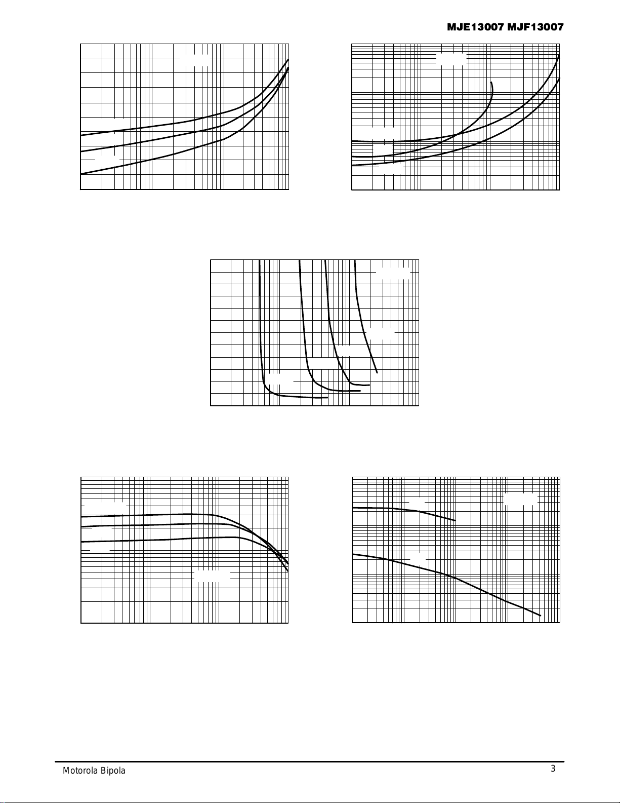
0.01 0.02 0.05 0.1 0.2 0.5 1 2 5 10
IC, COLLECTOR CURRENT (AMPS)
V
Figure 1. Base–Emitter Saturation Voltage
0.01
V
IC, COLLECTOR CURRENT (AMPS)
Figure 2. Collector–Emitter Saturation Voltage
0.01 0.02 0.05 0.1 0.2 0.5 1 2 3 5 10
IB, BASE CURRENT (AMPS)
Figure 3. Collector Saturation Region
V
CE
, COLLECTOR–EMITTER VOLTAGE (VOLTS)
0.01 0.1 1 10
h
FE
, DC CURRENT GAIN
IC, COLLECTOR CURRENT (AMPS)
Figure 4. DC Current Gain
0.1 1 10 100 1000
VR, REVERSE VOLTAGE (VOLTS)
Figure 5. Capacitance
C, CAPACITANCE (pF)
BE(sat)
, BASE–EMITTER SATURATION
VOLTAGE (VOLTS)
CE(sat)
, COLLECTOR–EMITTER SATURATION
VOLTAGE (VOLTS)
1.4
1.2
1
0.8
0.6
0.4
10
0.01
0.02
0.05
0.1
0.2
0.5
1
2
5
3
2.5
2
1.5
1
0.5
0
100
10
1
10000
1000
100
10
0.02 0.05 0.1 0.2 0.5 1 2 5 10
IC/IB = 5
TC = –40°C
25°C
100°C
IC/IB = 5
TC = –40°C
25°C
100°C
TJ = 25°C
IC = 8 A
IC = 5 A
IC = 3 A
IC = 1 A
TJ = 100°C
25°C
40°C
VCE = 5 V
C
ib
C
ob
TJ = 25°C
 Loading...