

1
Motorola Bipolar Power Transistor Device Data
For Isolated Package Applications
Designed for general–purpose amplifiers and switching applications, where the
mounting surface of the device is required to be electrically isolated from the heatsink
or chassis.
• Electrically Similar to the Popular TIP122 and TIP127
• 100 V
CEO(sus)
• 5 A Rated Collector Current
• No Isolating Washers Required
• Reduced System Cost
• High DC Current Gain — 2000 (Min) @ IC = 3 Adc
• UL Recognized, File #E69369, to 3500 V
RMS
Isolation
MAXIMUM RATINGS
Rating
Symbol
Value
ÎÎÎ
ÎÎÎ
ÎÎÎ
Unit
Collector–Emitter Voltage
V
CEO
100
ÎÎÎ
ÎÎÎ
ÎÎÎ
Vdc
Collector–Base Voltage
V
CB
100
ÎÎÎ
ÎÎÎ
ÎÎÎ
Vdc
Emitter–Base Voltage
V
EB
5
ÎÎÎ
ÎÎÎ
ÎÎÎ
Vdc
RMS Isolation Voltage (1) Test No. 1 Per Fig. 14
(for 1 sec, R.H. < 30%, Test No. 2 Per Fig. 15
TA = 25_C) Test No. 3 Per Fig. 16
V
ISOL
4500
3500
1500
ÎÎÎ
ÎÎÎ
ÎÎÎ
ÎÎÎ
ÎÎÎ
V
RMS
Collector Current — Continuous
Peak
I
C
5
8
ÎÎÎ
ÎÎÎ
ÎÎÎ
Adc
Base Current
I
B
0.12
ÎÎÎ
ÎÎÎ
ÎÎÎ
Adc
Total Power Dissipation* @ TC = 25_C
Derate above 25_C
P
D
30
0.24
ÎÎÎ
ÎÎÎ
ÎÎÎ
ÎÎÎ
Watts
W/_C
Total Power Dissipation @ TA = 25_C
Derate above 25_C
P
D
2
0.016
ÎÎÎ
ÎÎÎ
ÎÎÎ
ÎÎÎ
Watts
W/_C
Operating and Storage Junction Temperature Range
TJ, T
stg
–65 to +150
ÎÎÎ
ÎÎÎ
ÎÎÎ
I
C
THERMAL CHARACTERISTICS
Characteristic
Symbol
Max
ÎÎÎ
ÎÎÎ
ÎÎÎ
Unit
Thermal Resistance, Junction to Ambient
R
θJA
62.5
ÎÎÎ
ÎÎÎ
ÎÎÎ
_
C/W
Thermal Resistance, Junction to Case*
R
θJC
4.1
ÎÎÎ
ÎÎÎ
ÎÎÎ
_
C/W
Lead Temperature for Soldering Purpose
T
L
260
ÎÎÎ
ÎÎÎ
ÎÎÎ
_
C
*Measurement made with thermocouple contacting the bottom insulated mounting surface (in a location beneath the die), the device mounted on
a heatsink with thermal grease and a mounting torque of ≥ 6 in. lbs.
(1) Proper strike and creepage distance must be provided.
SEMICONDUCTOR TECHNICAL DATA
Order this document
by MF122/D
Motorola, Inc. 1995
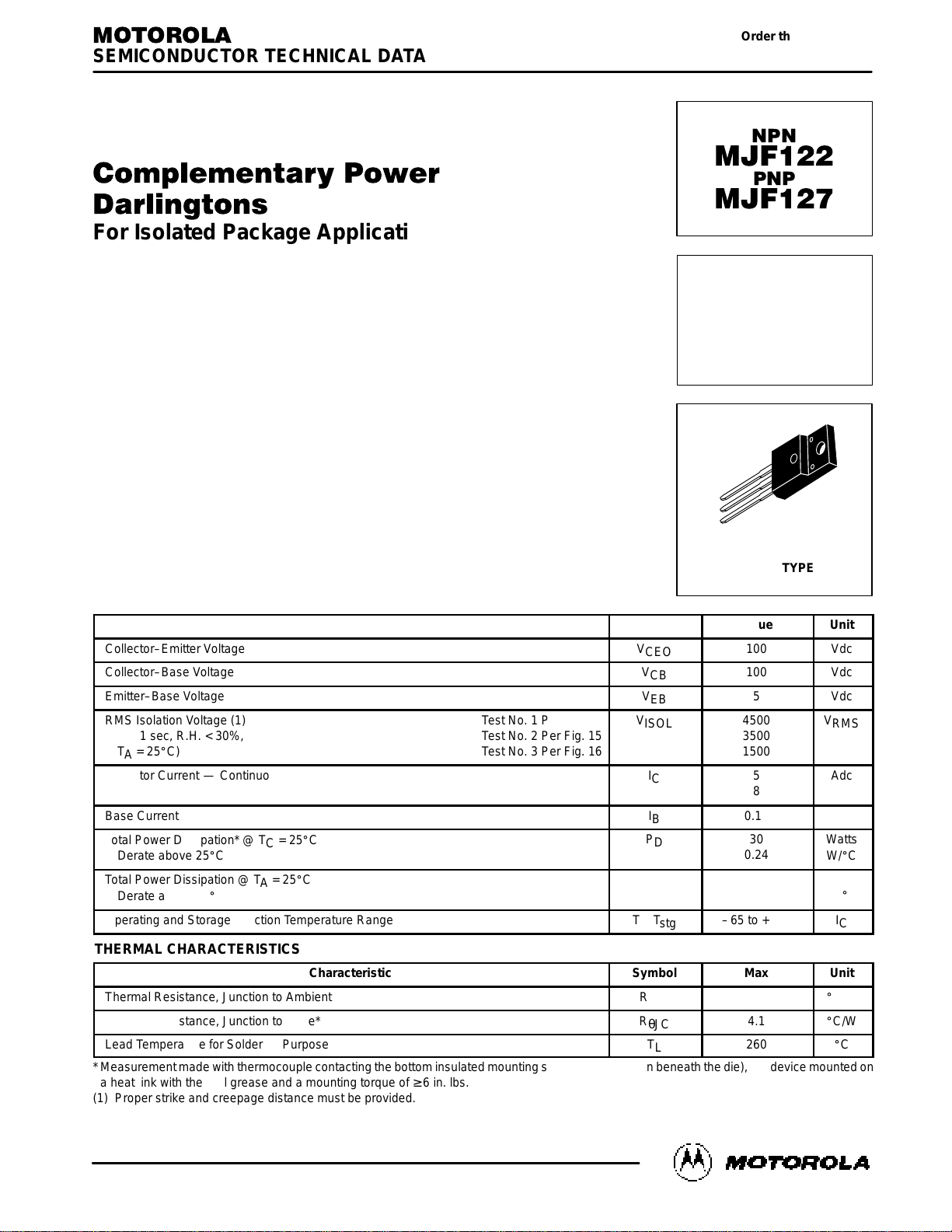
COMPLEMENTARY
SILICON
POWER DARLINGTONS
5 AMPERES
100 VOLTS
30 WATTS
CASE 221D–02
TO–220 TYPE
2
Motorola Bipolar Power Transistor Device Data
ELECTRICAL CHARACTERISTICS (T
C
= 25_C unless otherwise noted)
Characteristic
ÎÎÎÎ
ÎÎÎÎ
ÎÎÎÎ
Symbol
Min
Max
ÎÎÎ
ÎÎÎ
ÎÎÎ
Unit
OFF CHARACTERISTICS
Collector–Emitter Sustaining Voltage (1)
(IC = 100 mAdc, IB = 0)
ÎÎÎÎ
ÎÎÎÎ
ÎÎÎÎ
ÎÎÎÎ
V
CEO(sus)
100
—
ÎÎÎ
ÎÎÎ
ÎÎÎ
ÎÎÎ
Vdc
Collector Cutoff Current
(VCE = 50 Vdc, IB = 0)
ÎÎÎÎ
ÎÎÎÎ
ÎÎÎÎ
ÎÎÎÎ
I
CEO
—
10
ÎÎÎ
ÎÎÎ
ÎÎÎ
ÎÎÎ
µAdc
Collector Cutoff Current
(VCB = 100 Vdc, IE = 0)
ÎÎÎÎ
ÎÎÎÎ
ÎÎÎÎ
I
CBO
—
10
ÎÎÎ
ÎÎÎ
ÎÎÎ
µAdc
Emitter Cutoff Current (VBE = 5 Vdc, IC = 0)
ÎÎÎÎ
ÎÎÎÎ
ÎÎÎÎ
I
EBO
—
2
ÎÎÎ
ÎÎÎ
ÎÎÎ
mAdc
ON CHARACTERISTICS (1)
DC Current Gain (IC = 0.5 Adc, VCE = 3 Vdc)
DC Current Gain (IC = 3 Adc, VCE = 3 Vdc)
ÎÎÎÎ
ÎÎÎÎ
ÎÎÎÎ
ÎÎÎÎ
h
FE
1000
2000
—
—
ÎÎÎ
ÎÎÎ
ÎÎÎ
ÎÎÎ
—
Collector–Emitter Saturation Voltage (IC = 3 Adc, IB = 12 mAdc)
Collector–Emitter Saturation Voltage (IC = 5 Adc, IB = 20 mAdc)
ÎÎÎÎ
ÎÎÎÎ
ÎÎÎÎ
ÎÎÎÎ
V
CE(sat)
—
—
2
3.5
ÎÎÎ
ÎÎÎ
ÎÎÎ
ÎÎÎ
Vdc
Base–Emitter On Voltage (IC = 3 Adc, VCE = 3 Vdc)
ÎÎÎÎ
ÎÎÎÎ
ÎÎÎÎ
V
BE(on)
—
2.5
ÎÎÎ
ÎÎÎ
ÎÎÎ
Vdc
DYNAMIC CHARACTERISTICS
Small–Signal Current Gain (IC = 3 Adc, VCE = 4 Vdc, f = 1 MHz)
ÎÎÎÎ
ÎÎÎÎ
ÎÎÎÎ
h
fe
4
—
ÎÎÎ
ÎÎÎ
ÎÎÎ
—
Output Capacitance MJF127
(VCB = 10 Vdc, IE = 0, f = 0.1 MHz) MJF122
ÎÎÎÎ
ÎÎÎÎ
ÎÎÎÎ
ÎÎÎÎ
C
ob
—
—
300
200
ÎÎÎ
ÎÎÎ
ÎÎÎ
ÎÎÎ
pF
(1) Pulse Test: Pulse Width v 300 µs, Duty Cycle v 2%.
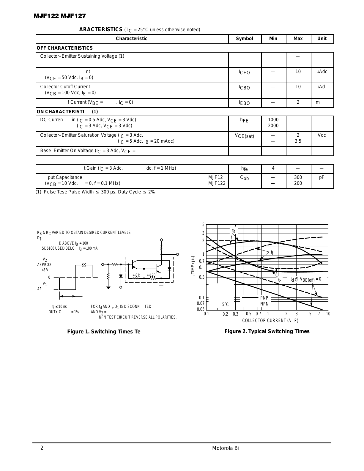
Figure 1. Switching Times Test Circuit
VCC = 30 V
IC/IB = 250
IB1 = I
B2
TJ = 25
°
C
0.1 0.7 100.5
0.3
2 5
5
IC, COLLECTOR CURRENT (AMP)
td @ V
BE(off)
= 0 V
t, TIME ( s)
µ
2
1
0.5
0.2
0.1
0.05
Figure 2. Typical Switching Times
t
s
t
f
0.3
3
0.2
1
0.07
0.7
3 7
PNP
NPN
≈
120
≈
8 k
V
2
APPROX.
+8 V
V
1
APPROX.
–12 V
25
µ
s
R
B
51
D
1
+4 V
V
CC
–30 V
R
C
SCOPE
TUT
tr, tf
≤
10 ns
DUTY CYCLE = 1%
FOR td AND tr, D1 IS DISCONNECTED
AND V2 = 0
FOR NPN TEST CIRCUIT REVERSE ALL POLARITIES.
RB & RC VARIED TO OBTAIN DESIRED CURRENT LEVELS
D1, MUST BE FAST RECOVERY TYPES, e.g.,
1N5825 USED ABOVE IB
≈
100 mA
MSD6100 USED BELOW IB
≈
100 mA
t
r
0

3
Motorola Bipolar Power Transistor Device Data
P
D
, POWER DISSIPATION (WATTS)
0
80
60
40
20
4
3
2
1
TAT
C
0
Figure 3. Maximum Power Derating
T, TEMPERATURE (°C)
40 60 100 120 16080 140
T
C
20
t, TIME (ms)
0.01
0.1 0.5 10 20 50 100 200 500 5K 10K1 52
1
0.2
0.1
0.05
r(t), TRANSIENT THERMAL
SINGLE PULSE
R
θ
JC(t)
= r(t) R
θ
JC
T
J(pk)
– TC = P
(pk)
R
θ
JC
(t)
RESISTANCE (NORMALIZED)
Figure 4. Thermal Response
0.5
0.3
0.03
0.02
0.2
1K 2K30 3003
0.3
3K
T
A
VCE, COLLECTOR–EMITTER VOLTAGE (VOLTS)
Figure 5. Maximum Forward Bias
Safe Operating Area
1
10
1
30
CURRENT LIMIT
SECONDARY BREAKDOWN
LIMIT
THERMAL LIMIT @
TC = 25
°
C (SINGLE PULSE)
I
C
, COLLECTOR CURRENT (AMPS)
0.1
2 3 50
3
0.3
10
0.2
dc
TJ = 150°C
1 ms
5 ms
100 µs
2
5
0.5
5 10020
There are two limitations on the power handling ability of a
transistor: average junction temperature and second breakdown. Safe operating area curves indicate IC – VCE limits of
the transistor that must be observed for reliable operation;
i.e., the transistor must not be subjected to greater dissipation than the curves indicate.
The data of Figure 5 is based on T
J(pk)
= 150_C; TC is
variable depending on conditions. Secondary breakdown
pulse limits are valid for duty cycles to 10% provided T
J(pk)
< 150_C. T
J(pk)
may be calculated from the data in Figure 4.
At high case temperatures, thermal limitations will reduce the
power that can be handled to values less than the limitations
imposed by secondary breakdown.
 Loading...