1
Motorola Bipolar Power Transistor Device Data
NPN Bipolar Power Transistor
The MJE8503A transistor is designed for high voltage, high speed, power switching
in inductive circuits where fall time is c ritical. They are suited f or line operated
switchmode applications such as:
• Switching Regulators
• Inverters
• Solenoid and Relay Drivers
• Motor Controls
• Deflection Circuits
Featuring
• 1500 Volt Collector-Base Breakdown Capability
• Fast Switching:
180 ns Typical Fall Times
450 ns Typical Crossover Times
1.2 µs Typical Storage Times
• Low Collector-Emitter Leakage Current — 100 µA Max @ 1500 V
CES
MAXIMUM RATINGS
(TC = 25°C unless otherwise noted)
Rating
Symbol Value Unit
Collector-Emitter Voltage V
CEO(sus)
700 Vdc
Collector-Emitter Voltage V
CES
1500 Vdc
Collector-Base Voltage V
CBO
1500 Vdc
Emitter-Base Voltage V
EBO
5.0 Vdc
Collector Current — Continuous
Collector Current — Peak (1)
I
C
5.0
10
Adc
Collector Current — Continuous
Collector Current — Peak
I
B
I
BM
4.0
4.0
Adc
Total Power Dissipation @ TC = 25°C
@ TC = 100°C
Derate above 25°C
P
D
80
21
0.8
Watts
W/°C
Operating and Storage Temperature Range TJ, T
stg
–65 to +125 °C
THERMAL CHARACTERISTICS
Characteristic Symbol Max Unit
Thermal Resistance, Junction to Case R
θJC
1.25 °C/W
Maximum Lead Temperature for Soldering Purposes
1/8″ from Case for 5 sec.
T
L
275 °C
(1) Pulse Test: Pulse Width = 5.0 ms, Duty Cycle < 10%.
SWITCHMODE is a trademark of Motorola Inc.
This document contains information on a new product. Specifications and information herein are subject to change without notice.
Preferred devices are Motorola recommended choices for future use and best overall value.
SEMICONDUCTOR TECHNICAL DATA
Order this document
by MJE8503A/D
Motorola, Inc. 1995
POWER TRANSISTORS
5.0 AMPERES
1500 VOLTS — BV
CES
80 WATTS
*Motorola Preferred Device
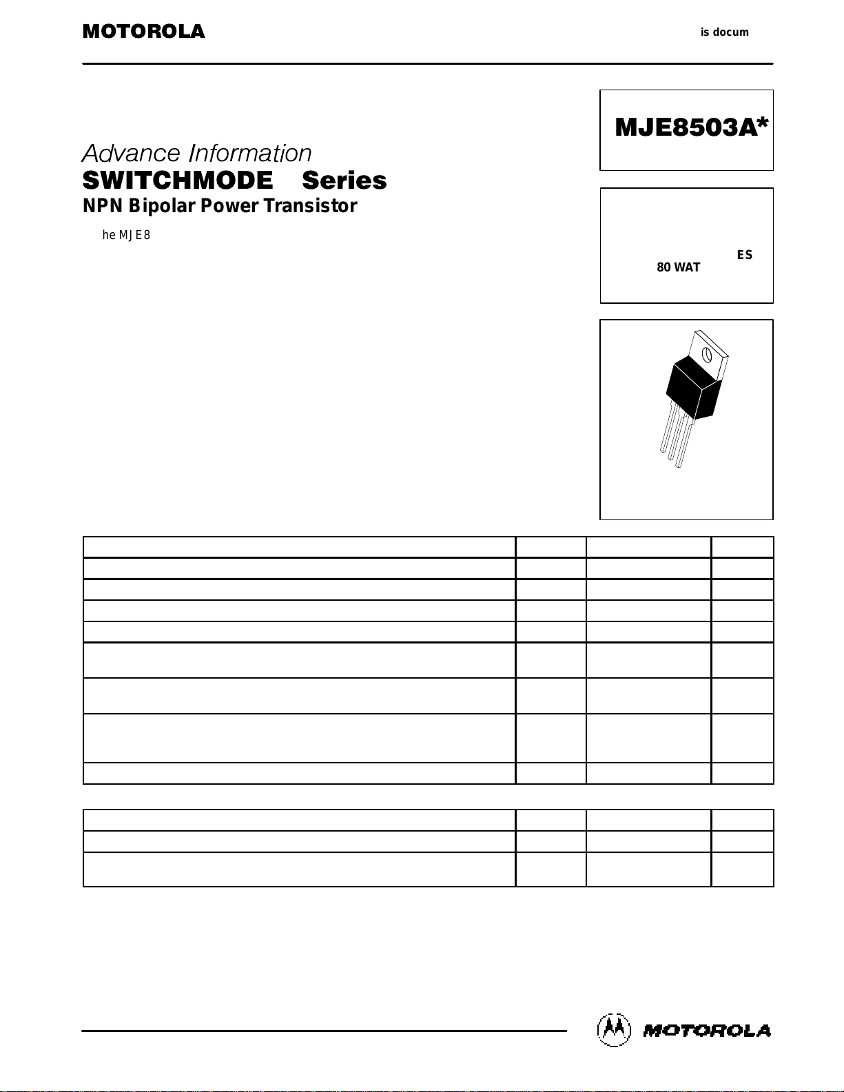
CASE 221A–06
TO–220AB

MJE8503A
2
Motorola Bipolar Power Transistor Device Data
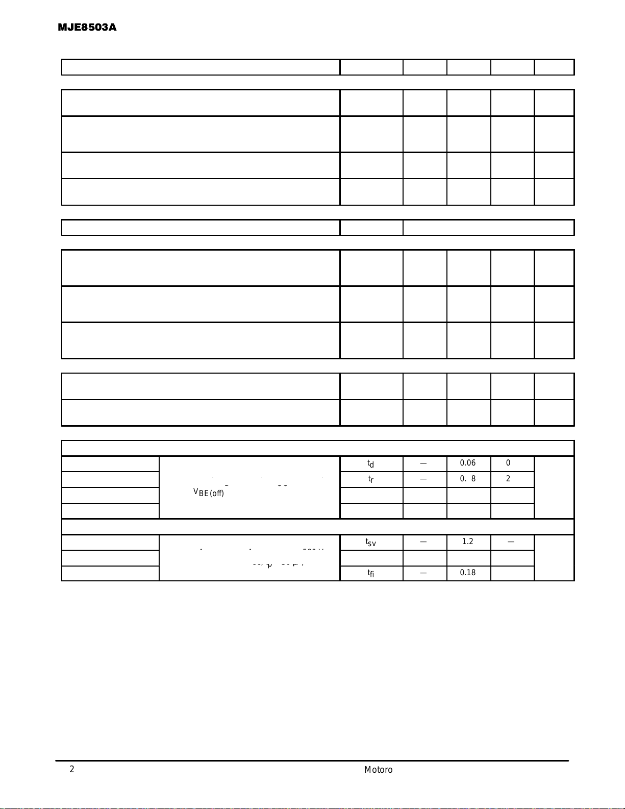
ELECTRICAL CHARACTERISTICS
(TC = 25°C unless otherwise noted)
Characteristic
Symbol Min Typ Max Unit
OFF CHARACTERISTICS
Collector-Emitter Sustaining Voltage
(IC = 100 mAdc, IB = 0)
V
CEO(sus)
700 — — Vdc
Collector Cutoff Current
(VCE = 1500 Vdc, VBE = 0, TC = 25°C)
(VCE = 1500 Vdc, VBE = 0, TC = 125°C)
I
CES
—
—
—
—
0.1
2.0
mAdc
Collector Cutoff Current
(VCE = 1500 Vdc, RBE = 50 Ohms, TC = 100°C)
I
CER
— — 5.0 mAdc
Emitter Cutoff Current
(VEB = 6.0 Vdc, IC = 0)
I
EBO
— — 1.0 mAdc
SECOND BREAKDOWN
Second Breakdown Collector with Base Forward Biased I
S/b
See Figure 2
ON CHARACTERISTICS
DC Current Gain
(IC = 1.0 Adc, VCE = 5.0 Vdc)
(IC = 4.5 Adc, VCE = 5.0 Vdc)
h
FE
7.5
2.25
—
—
—
—
—
Base-Emitter Saturation Voltage
(IC = 2.5 Adc, IB = 1.0 Vdc)
(IC = 4.5 Adc, IB = 2.0 Vdc)
V
BE(sat)
—
—
—
—
1.5
1.5
Vdc
Collector-Emitter Saturation Voltage
(IC = 2.5 Adc, IB = 1.0 Vdc)
(IC = 4.5 Adc, IB = 2.0 Vdc)
V
CE(sat)
—
—
—
—
2.0
3.0
Vdc
DYNAMIC CHARACTERISTICS
Current-Gain — Bandwidth Product
(IC = 0.1 Adc, VCE = 5.0 Vdc, f
test
= 1.0 MHz)
f
T
— 7.0 — MHz
Output Capacitance
(VCB = 10 Vdc, IE = 0, f
test
= 0.1 MHz)
C
ob
— 125 — pF
SWITCHING CHARACTERISTICS
Resistive Load (Table 1)
Delay Time
t
d
— 0.06 0.2
µs
Rise Time
C
= 2.5 Adc, IB = 1.0 Adc, VCC = 500 Vdc
t
r
— 0.08 2.0
Storage Time
(IC = 2.5 Adc, IB = 1.0 Adc, VCC = 500 Vdc
V
BE(off)
= 5.0 Vdc, tp = 50 µs)
t
s
— 1.2 4.0
Fall Time t
f
— 0.7 2.0
Inductive Load (Table 1)
Storage Time
t
sv
— 1.2 —
µs
Crossover Time
(IC = 2.5 Adc, IB = 1.0 Adc, V
clamp
= 500 Vdc
V
= 5.0 Vdc, t
= 50 µs)
t
c
— 0.45 —
Fall Time
V
BE(off)
= 5.0 Vdc, tp = 50 µs)
t
fi
— 0.18 —
(1) Pulse Test: Pulse Width = 300 µs, Duty Cycle ≤ 2%
(I
 Loading...