

MOTOROLA MGP7N60E Datasheet
SEMICONDUCTOR TECHNICAL DATA
N–Channel Enhancement–Mode Silicon Gate
Order this document
by MGP7N60E/D
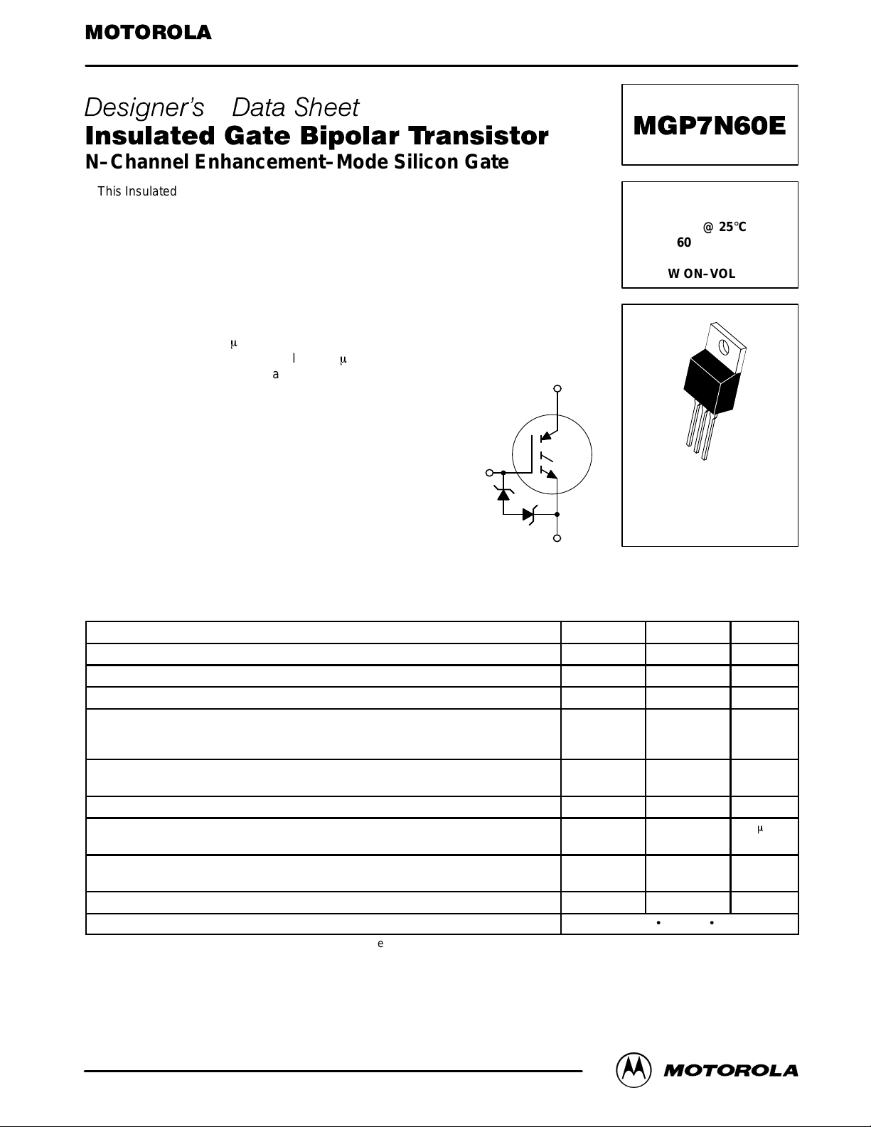
This Insulated Gate Bipolar Transistor (IGBT) uses an advanced
termination scheme to provide an enhanced and reliable high
voltage–blocking capability. Its new 600 V IGBT technology is
specifically suited for applications requiring both a high temperature short circuit capability and a low V
. It also provides fast
CE(on)
switching characteristics and results in efficient operation at high
frequencies. This new E–series introduces an energy efficient,
ESD protected, and short circuit rugged device.
• Industry Standard TO–220 Package
• High Speed: E
= 70 mJ/A typical at 125°C
off
• High Voltage Short Circuit Capability – 10 ms minimum at 125°C, 400 V
• Low On–Voltage 2.0 V typical at 5.0 A, 125°C
• Robust High Voltage Termination
• ESD Protection Gate–Emitter Zener Diodes
G
IGBT IN TO–220
7.0 A @ 90°C
10 A @ 25°C
600 VOL TS
SHORT CIRCUIT RATED
LOW ON–VOLTAGE
C
G
C
E
CASE 221A–09
STYLE 9
E
TO–220AB
MAXIMUM RATINGS
Collector–Emitter Voltage V
Collector–Gate Voltage (RGE = 1.0 MΩ) V
Gate–Emitter Voltage — Continuous V
Collector Current — Continuous @ TC = 25°C
Collector Current — Continuous @ TC = 90°C
Collector Current — Repetitive Pulsed Current (1)
Total Power Dissipation @ TC = 25°C
Derate above 25°C
Operating and Storage Junction Temperature Range TJ, T
Short Circuit Withstand Time
(VCC = 400 Vdc, VGE = 15 Vdc, TJ = 125°C, RG = 20 Ω)
Thermal Resistance — Junction to Case – IGBT
Thermal Resistance — Junction to Ambient
Maximum Lead Temperature for Soldering Purposes, 1/8″ from case for 5 seconds T
Mounting Torque, 6–32 or M3 screw
(1) Pulse width is limited by maximum junction temperature. Repetitive rating.
Designer’s Data for “Worst Case” Conditions — The Designer’s Data Sheet permits the design of most circuits entirely from the information presented. SOA Limit
curves — representing boundaries on device characteristics — are given to facilitate “worst case” design.
Designer’s is a trademark of Motorola, Inc.
(TJ = 25°C unless otherwise noted)
Rating Symbol Value Unit
CES
CGR
GE
I
C25
I
C90
I
CM
P
D
stg
t
sc
R
θJC
R
θJA
L
10 lbfSin (1.13 NSm)
600 Vdc
600 Vdc
±20 Vdc
10
7.0
14
81
0.65
–55 to 150 °C
10
1.5
65
260 °C
Adc
Apk
Watts
W/°C
m
°C/W
s
Motorola IGBT Device Data
Motorola, Inc. 1998
1
MGP7N60E
)
f = 1.0 MHz)
)
R
G
Ω)
)
R
G
T
J
125 C)
)
V
GE
Vdc)
ELECTRICAL CHARACTERISTICS
OFF CHARACTERISTICS
Collector–to–Emitter Breakdown Voltage
(VGE = 0 Vdc, IC = 25 µAdc)
T emperature Coef ficient (Positive)
Emitter–to–Collector Breakdown Voltage (VGE = 0 Vdc, IEC = 100 mAdc) V
Zero Gate Voltage Collector Current
(VCE = 600 Vdc, VGE = 0 Vdc)
(VCE = 600 Vdc, VGE = 0 Vdc, TJ = 125°C)
Gate–Body Leakage Current (VGE = ± 20 Vdc, VCE = 0 Vdc) I
ON CHARACTERISTICS (1)
Collector–to–Emitter On–State Voltage
(VGE = 15 Vdc, IC = 2.5 Adc)
(VGE = 15 Vdc, IC = 2.5 Adc, TJ = 125°C)
(VGE = 15 Vdc, IC = 5.0 Adc)
Gate Threshold Voltage
(VCE = VGE, IC = 1.0 mAdc)
Threshold Temperature Coefficient (Negative)
Forward Transconductance (VCE = 10 Vdc, IC = 5.0 Adc) g
DYNAMIC CHARACTERISTICS
Input Capacitance
Output Capacitance
Transfer Capacitance
SWITCHING CHARACTERISTICS (1)
Turn–On Delay Time
Rise Time
Turn–Off Delay Time
Fall Time
Turn–Off Switching Loss E
Turn–On Delay Time
Rise Time
Turn–Off Delay Time
Fall Time
Turn–Off Switching Loss E
Gate Charge
INTERNAL PACKAGE INDUCTANCE
Internal Emitter Inductance
(Measured from the emitter lead 0.25″ from package to emitter bond pad)
(1) Pulse Test: Pulse Width ≤ 300 µs, Duty Cycle ≤ 2%.
(T
= 25°C unless otherwise noted)
J
Characteristic
(VCE = 25 Vdc, VGE = 0 Vdc,
(VCC = 360 Vdc, IC = 5.0 Adc,
VGE = 15 Vdc, L = 300 mH,
Energy losses include “tail”
(VCC = 360 Vdc, IC = 5.0 Adc,
VGE = 15 Vdc, L = 300 mH,
Energy losses include “tail”
(VCC = 360 Vdc, IC = 5.0 Adc,
R
= 20 Ω, T
= 20 Ω,
f = 1.0 MHz
R
= 20 Ω
= 20
V
= 15 Vdc
= 15
= 125°C
=
Symbol Min Typ Max Unit
V
(BR)CES
(BR)ECS
I
CES
GES
V
CE(on)
V
GE(th)
fe
C
ies
C
oes
C
res
t
d(on)
t
r
t
d(off)
t
f
off
t
d(on)
t
r
t
d(off)
t
f
off
Q
T
Q
1
Q
2
L
E
600
—
15 — — Vdc
—
—
— — 50
—
—
—
4.0
—
— 2.5 — Mhos
— 610 —
— 60 —
— 10 —
— 22 —
— 24 —
— 64 —
— 196 —
— 0.20 0.34 mJ
— 31 —
— 24 —
— 195 —
— 220 —
— 0.35 — mJ
— 27.2 —
— 7.0 —
— 13.7 —
— 7.5 —
—
870
—
—
1.6
1.5
2.0
6.0
10
—
—
10
200
1.9
—
2.4
8.0
—
mV/°C
µAdc
m
mV/°C
Vdc
Adc
Vdc
Vdc
pF
ns
ns
nC
nH
2
Motorola IGBT Device Data
 Loading...