

MOTOROLA MGP4N60ED Datasheet
SEMICONDUCTOR TECHNICAL DATA
N–Channel Enhancement–Mode Silicon Gate
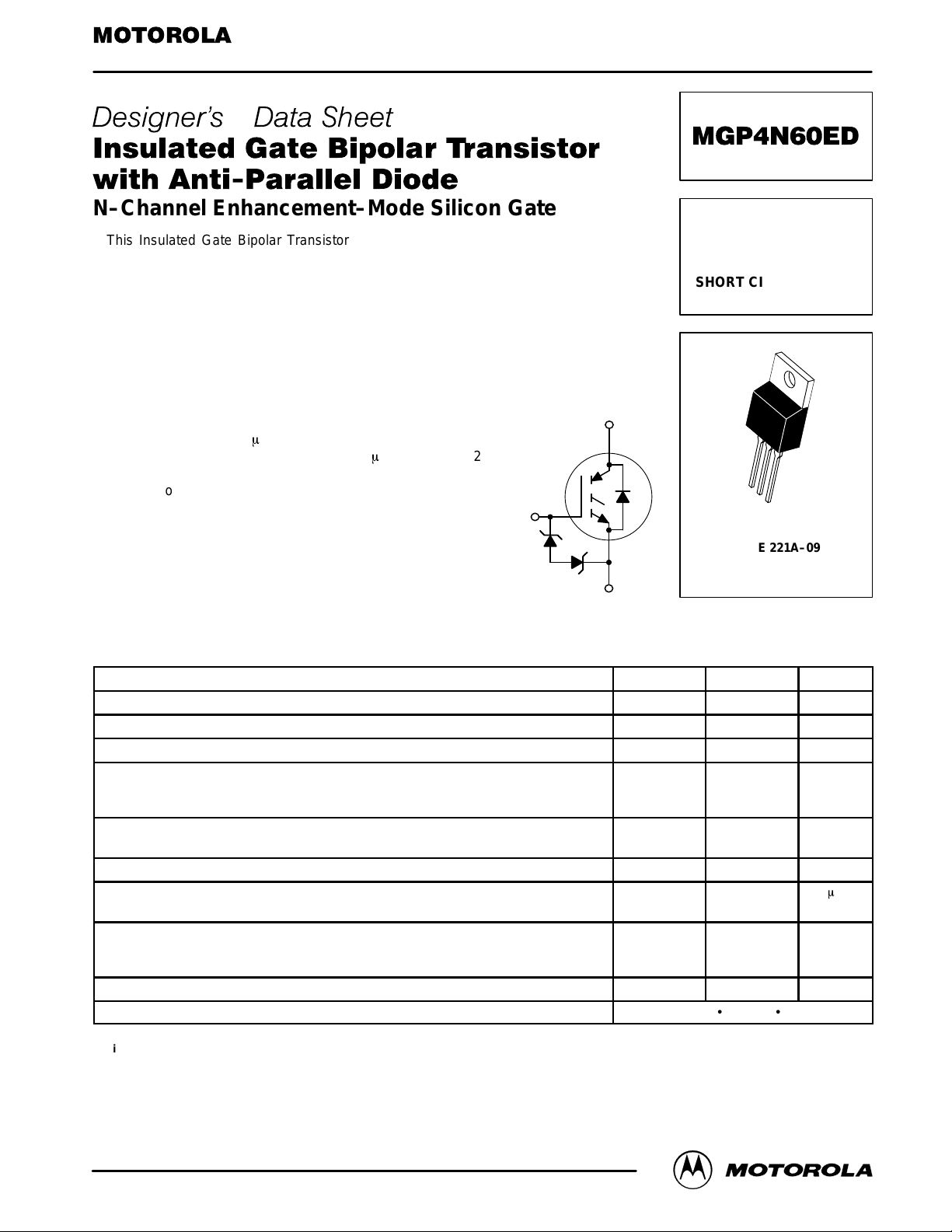
This Insulated Gate Bipolar Transistor (IGBT) is co–packaged
with a soft recovery ultra–fast rectifier and uses an advanced
termination scheme to provide an enhanced and reliable high
voltage–blocking capability. Its new 600 V IGBT technology is
specifically suited for applications requiring both a high temperature short circuit capability and a low V
switching characteristics and results in efficient operation at high
frequencies. Co–packaged IGBTs save space, reduce assembly
time and cost. This new E–series introduces an energy efficient,
ESD protected and short circuit rugged device.
. It also provides fast
CE(on)
Order this document
by MGP4N60ED/D
IGBT & DIODE IN TO–220
4.0 A @ 90°C
6.0 A @ 25°C
600 VOL TS
SHORT CIRCUIT RATED
LOW ON–VOLTAGE
• Industry Standard TO–220 Package
• High Speed: E
= 60 mJ/A typical at 125°C
off
C
• High Voltage Short Circuit Capability – 10 ms minimum at 125°C, 400 V
• Low On–Voltage 2.0 V typical at 3.0 A, 125°C
• Soft Recovery Free Wheeling Diode
is Included in the Package
• Robust High Voltage Termination
G
• ESD Protection Gate–Emitter Zener Diodes
E
MAXIMUM RATINGS
Collector–Emitter Voltage V
Collector–Gate Voltage (RGE = 1.0 MΩ) V
Gate–Emitter Voltage — Continuous V
Collector Current — Continuous @ TC = 25°C
Total Power Dissipation @ TC = 25°C
Derate above 25°C
Operating and Storage Junction Temperature Range TJ, T
Short Circuit Withstand Time
(VCC = 400 Vdc, VGE = 15 Vdc, TJ = 125°C, RG = 20 Ω)
Thermal Resistance — Junction to Case – IGBT
Maximum Lead Temperature for Soldering Purposes, 1/8″ from case for 5 seconds T
Mounting Torque, 6–32 or M3 screw
(1) Pulse width is limited by maximum junction temperature. Repetitive rating.
Designer’s Data for “Worst Case” Conditions — The Designer’s Data Sheet permits the design of most circuits entirely from the information presented. SOA Limit
curves — representing boundaries on device characteristics — are given to facilitate “worst case” design.
Designer’s is a trademark of Motorola, Inc.
(TJ = 25°C unless otherwise noted)
Rating Symbol Value Unit
— Continuous @ TC = 90°C
— Repetitive Pulsed Current (1)
— Junction to Case – Diode
— Junction to Ambient
CES
CGR
GE
I
C25
I
C90
I
CM
P
D
stg
t
sc
R
θJC
R
θJC
R
θJA
L
10 lbfSin (1.13 NSm)
G
C
E
CASE 221A–09
STYLE 9
TO–220AB
600 Vdc
600 Vdc
±20 Vdc
6.0
4.0
8.0
62.5
0.51
–55 to 150 °C
10
2.0
3.6
65
260 °C
Adc
Apk
Watts
W/°C
m
°C/W
s
REV 1
Motorola IGBT Device Data
Motorola, Inc. 1998
1
MGP4N60ED
)
f = 1.0 MHz)
)
R
G
Ω)
)
R
G
T
J
125 C)
)
V
GE
Vdc)
ELECTRICAL CHARACTERISTICS
OFF CHARACTERISTICS
Collector–to–Emitter Breakdown Voltage
(VGE = 0 Vdc, IC = 25 µAdc)
T emperature Coef ficient (Positive)
Zero Gate Voltage Collector Current
(VCE = 600 Vdc, VGE = 0 Vdc)
(VCE = 600 Vdc, VGE = 0 Vdc, TJ = 125°C)
Gate–Body Leakage Current (VGE = ± 20 Vdc, VCE = 0 Vdc) I
ON CHARACTERISTICS (1)
Collector–to–Emitter On–State Voltage
(VGE = 15 Vdc, IC = 1.5 Adc)
(VGE = 15 Vdc, IC = 1.5 Adc, TJ = 125°C)
(VGE = 15 Vdc, IC = 3.0 Adc)
Gate Threshold Voltage
(VCE = VGE, IC = 1.0 mAdc)
Threshold Temperature Coefficient (Negative)
Forward Transconductance (VCE = 10 Vdc, IC = 3.0 Adc) g
DYNAMIC CHARACTERISTICS
Input Capacitance
Output Capacitance
Transfer Capacitance
SWITCHING CHARACTERISTICS (1)
Turn–On Delay Time
Rise Time
Turn–Off Delay Time
Fall Time
Turn–Off Switching Loss
Turn–On Switching Loss E
Total Switching Loss E
Turn–On Delay Time
Rise Time
Turn–Off Delay Time
Fall Time
Turn–Off Switching Loss
Turn–On Switching Loss E
Total Switching Loss E
Gate Charge
(1) Pulse Test: Pulse Width ≤ 300 µs, Duty Cycle ≤ 2%.
(T
= 25°C unless otherwise noted)
J
Characteristic
(VCE = 25 Vdc, VGE = 0 Vdc,
(VCC = 360 Vdc, IC = 3.0 Adc,
VGE = 15 Vdc, L = 300 mH,
Energy losses include “tail”
(VCC = 360 Vdc, IC = 3.0 Adc,
VGE = 15 Vdc, L = 300 mH,
Energy losses include “tail”
(VCC = 360 Vdc, IC = 3.0 Adc,
R
= 20 Ω, T
= 20 Ω,
f = 1.0 MHz
R
= 20 Ω
= 20
V
= 15 Vdc
= 15
= 125°C
=
Symbol Min Typ Max Unit
V
(BR)CES
I
CES
GES
V
CE(on)
V
GE(th)
fe
C
ies
C
oes
C
res
t
d(on)
t
r
t
d(off)
t
f
E
off
on
ts
t
d(on)
t
r
t
d(off)
t
f
E
off
on
ts
Q
T
Q
1
Q
2
600
—
—
—
— — 50
—
—
—
4.0
—
— 1.8 — Mhos
— 342 —
— 40 —
— 3.0 —
— 34 —
— 30 —
— 36 —
— 216 —
— 100 150
— 25 —
— 125 —
— 33 —
— 32 —
— 56 —
— 340 —
— 170 —
— 50 —
— 220 —
— 18.1 —
— 3.8 —
— 7.8 —
—
870
—
—
1.6
1.5
2.0
6.0
10
—
—
10
200
1.9
—
2.4
8.0
—
mV/°C
µAdc
m
mV/°C
Vdc
Adc
Vdc
Vdc
pF
ns
m
ns
m
nC
J
J
2
Motorola IGBT Device Data
 Loading...