MOTOROLA MDC5101R2 Datasheet

1
Analog/Interface Integrated Circuit Device Data
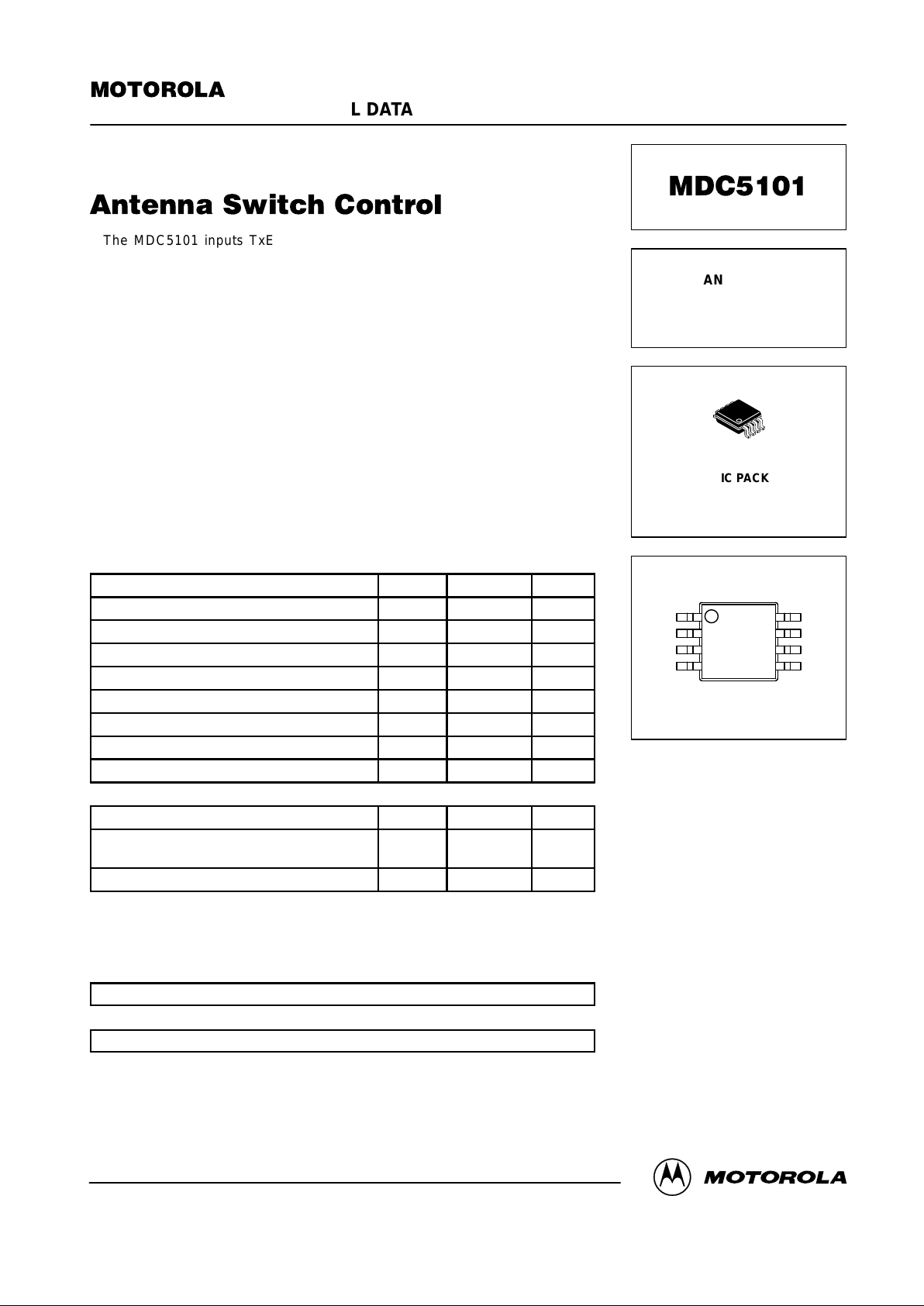
The MDC5101 inputs TxE and RxE Logic Signals with an accessory input
termination option and, allows positive and negative control voltages in accordance
with the enclosed truth table. This device is primarily intended to control GaAs RF
switches. It is also designed to interface with most HCMOS MCUs such as the
Motorola MC68338.
The MDC5101 is intended to replace a circuit of up to 18 discrete components and
is available in a Micro–8 package. This device, in combination with a compatible RF
switch, can be used to achieve duplex isolation in any Time Division Duplex Radio like
GSM and DCS1800 with staggered Transmit Receive Time Slots. It can also be used
to control an RF switch in dual band radio applications.
This integrated solution in a Micro–8 package compared with a discrete solution will
add a great value in performance with less board space consumption.
Features
• Miniature Micro–8 Surface Mount Package Saves Board Space
• Logic Level Control
• Designed to Interface with Microcontrollers
MAXIMUM RATINGS
Rating Symbol Value Unit
Positive Power Supply Voltage
(1)
V
CC
15 Vdc
Negative Power Supply Voltage
(2)
V
EE
–12 Vdc
Differential Power Supply Voltage VCC–V
EE
15 Vdc
Input Voltage
(3)
V
in
V
CC
Vdc
Output Current
(4)
I1, I
2
5.0 mAdc
Operating Temperature Range T
A
–40 to +85 °C
Storage Temperature Range T
stg
–55 to +150 °C
Junction Temperature T
J
150 °C
THERMAL CHARACTERISTICS
Characteristic Symbol Value Unit
Total Power Dissipation
Derate above 25°C
P
D
510
4.0
mW
mW/°C
Thermal Resistance, Junction to Ambient R
θJA
245 °C/W
Note 1: Pin 1 Referenced to Ground
Note 2: Pin 6 Referenced to Ground
Note 3: Pin 3, 4 Referenced to Ground
Note 4: Pin 5, 7 Referenced to Ground
DEVICE MARKING
5101
ORDERING INFORMATION
MDC5101R2 13 inch Reel, 4000 units
ESD Rating
ESD protection on each pin to ±2500 V per MIL–STD6883 method 3015, using human body model of 100 pF , 1500 Ohms and using the machine
model to ±200 V at 100 pF and 0 Ohms. Parts must meet electrical requirement after testing.
Order this document
by MDC5101/D
SEMICONDUCTOR TECHNICAL DATA
ANTENNA
SWITCH
CONTROLLER
PLASTIC PACKAGE
CASE 846A–02
(Micro–8)
GND
V1
V
EE
V2
V
CC
ACC
RXE
TXE
4
3
2
1
8
7
6
5
(Top View)
Motorola, Inc. 1999
REV 2

MDC5101
2
Analog/Interface Integrated Circuit Device Data
ELECTRICAL CHARACTERISTICS
(VCC = 2.75 V , VEE = –5.0 V , TA = T
low
to T
high
unless otherwise noted)
Characteristic Symbol Min Typ Max Unit
DC PARAMETERS
Positive Power Supply Current
V1, V2, ACC 10 kW to GND, RxE = VIH, TxE = V
IL
I
CC
— — 1.0
mA
Negative Power Supply Current
V1, V2, ACC Open, RxE = VIL, TxE = V
IH
I
EE
— –50 —
m
A
Negative Power Supply Current
V1, V2, ACC 10 kW to GND, RxE = VIL, TxE = V
IH
I
EE
–1.5 — —
mA
High Level Output Voltage
I1 = I2 = 250 mA, ACC Open
RxE = VIL, TxE = V
IH
RxE = VIH, TxE = V
IL
V
OH(V1)
V
OH(V2)
VIH–0.25
VIH–0.25
Vdc
I1 = I2 = 250 mA, ACC 10 kW to GND
RxE = VIL, TxE = V
IH
RxE = VIH, TxE = V
IL
V
OH(V2)
V
OH(V1)
VIH–0.25
VIH–0.25
Low Level Output Voltage
I1 = I2 = 250 mA, ACC Open
RxE = TxE = V
IL
RxE = VIH, TxE = V
IL
V
OL(V1,V2)
V
OL(V1)
–0.5
–0.5
0
0
0.5
0.5
Vdc
I1 = I2 = 250 mA, ACC 10 kW to GND
RxE = TxE = V
IL
RxE = VIH, TxE = V
IL
V
OL(V1,V2)
V
OL(V2)
–0.5
–0.5
0
0
0.5
0.5
Low Level Output Voltage
I1 = I2 = 250 mA, TxE = VIH, RxE = V
IL
ACC Open
ACC 10 kW to GND
V
OL(V2)
V
OL(V1)
–4.5
–4.5
Vdc
AC PARAMETERS
Propagation Delay
RxE, TxE to V1, V2
ACC Open
t
PLH
t
PHL
—
—
—
—
1.5
1.5
m
s
RxE, TxE to V1, V2
ACC 10 kW to GND
t
PLH
t
PHL
—
—
—
—
1.5
1.5
ACC to V1, V2 t
PLH
t
PHL
—
—
—
—
5.0
5.0
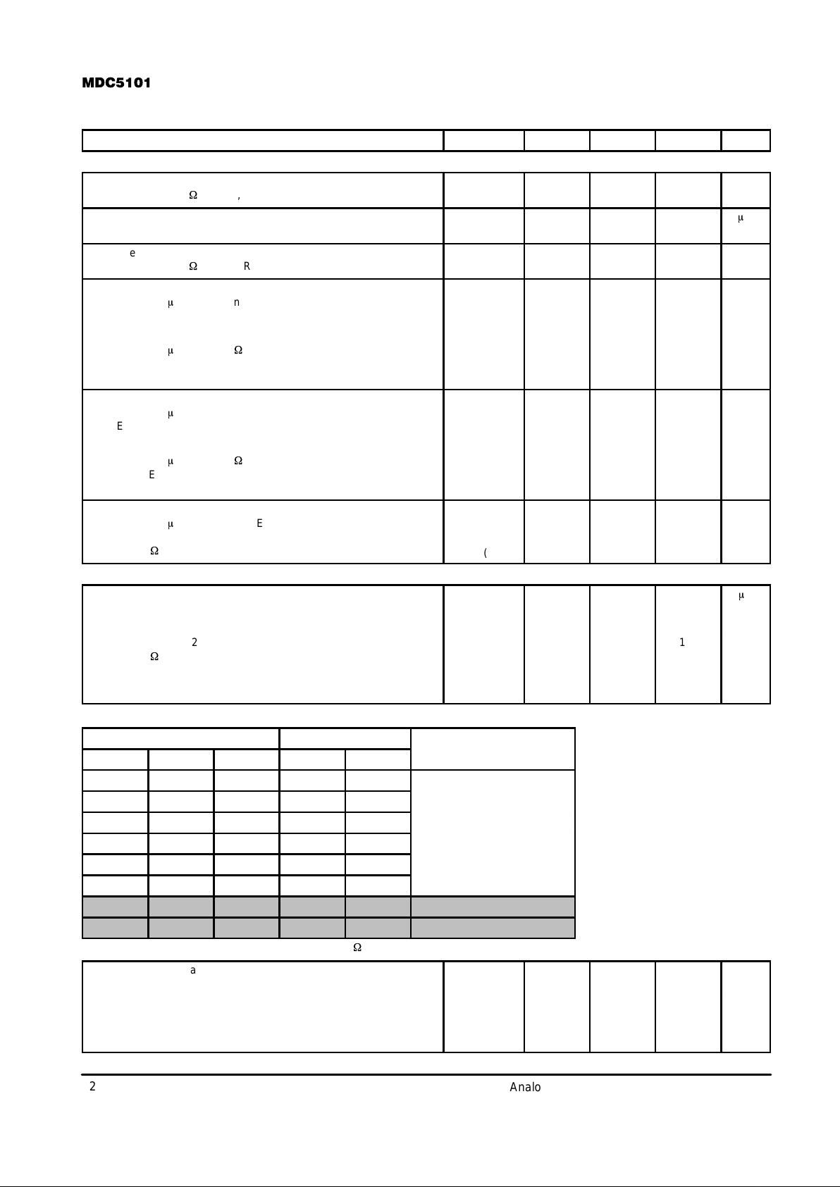
TRUTH TABLE
Input Logic Output Logic
RxE TxE ACC V2 V1
0 0 0 0 0
0 0 1 0 0
0 1 0 –5.0 2.7
0 1 1 2.7 –5.0
1 0 0 2.7 0
1 0 1 0 2.7
1 1 0 2.7 2.7 State not allowed in software
1 1 1 2.7 2.7 State not allowed in software
Note: ACC Logic Low = Open, ACC Logic High = 10 k
W
Low Level Input Voltage
RxE, TxE
V
IL
— — 0.4
Vdc
High Level Input Voltage
RxE, TxE
V
IH
2.5 — —
Maximum Voltage Differential VCC–V
IH
— — 1.5

MDC5101
3
Analog/Interface Integrated Circuit Device Data
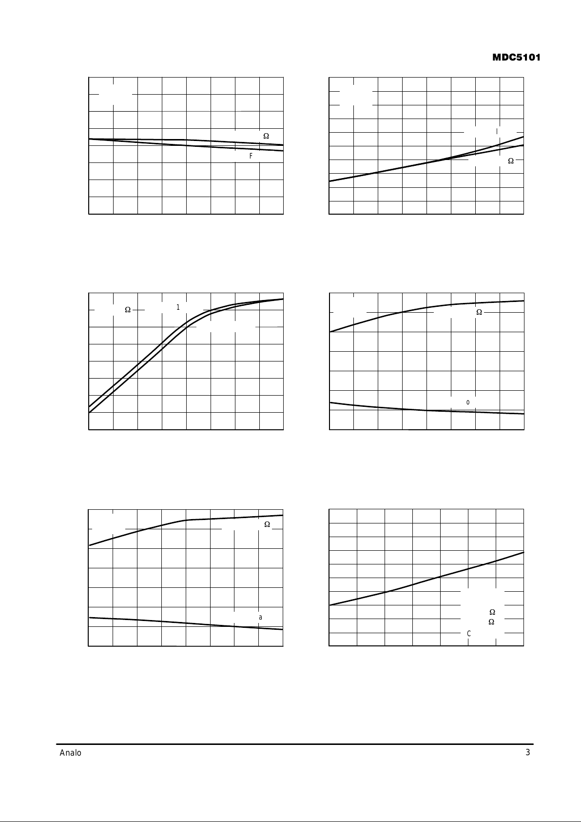
Figure 1. V
out (high)
versus Temperature Figure 2. V
out (low)
versus Temperature
Figure 3. ICC versus Temperature Figure 4. IEE versus Temperature
Figure 5. IEE versus Temperature Figure 6. IEE versus V
EE
85–40
TEMPERATURE (
°
C)
2.75
2.80
2.70
TEMPERATURE (
°
C)
–40
1.2
0.9
0.7
0.6
0.8
0.5
VEE (V)
–6–5
–1.9
–0.7
–0.5
–8
V
out
(V)
I
EE
(mA)
2.65
2.60
25
25 85
–7 –9 –10
I
EE
(mA)
V2 ACC 10 k
W
V1 ACC Floating
RX–E = 0
TX–E = 1
85–40
TEMPERATURE (
°
C)
–4.75
–4.65
–4.80
V
out
(V)
–4.85
–4.90
25
V1 ACC 10 k
W
V2 ACC Floating
RX–E = 0
TX–E = 1
–4.70
85–40
TEMPERATURE (
°
C)
0.60
0.65
0.55
I
CC
(mA)
0.50
0.45
25
ICC RX = 0, TX = 1
ACC 10 k
W
ICC RX = 1, TX = 0
1.1
1.0
RX–E = 0
TX–E = 1
IEE ACC 10 k
W
IEE ACC Floating
TEMPERATURE (
°
C)
–40
0.7
0.4
0.2
0.1
0.3
0
I
EE
(mA)
25 85
0.6
0.5
RX–E = 1
TX–E = 0
IEE ACC 10 k
W
IEE ACC Floating
–11 –12
–1.1
–0.9
–1.3
–1.7
–1.5
–2.5
–2.3
–2.1
RX–E = 0,
TX–E = 1,
ACC 10 k
W
,
V
out
10 k
W
,
VCC = 2.75 V
 Loading...