Motorola MDC5000T1 Datasheet

1
Motorola Small–Signal Transistors, FETs and Diodes Device Data
• Maintains Stable Bias Current in Various Discrete Bipolar Junction and Field
Effect Transistors
• Provides Stable Bias Using a Single Component Without Use of Emitter Ballast
and Bypass Components
• Operates Over a Wide Range of Supply Voltages Down to 1.8 Vdc
• Reduces Bias Current Variation Due to Temperature and Unit–to–Unit Parametric
Changes
• Consumes t 0.5 mW at VCC = 2.75 V
This device provides a reference voltage and acts as a DC feedback element
around an external discrete, NPN BJT or N–Channel FET. It allows the external
transistor to have its emitter/source directly grounded and still operate with a stable
collector/drain DC current. It is primarily intended to stabilize the bias of discrete RF
stages operating from a low voltage regulated supply, but can also be used to stabilize
the bias current of any linear stage in order to eliminate emitter/source bypassing and
achieve tighter bias regulation over temperature and unit variations. This device is
intended to replace a circuit of three to six discrete components and is available in a
SOT–143 package.
The combination of low supply voltage, low quiescent current drain, and small
package make it ideal for portable communications applications such as:
• Cellular Telephones
• Pagers
• PCN/PCS Portables
• PCMCIA RF Modems
• Cordless Phones
• Broadband Transceivers and Other Portable Wireless Products
MAXIMUM RATINGS
Rating Symbol Value Unit
Power Supply Voltage V
CC
15 Vdc
Ambient Operating Temperature Range T
A
–40 to +85 °C
Storage Temperature Range T
stg
–65 to +150 °C
Junction Temperature T
J
150 °C
Collector Emitter Voltage (Q2) V
CEO
–15 V
THERMAL CHARACTERISTICS
Characteristic Symbol Max Unit
Total Device Power Dissipation
(FR–5 PCB of 1″ × 0.75″ × 0.062″, TA = 25°C)
Derate above 25°C
P
D
225
1.8
mW
mW/°C
Thermal Resistance, Junction to Ambient R
θJA
556 °C/W
DEVICE MARKING
MDC5000T1 = E5
SMALLBLOCK is a trademark of Motorola, Inc.
Order this document
by MDC5000T1/D
SEMICONDUCTOR TECHNICAL DATA
SILICON
SMALLBLOCK
INTEGRATED CIRCUIT
CASE 318A–05, Style 9
SOT–143
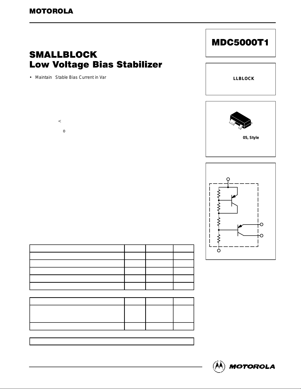
INTERNAL CIRCUIT DIAGRAM
VCC (3)
GND (1)
V
ref
(4)
I
out
(2)
Q1
Q2
R1
R2
R3
R4
Motorola, Inc. 1996

MDC5000T1
2
Motorola Small–Signal Transistors, FETs and Diodes Device Data
ELECTRICAL CHARACTERISTICS
(TA = 25°C unless otherwise noted)
Characteristic
Symbol Min Typ Max Unit
Recommended Operating Supply Voltage V
CC
1.8 2.75 10 Volts
Power Supply Current (VCC = 2.75 V)
V
ref
, I
out
are unterminated
See Figure 8
I
CC
— 110 200 µA
Q2 Collector Emitter Breakdown Voltage
(IC2 = 10 µA, IB2 = 0)
V
(BR)CEO2
–15 Volts
Reference Voltage (VCC = 2.75 V, V
out
= 0.7 V)
(I
out
= 30 µA)
(I
out
= 150 µA)
See Figure 9
V
ref
2.010
2.075
2.035
2.100
2.060
2.125
Volts
Reference Voltage (VCC = 2.75 V, V
out
= 0.7 V, –40°C ≤ TA ≤ +85°C)
VCC Pulse Width = 10 mS, Duty Cycle = 1.0%
(I
out
= 10 µA)
(I
out
= 30 µA)
(I
out
= 100 µA)
See Figure 9
D
V
ref
±5
±12
±25
±10
±25
±50
mV

MDC5000T1
3
Motorola Small–Signal Transistors, FETs and Diodes Device Data
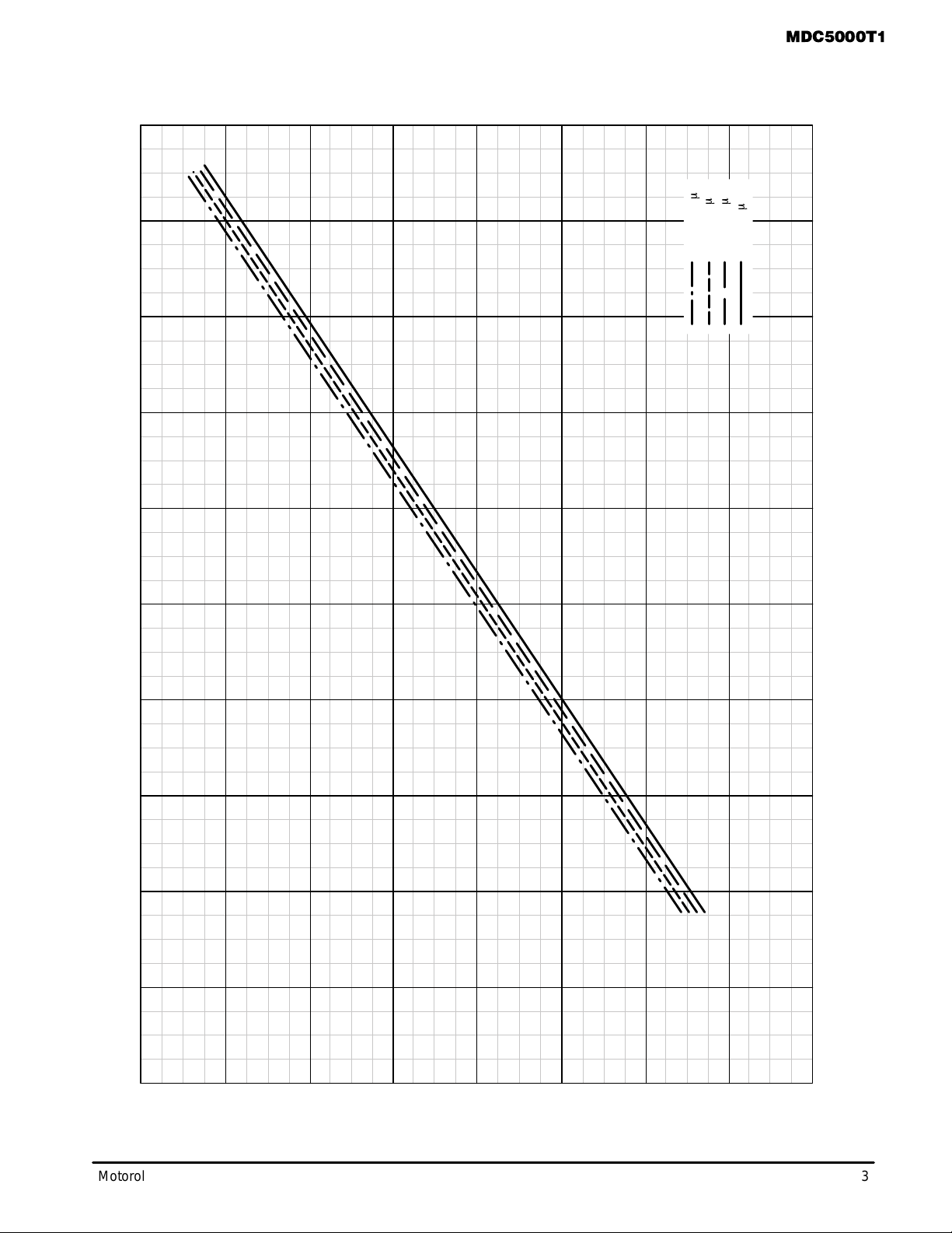
TYPICAL OPEN LOOP CHARACTERISTICS
(Refer to Circuit of Figure 9)
V
ref
(Vdc)
Figure 1. V
ref
versus VCC @ I
out
V , SUPPLY VOLTAGE (Vdc)
CC
109876543210
0
1
2
3
4
5
6
7
8
I
out
= 1000 A
m
I
out
= 500 A
m
I
out
= 100 A
m
I
out
= 10 A
m
 Loading...