

MOTOROLA MCR218 Technical data
MOTOROLA
查询MCR218/D供应商
SEMICONDUCTOR TECHNICAL DATA
Order this document
by MCR218/D
Thyristors
Silicon-Controlled Rectifiers
. . . designed primarily for half-wave ac control applications, such as motor controls,
heating controls and power supplies; or wherever half-wave silicon gate-controlled,
solid-state devices are needed.
• Glass-Passivated Junctions
• Blocking Voltage to 800 Volts
• TO-220 Construction — Low Thermal Resistance, High Heat Dissipation and
Durability
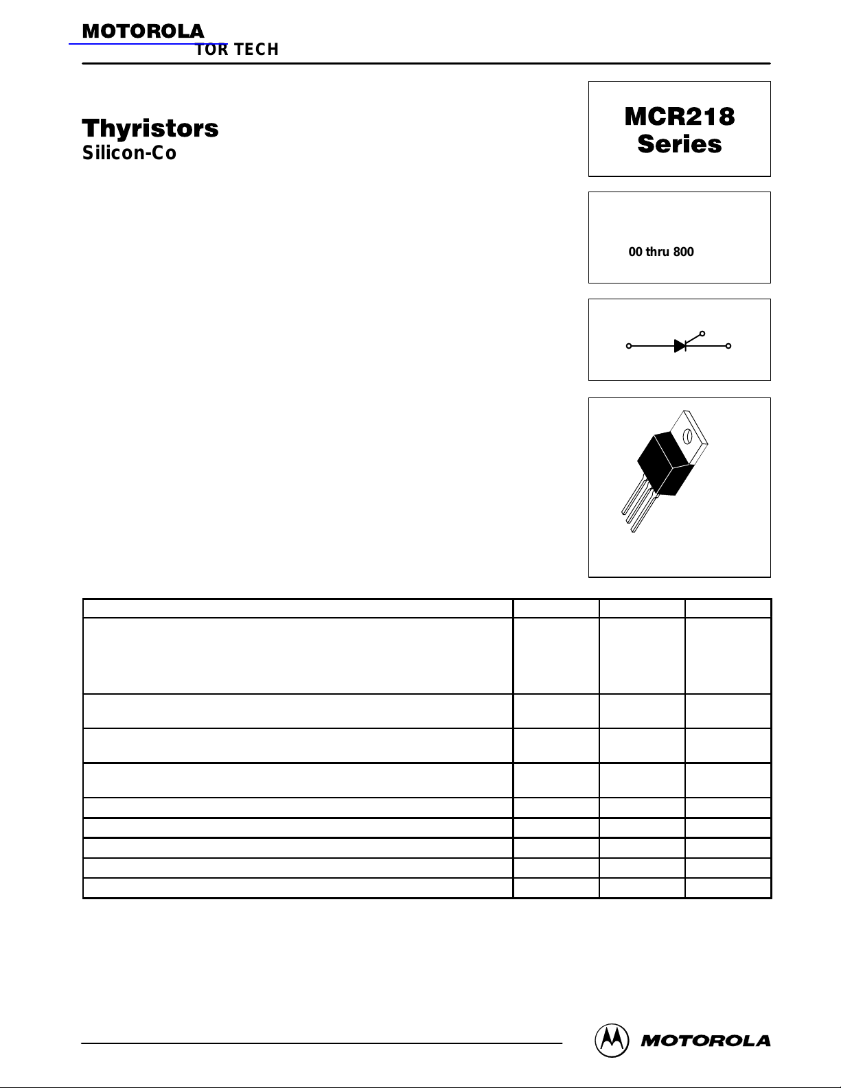
MCR218
Series
SCRs
8 AMPERES RMS
200 thru 800 VOL TS
G
A
K
CASE 221A-09
(TO-220AB)
STYLE 3
MAXIMUM RATINGS
Peak Repetitive Forward and Reverse Voltage
(TJ = 25 to 125°C, Gate Open) MCR218–4
Forward Current RMS
(All Conduction Angles)
Peak Forward Surge Current
(1/2 Cycle, Sine Wave, 60 Hz)
Circuit Fusing Considerations
(t = 8.3 ms)
Forward Peak Gate Power P
Forward Average Gate Power P
Forward Peak Gate Current I
Operating Junction Temperature Range T
Storage Temperature Range T
1. V
and V
DRM
voltage shall not be applied concurrent with negative potential on the anode. Blocking voltages shall not be tested with a constant current
source such that the voltage ratings of the devices are exceeded.
RRM
(TJ = 25°C unless otherwise noted.)
Rating Symbol Value Unit
(1)
MCR218–6
MCR218–8
MCR218–10
for all types can be applied on a continuous basis. Ratings apply for zero or negative gate voltage; however, positive gate
V
DRM
V
RRM
I
T(RMS)
I
TSM
I2t 26 A2s
GM
G(AV)
GM
J
stg
200
400
600
800
8 Amps
80 Amps
5 Watts
0.5 Watt
2 Amps
–40 to +125 °C
–40 to +150 °C
Volts
REV 1
Motorola Thyristor Device Data
Motorola, Inc. 1999
1
THERMAL CHARACTERISTICS
Characteristic Symbol Max Unit
Thermal Resistance, Junction to Case R
ELECTRICAL CHARACTERISTICS (T
Characteristic
Peak Forward or Reverse Blocking Current
(VAK = Rated V
Peak On-State Voltage
(ITM = 16 A Peak)
Gate Trigger Current (Continuous dc)
(VD = 12 V, RL = 100 Ohms)
Gate Trigger Voltage (Continuous dc)
(VD = 12 V, RL = 100 Ohms)
(Rated V
Holding Current
(Anode Voltage = 24 Vdc, Peak Initiating On-State Current = 0.5 A,
0.1 to 10 ms Pulse, Gate Trigger Source = 7 V, 20 Ohms)
Critical Rate-of-Rise of Off-State Voltage
(VD = Rated V
1. Pulse Test: Pulse Width = 1 ms, Duty Cycle p2%.
DRM
or V
DRM
(1)
, RL = 1000 Ohms, TJ = 125°C)
, Exponential Waveform, Gate Open, TJ = 125°C)
DRM
, Gate Open) TJ = 25°C
RRM
= 25°C unless otherwise noted.)
J
TJ = 125°C
Symbol Min Typ Max Unit
I
, I
DRM
RRM
V
TM
I
GT
V
GT
I
H
dv/dt — 100 — V/µs
θJC
—
—
— 1.5 1.8 Volts
— 10 25 mA
—
0.2
— 16 30 mA
2 °C/W
—
—
—
—
10
1.5
—
2
µA
mA
Volts
°
125
115
105
95
85
75
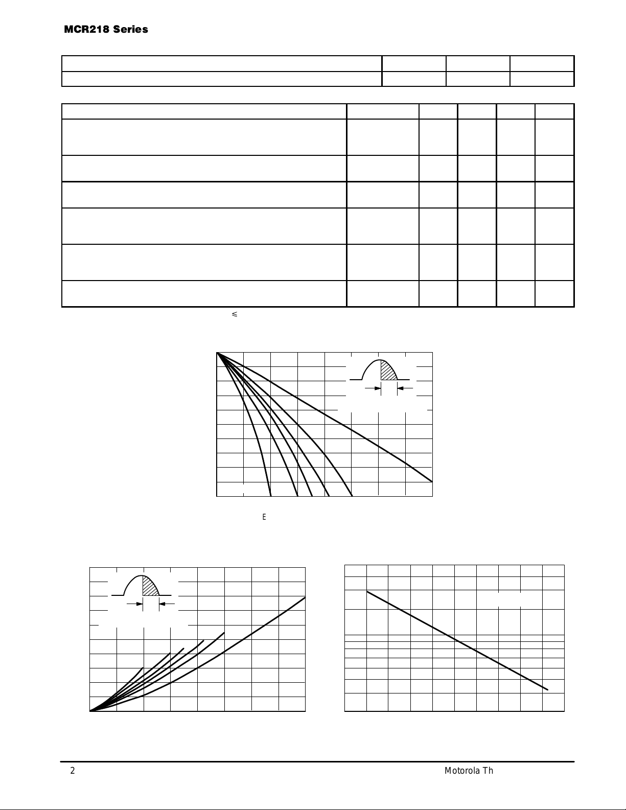
, MAXIMUM ALLOWABLE CASE TEMPERATURE ( C)
0
C
T
I
T(AV)
FIGURE 2 — ON-STATE POWER DISSIPATION
15
12
9.0
6.0
(WATTS)
α
= Conduction Angle
α
= 30
α
180
120
90
°
60
°
°
°
°
FIGURE 1 – CURRENT DERATING
α
α
= CONDUCTION ANGLE
α
= 30
°
, AVERAGE ON-STATE FORWARD CURRENT (AMPS)
60
°
90°120°180
°
FIGURE 3 — NORMALIZED GATE TRIGGER CURRENT
3.0
2.0
dc
1.5
1.0
0.9
0.7
dc
87654321
VD = 12 Vdc
3.0
, AVERAGE ON-STATE POWER DISSIP ATION
(AV)
P
0
0
I
, AVG. ON-STATE CURRENT (AMPS)
T(AV)
0.5
0.4
, NORMALIZED GATE TRIGGER CURRENT (mA)
0.3
GT
8.07.06.05.04.03.02.01.0
–60 120–40 0–20 20 40 60 80 100 140
I
TJ, JUNCTION TEMPERATURE (
°
C)
2 Motorola Thyristor Device Data
 Loading...