

Motorola MCM69L819AZP9R, MCM69L737AZP9, MCM69L737AZP9.5, MCM69L737AZP9.5R, MCM69L737AZP9R Datasheet
...
MOTOROLA
SEMICONDUCTOR TECHNICAL DATA
Advance Information
4M Late Write LVTTL
The MCM69L737A/819A is a 4 megabit synchronous late write fast static RAM
designed to provide high performance in secondary cache and ATM switch,
Telecom, and other high speed memory applications. The MCM69L819A
organized as 256K words by 18 bits, and the MCM69L737A organized as 128K
words by 36 bits wide are fabricated in Motorola’s high performance silicon gate
BiCMOS technology .
The differential CK clock inputs control the timing of read/write operations of
the RAM. At the rising edge of the CK clock all addresses, write enables, and
synchronous selects are registered. An internal buffer and special logic enable
the memory to accept write data on the rising edge of the CK clock a cycle after
address and control signals. Read data is available at the falling edge of the CK
clock.
The RAM uses L VTTL 3.3 V inputs and outputs.
The synchronous write and byte enables allow writing to individual bytes or the
entire word.
• Byte Write Control
• Single 3.3 V + 10%, – 5% Operation
• LVTTL 3.3 V I/O (V
• Register to Latch Synchronous Operation
• Asynchronous Output Enable
• Boundary Scan (JTAG) IEEE 1149.1 Compatible
• Differential Clock Inputs
• Optional x18 or x36 organization
• MCM69L737A/819A–8.5 = 8.5 ns
MCM69L737A/819A–9 = 9 ns
MCM69L737A/819A–9.5 = 9.5 ns
• Sleep Mode Operation (ZZ Pin)
• 1 19 Bump, 50 mil (1.27 mm) Pitch, 14 mm x 22 mm Plastic Ball Grid Array
(PBGA) Package
DDQ
)
Order this document
by MCM69L737A/D
MCM69L737A
MCM69L819A
ZP PACKAGE
PBGA
CASE 999–01
This document contains information on a new product. Specifications and information herein are subject to change without notice.
REV 1
8/15/97
Motorola, Inc. 1997
MOTOROLA FAST SRAM
MCM69L737A•MCM69L819A
1
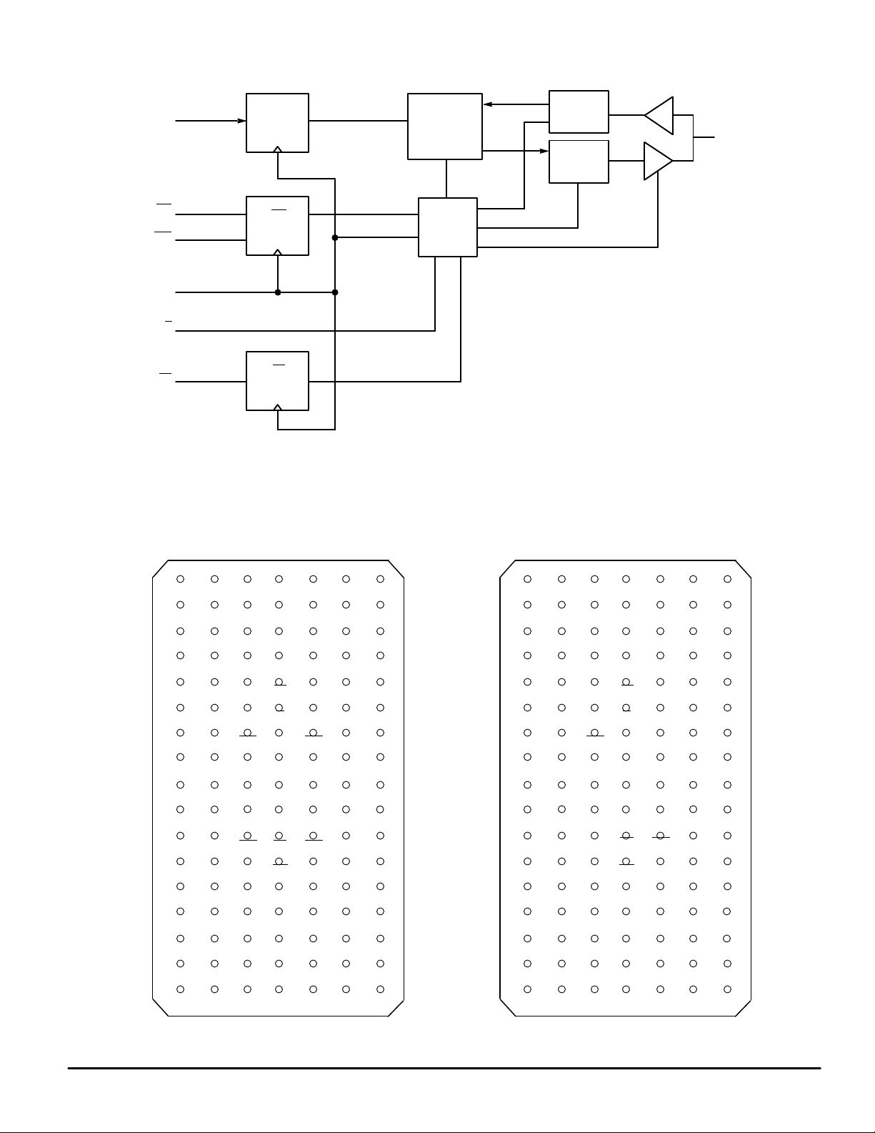
FUNCTIONAL BLOCK DIAGRAM
SA
SW
SBx
CK
SS
ADDRESS
REGISTERS
SW
REGISTERS
G
SS
REGISTERS
MEMORY
ARRAY
CONTROL
LOGIC
DATA IN
REGISTER
DQ
DATA OUT
LATCH
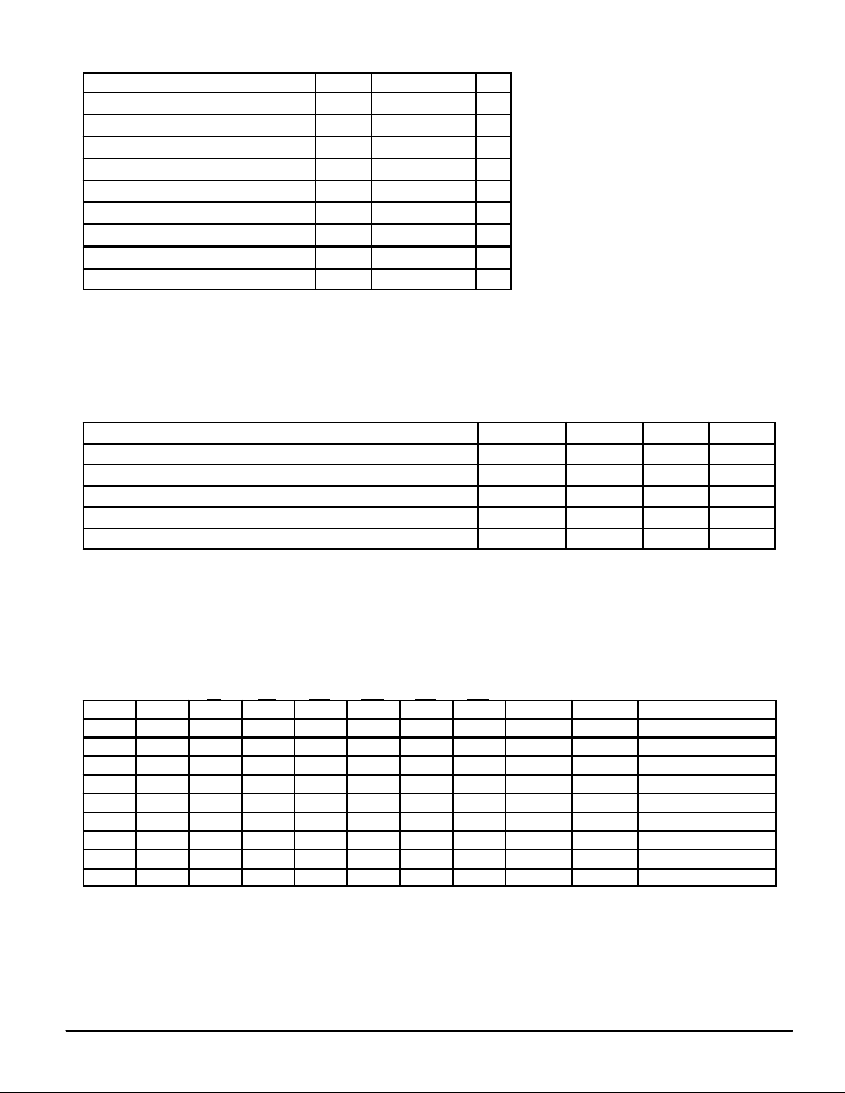
PIN ASSIGNMENTS
TOP VIEW
MCM69L737A
6543217
MCM69L819A
6543217
A
B
C
D
E
F
G
H
J
K
L
M
N
P
R
T
U
SA SA SA SA
V
DDQ
NC NC SA NC
SA SA SA SA
NC
DQc DQc VSSNC DQb
DQc
DQc
V
DQc V
DDQ
DQcDQc
DQc
DQc VSSNC DQb
V
V
V
V
DD
DDQ
DQd DQd VSSCK V
DQd V
DDQ
DQdDQd
DQd DQd VSSSA
SA SA
NC
NC
NC SA SA NC
DDQ
SBdDQdDQd
V
TDITMS
SS
SS
NC
SS
SS
DD
NC
NC
SA
V
DD
V
SS
V
DQbSSV
SS
V
G
V
DD
CK
SW
V
DD
SA
TCK
SS
SBb
V
SS
NC
SS
V
SS
V
SS
V
SS
V
SS
TDO
DQb
DQbNCSBc
V
DQa
DQaSBa
DQa
DQaSAV
DQa
NC
DD
V
V
V
V
V
DDQ
NC
NC
DQb
DQb
DDQ
DQb
DQb
DDQ
DQa
DQa
DDQ
DQa
DQa
NC
ZZ
DDQ
A
B
C
D
E
F
G
H
J
K
L
M
N
P
R
T
U
SA SA SA SA
V
DDQ
NC NC SA NC
SA SA SA SA
NC
DQb NC VSSNC DQa
DQbNC
V
NC V
DDQ
DQbNC
DQb
NC VSSNC DQa
V
V
V
V
DD
DDQ
NC DQb VSSCK V
NCDQb
DQb V
DDQ
NCDQb
NC DQb VSSSA
SA SA
NC
SA SA SA SA
NC
DDQ
V
V
TDITMS
SS
SS
NC
SS
SS
SS
DD
NC
SA
NC
V
DD
V
SS
V
NCSSV
SS
V
G
V
DD
CK
SW
V
DD
NC
TCK
SS
V
SS
V
SS
NC
SS
V
SS
V
SS
V
SS
V
SS
TDO
DQa
NCNCSBb
V
NC
DQaSBa
NC
DQaSAV
NC
NC
DD
V
V
V
V
V
DDQ
NC
NC
NC
DQa
DDQ
DQa
NC
DDQ
DQa
NC
DDQ
NC
DQa
NC
ZZ
DDQ
MCM69L737A•MCM69L819A
2
MOTOROLA FAST SRAM
MCM69L737A PIN DESCRIPTIONS
PBGA Pin Locations Symbol
4K CK Input Address, data in and control input register clock. Active high.
4L CK Input Address, data in and control input register clock. Active low.
(a) 6K, 7K, 6L, 7L, 6M, 6N, 7N, 6P, 7P
(b) 6D, 7D, 6E, 7E, 6F, 6G, 7G, 6H, 7H
(c) 1D, 2D, 1E, 2E, 2F, 1G, 2G, 1H, 2H
(d) 1K, 2K, 1L, 2L, 2M, 1N, 2N, 1P, 2P
4F G Input Output Enable: Asynchronous pin, active low.
2A, 3A, 5A, 6A, 3B, 5B, 2C, 3C,
5C, 6C, 4N, 4P, 2R, 6R, 3T, 4T, 5T
5L, 5G, 3G, 3L
(a), (b), (c), (d)
4E SS Input Synchronous Chip Enable: Registered on the rising clock edge, active
4M SW Input Synchronous Write: Registered on the rising clock edge, active low.
4U TCK Input Test Clock (JTAG).
3U TDI Input Test Data In (JT AG).
5U TDO Output Test Data Out (JTAG).
2U TMS Input T est Mode Select (JTAG).
7T ZZ Input Enables sleep mode.
4C, 2J, 4J, 6J, 4R, 3R V
1A, 7A, 1F, 7F, 1J, 7J, 1M, 7M, 1U, 7U V
3D, 5D, 3E, 5E, 3F, 5F, 3H, 5H,
3K, 5K, 3M, 5M, 3N, 5N, 3P, 5P, 5R
4A, 1B, 2B, 4B, 6B, 7B, 1C, 7C, 4D, 4G,
4H, 3J, 5J, 1R, 7R, 1T, 2T, 6T, 6U
Type Description
DQx I/O Synchronous Data I/O.
SA Input Synchronous Address Inputs: Registered on the rising clock edge.
SBx Input Synchronous Byte Write Enable: Enables writes to byte x in
DD
DDQ
V
SS
NC — No Connection: There is no connection to the chip.
Supply Core Power Supply.
Supply Output Power Supply: provides operating power for output buffers.
Supply Ground.
conjunction with the SW
low.
low.
Writes all enabled bytes.
Note: 3J and 5J are tied common.
input. Has no effect on read cycles, active
MOTOROLA FAST SRAM
MCM69L737A•MCM69L819A
3
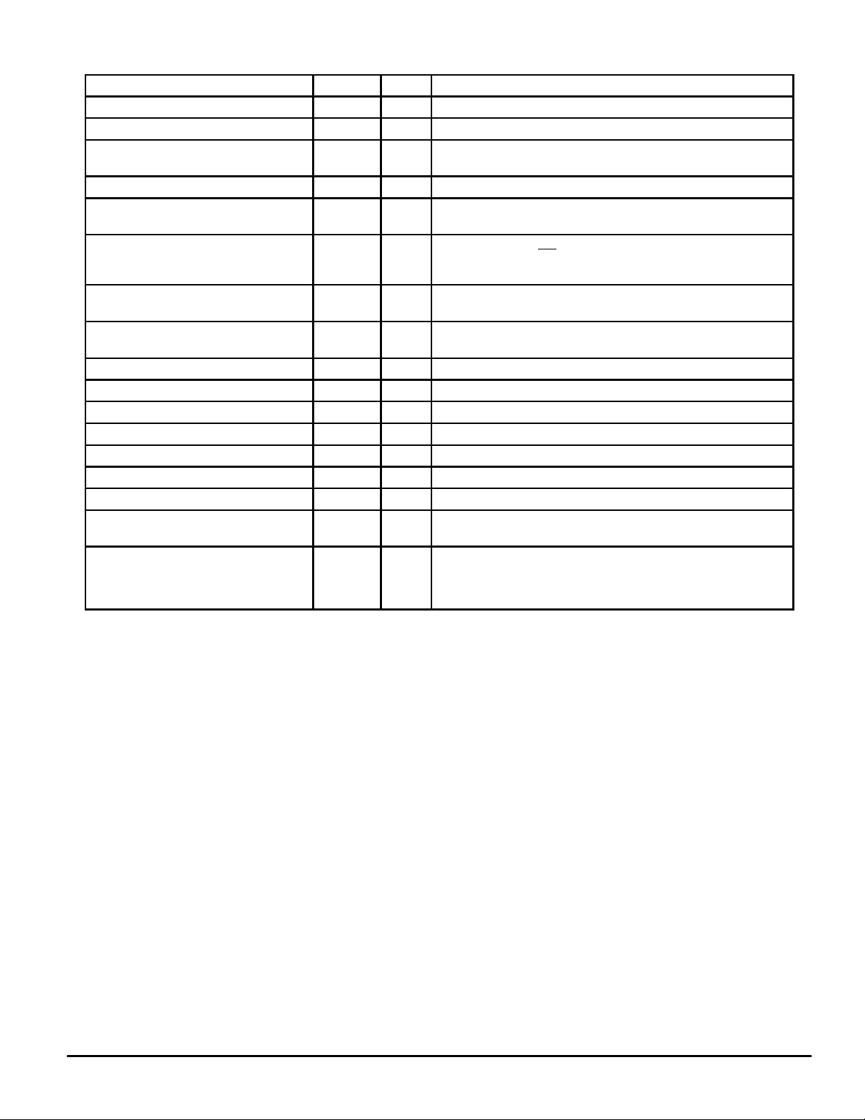
MCM69L819A PIN DESCRIPTIONS
PBGA Pin Locations Symbol
4K CK Input Address, data in and control input register clock. Active high.
4L CK Input Address, data in and control input register clock. Active low.
(a) 6D, 7E, 6F, 7G, 6H, 7K, 6L, 6N, 7P
(b) 1D, 2E, 2G, 1H, 2K, 1L, 2M, 1N, 2P
4F G Input Output Enable: Asynchronous pin, active low.
2A, 3A, 5A, 6A, 3B, 5B, 2C, 3C, 5C,
6C, 4N, 4P, 2R, 6R, 2T, 3T, 5T, 6T
5L, 3G
(a), (b)
4E SS Input Synchronous Chip Enable: Registered on the rising clock edge, active
4M SW Input Synchronous Write: Registered on the rising clock edge, active low.
4U TCK Input Test Clock (JTAG).
3U TDI Input Test Data In (JT AG).
5U TDO Output Test Data Out (JTAG).
2U TMS Input T est Mode Select (JTAG).
7T ZZ Input Enables sleep mode.
4C, 2J, 4J, 6J, 4R, 3R V
1A, 7A, 1F, 7F, 1J, 7J, 1M, 7M, 1U, 7U V
3D, 5D, 3E, 5E, 3F, 5F, 5G, 3H, 5H,
3K, 5K, 3L, 3M, 5M, 3N, 5N, 3P, 5P, 5R
4A, 1B, 2B, 4B, 6B, 7B, 1C, 7C,
2D, 4D, 7D, 1E, 6E, 2F, 1G, 4G, 6G,
2H, 4H, 7H, 3J, 5J, 1K, 6K, 2L, 7L, 6M, 2N,
7N, 1P, 6P, 1R, 7R, 1T, 4T, 6U
Type Description
DQx I/O Synchronous Data I/O.
SA Input Synchronous Address Inputs: Registered on the rising clock edge.
SBx Input Synchronous Byte Write Enable: Enables writes to byte x in
DD
DDQ
V
SS
NC — No Connection: There is no connection to the chip.
Supply Core Power Supply.
Supply Output Power Supply: provides operating power for output buffers.
Supply Ground.
conjunction with the SW
low.
low.
Writes all enabled bytes.
Note: 3J and 5J are tied common.
input. Has no effect on read cycles, active
MCM69L737A•MCM69L819A
4
MOTOROLA FAST SRAM
ABSOLUTE MAXIMUM RATINGS (Voltages Referenced to V
Rating
Core Supply Voltage V
Output Supply Voltage V
Voltage On Any Pin V
Input Current (per I/O) I
Output Current (per I/O) I
Power Dissipation (See Note 2) P
Operating Temperature T
Temperature Under Bias T
Storage Temperature T
NOTES:
1. Permanent device damage may occur if ABSOLUTE MAXIMUM RATINGS are
exceeded. Functional operation should be restricted to RECOMMENDED OPERATING CONDITIONS. Exposure to higher than recommended voltages for extended
periods of time could affect device reliability.
2. Power dissipation capability will be dependent upon package characteristics and use
environment. See enclosed thermal impedance data.
Symbol Value Unit
DD
DDQ
– 0.5 to VDD + 0.5 V
– 0.5 to VDD + 0.5 V
in
in
out
D
A
bias
stg
, See Note 1)
SS
– 0.5 to + 4.6 V
± 50 mA
± 70 mA
— W
0 to + 70 °C
– 10 to + 85 °C
– 55 to + 125 °C
This device contains circuitry to protect the
inputs against damage due to high static voltages or electric fields; however, it is advised
that normal precautions be taken to avoid
application of any voltage higher than maximum rated voltages to this high–impedance
circuit.
This BiCMOS memory circuit has been
designed to meet the dc and ac specifications
shown in the tables, after thermal equilibrium
has been established.
This device contains circuitry that will ensure
the output devices are in High–Z at power up.
PBGA PACKAGE THERMAL CHARACTERISTICS
Rating Symbol Max Unit Notes
Junction to Ambient (Still Air) R
Junction to Ambient (@200 ft/min) Single Layer Board R
Junction to Ambient (@200 ft/min) Four Layer Board R
Junction to Board (Bottom) R
Junction to Case (Top) R
NOTES:
1. Junction temperature is a function of on–chip power dissipation, package thermal resistance, mounting site (board) temperature, ambient
temperature, air flow, power dissipation of other components on the board, and board thermal resistance.
2. Per SEMI G38–87.
3. Indicates the average thermal resistance between the die and the printed circuit board.
4. Indicates the average thermal resistance between the die and the case top surfac e as measured by the cold plate method (MIL SPEC–883
Method 1012.1).
θJA
θJA
θJA
θJB
θJC
53 °C/W 1, 2
38 °C/W 1, 2
22 °C/W
14 °C/W 3
5 °C/W 4
CLOCK TRUTH TABLE
K CLK ZZ SS SW SBa SBb SBc SBd DQ (n) DQ (n+1) Mode
L – H L L H X X X X D
L – H L L L L H H H High–Z Din 0–8 Write Cycle 1st Byte
L – H L L L H L H H High–Z Din 9–17 Write Cycle 2nd Byte
L – H L L L H H L H High–Z Din 18–26 Write Cycle 3rd Byte
L – H L L L H H H L High–Z Din 27–35 Write Cycle 4th Byte
L – H L L L L L L L High–Z Din 0–35 Write Cycle All Bytes
L – H L L L H H H H High–Z High–Z Abort Write Cycle
L – H L H X X X X X High–Z X Deselect Cycle
X H X X X X X X High–Z High–Z Sleep Mode
MOTOROLA FAST SRAM
0–35 X Read Cycle All Bytes
out
MCM69L737A•MCM69L819A
5
DC OPERA TING CONDITIONS AND CHARACTERISTICS
(0°C ≤ TA ≤ 70°C, Unless Otherwise Noted)
RECOMMENDED OPERATING CONDITIONS
Parameter
Core Power Supply Voltage V
Output Driver Supply Voltage V
Active Power Supply Current (x18)
Quiescent Active Power
Supply Current
Active Standby Power Supply Current I
Quiescent Standby Power
Supply Current
Sleep Mode Power Supply Current I
NOTES:
1. All data sheet parameters specified to full range of VDD unless otherwise noted. All voltages are referenced to voltage applied to VSS bumps.
2. Supply voltage applied to VDD connections.
3. Supply voltage applied to V
4. All power supply currents measured with outputs open or deselected.
5. VDD = VDD (max), t
6. VDD = VDD (max), t
7. VDD = VDD (max), t
8. VDD = VDD (max), t
9. VDD = VDD (max), t
10. 200 mV ≥ Vin ≥ V
KHKH
KHKH
KHKH
KHKH
KHKH
DDQ
– 200 mV.
connections.
DDQ
= t
KHKH
= dc, SS
= t
KHKH
= dc, SS
= dc, SS
(min), SS
registered active.
(min), SS
registered inactive, ZZ low.
registered inactive, ZZ high.
(See Notes 1 through 4)
Typical
Symbol Min
DD
DDQ
I
(x36)
DD1
I
DD2
SB1
I
SB2
SB3
registered active, 50% read cycles.
registered inactive.
3.15 — — — 3.6 V
3.15 — — — 3.6 V
—
—
— 180 180 180 250 mA 6, 10
— 170 170 170 250 mA 7
— 150 150 150 230 mA 8, 10
— 30 30 30 50 mA 9, 10
–8.5
320
370
Typical–9Typical
320
370
–9.5
300
350
Max Unit Notes
480
550
mA 5
DC INPUT CHARACTERISTICS
Parameter Symbol Min Max Unit Notes
DC Input Logic High VIH (dc) 2.0 VDD + 0.3 V
DC Input Logic Low VIL (dc) – 0.3 0.8 V 1
Input Leakage Current I
Clock Input Leakage Current I
Clock Input Signal Voltage V
Clock Input Differential V oltage V
Clock Input Common Mode Voltage Range (See Figure 3) VCM (dc) 1.1 2.1 V 4
NOTES:
1. Inputs may undershoot to – 0.5 V (peak) for up to 20% t
2. 0 V ≤ Vin ≤ V
3. Minimum instantaneous differential input voltage required for differential input clock operation.
4. Maximum rejectable common mode input voltage variation.
DDQ
for all pins.
(e.g., 2 ns at a clock cycle time of 10 ns).
KHKH
lkg
clkg
in
(dc) 0.2 VDD + 0.6 V 3
DIF
— ± 5 µA 2
— ± 8 µA 2
– 0.3 VDD + 0.3 V
DC OUTPUT CHARACTERISTICS
Parameter Symbol Min Max Unit Notes
Output Leakage Current I
Output Low Voltage V
Output High Voltage V
NOTES:
1. IOL = 8.0 mA.
2. IOH = – 8.0 mA.
CAPACITANCE (f = 1.0 MHz, dV = 3.0 V, 0°C ≤ T
Characteristic
Input Capacitance C
Input/Output Capacitance C
CK, CK Capacitance C
≤ 70°C, Periodically Sampled Rather Than 100% Tested)
A
lkg
OL
OH
MCM69L737A•MCM69L819A
6
– 1.0 1.0 µA
— 0.4 V 1
2.4 — V 2
Symbol Typ Max Unit
in
I/O
CK
4 5 pF
7 8 pF
4 5 pF
MOTOROLA FAST SRAM
 Loading...