

Motorola MCM67D709FN16 Datasheet
MCM67D709
1
MOTOROLA FAST SRAM
128K x 9 Bit Synchronous
Dual I/O Fast Static RAM
The MCM67D709 is a 1,179,648 bit synchronous static random access
memory organized as 131,072 words of 9 bits, fabricated using Motorola’s
high–performance silicon–gate BiCMOS technology. The device integrates a
128K x 9 SRAM core with advanced peripheral circuitry consisting of address
registers, two sets of input data registers and two sets of output latches. This
device has increased output drive capability supported by multiple power pins.
Asynchronous inputs include the processor output enable (POE
) and the
system output enable (SOE
).
The address inputs (A0 – A16) are synchronous and are registered on the
falling edge of clock (K). Write enable (W), processor input enable (PIE) and
system input enable (SIE
) are registered on the rising edge of clock (K). Writes
to the RAM are self–timed.
All data inputs/outputs, PDQ0 – PDQ7, SDQ0 – SDQ7, PDQP, and SDQP
have input data registers triggered by the rising edge of the clock. These pins also
have three–state output latches which are transparent during the high
level of the clock and latched during the low level of the clock.
This device has a special feature which allows data to be passed through the
RAM between the system and processor ports in either direction. This streaming
is accomplished by latching in data from one port and asynchronously output
enabling the other port. It is also possible to write to the RAM while streaming.
The MCM67D709’s dual I/Os can be used in x9 separate I/O applications.
Common I/Os PDQ0 – 7, PDQP and SDQ0 – 7, SDQP can be treated as either
inputs (D) or outputs (Q) depending on the state of the control pins. In order to
dedicate PDQ0 – 7, PDQP as data (D) inputs and SDQ0 – 7, SDQP as outputs
(Q), tie SIE
and POE high. SOE becomes the asynchronous G for the outputs.
PIE
will need to track W for proper write/read operations.
This device is ideally suited for pipelined systems and systems with multiple
data buses and multi–processing systems, where a local processor has a bus
isolated from a common system bus.
• Single 5 V ± 5% Power Supply
• 88110/88410 Compatibility: –16/60 MHz, –20/50 MHz
• Self–Timed Write Cycles
• Clock Controlled Output Latches
• Address and Data Input Registers
• Common Data Inputs and Data Outputs
• Dual I/O for Separate Processor and Memory Buses
• Separate Output Enable Controlled Three–State Outputs
• 3.3 V I/O Compatible
• High Board Density 52 Lead PLCC Package
• Can be used as Separate I/O x9 SRAM
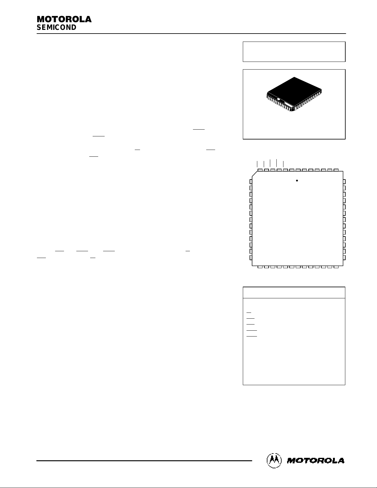
PIN ASSIGNMENTS
10
9
8
12
11
15
14
13
17
16
20
19
18
37
38
34
35
36
42
43
39
40
41
45
46
44
21 22 23 24 25 26 2728 29 30 31 3233
7 6 5 4 3 2 1 52 51 50 49 4847
A16
A15
PDQ7
SDQ7
V
SS
PDQ5
V
CC
PDQ3
SDQ3
V
SS
PDQ1
SDQ1
SDQ5
PDQP
SDQP
V
SS
PDQ6
SDQ6
V
CC
PDQ4
SDQ4
PDQ2
SDQ2
V
SS
PDQ0
SDQ0
SIE
PIE
SOE
POEWEK
VCCVSSNCA6A4
A2
V
SS
V
CC
A14
A13
A12
A11
A10
A9A8A7A5A3
A1 A0
All power supply and ground pins must be
connected for proper operation of the
device.
PIN NAMES
A0 – A16 Address Inputs. . . . . . . . . . . . . . .
K Clock Input. . . . . . . . . . . . . . . . . . . . . . . . .
W
Write Enable. . . . . . . . . . . . . . . . . . . . . . .
PIE
Processor Input Enable. . . . . . . . . . . . .
SIE
System Input Enable. . . . . . . . . . . . . . .
POE Processor Output Enable. . . . . . . . . .
SOE
System Output Enable. . . . . . . . . . . . .
PDQ0 – PDQ7 Processor Data I/O. . . . . . .
PDQP Processor Data Parity. . . . . . . . . . .
SDQ0 – SDQ7 System Data I/O. . . . . . . . .
SDQP System Data Parity. . . . . . . . . . . . .
V
CC
+ 5 V Power Supply. . . . . . . . . . . . . . .
V
SS
Ground. . . . . . . . . . . . . . . . . . . . . . . . . .
NC No Connection. . . . . . . . . . . . . . . . . . . .
Order this document
by MCM67D709/D
MOTOROLA
SEMICONDUCTOR TECHNICAL DATA
MCM67D709
FN PACKAGE
PLASTIC
CASE 778–02
REV2
5/95
Motorola, Inc. 1994
MCM67D709
2
MOTOROLA FAST SRAM
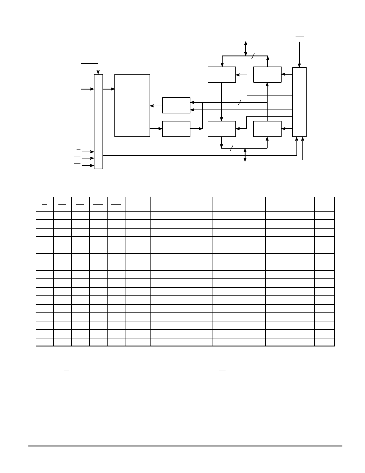
BLOCK DIAGRAM
K
9
9
9
REGISTER
CONTROL
WRITE
DRIVER
A0 – A16
W
PIE
SIE
POE
SOE
128K x 9 ARRAY
DATA
REGISTER
DATA
REGISTER
DATA
LATCH
DATA
LATCH
SENSE
AMPLIFIER
SDQ0 – SDQ7, SDQP
PDQ0 – PDQ7, PDQP
FUNCTIONAL TRUTH TABLE (See Notes 1 and 2)
W
PIE SIE POE SOE Mode
Memory Subsystem
Cycle
PDQ0 – PDQ7,
PDQP Output
SDQ0 – SDQ7,
SDQP Output
Notes
1 1 1 0 1 Read Processor Read Data Out High–Z 3
1 1 1 1 0 Read Copy Back High–Z Data Out 3
1 1 1 0 0 Read Dual Bus Read Data Out Data Out 3
1 X X 1 1 Read NOP High–Z High–Z
X 0 0 X X N/A NOP High–Z High–Z 2, 4
0 0 1 1 1 Write Processor Write Hit Data In High–Z 2, 5
0 1 0 1 1 Write Allocate High–Z Data In 2, 5
0 0 1 1 0 Write Write Through Data In Stream Data 2, 6
0 1 0 0 1 Write Allocate With Stream Stream Data Data In 2, 6
1 0 1 1 0 N/A Cache Inhibit Write Data In Stream Data 2, 6
1 1 0 0 1 N/A Cache Inhibit Read Stream Data Data In 2, 6
0 1 1 X X N/A NOP High–Z High–Z 4
X 0 1 0 0 N/A Invalid Data In Stream 2, 7
X 0 1 0 1 N/A Invalid Data In High–Z 2, 7
X 1 0 0 0 N/A Invalid Stream Data In 2, 7
X 1 0 1 0 N/A Invalid High–Z Data In 2, 7
NOTES:
1. A ‘0’ represents an input voltage ≤ VIL and a ‘1’ represents an input voltage ≥ VIH. All inputs must satisfy the specified setup and hold times
for the falling or rising edge of K. Some entries in this truth table represent latched values. Other possible combinations of control inputs not
covered by this note or the table above are not supported and the RAMs behavior is not specified.
2. If either IE
signal is sampled low on the rising edge of clock, the corresponding OE is a don’t care, and the corresponding outputs are
High–Z.
3. A read cycle is defined as a cycle where data is driven on the internal data bus by the RAM.
4. No RAM cycle is performed.
5. A write cycle is defined as a cycle where data is driven onto the internal data bus through one of the data I/O ports (PDQ0 – PDQ7 and
PDQP or SDQ0 – SDQ7 and SPDQ), and written into the RAM.
6. Data is driven on the internal data bus by one I/O port through its data input register and latched into the data output latch of the other
I/O port.
7. Data contention will occur.
MCM67D709
3
MOTOROLA FAST SRAM
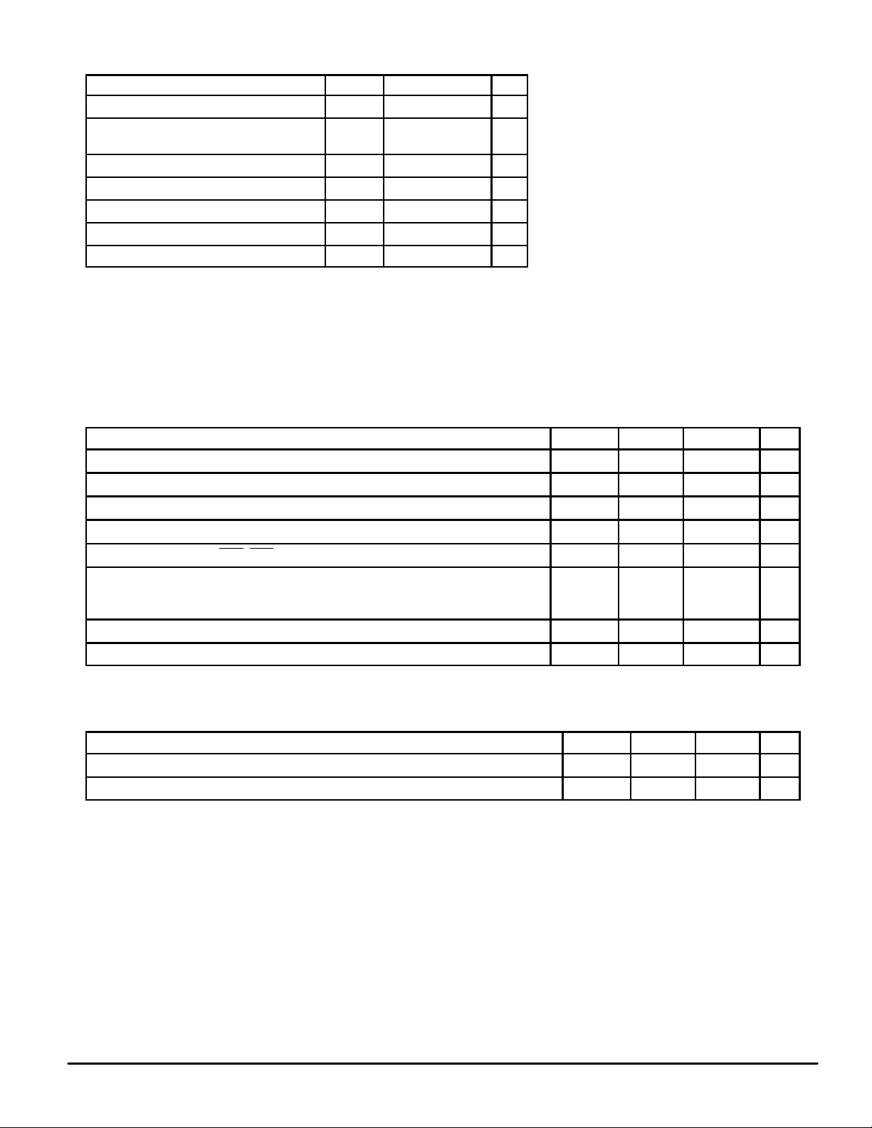
ABSOLUTE MAXIMUM RATINGS (Voltages Referenced to V
SS
= 0 V)
Rating
Symbol Value Unit
Power Supply V
CC
– 0.5 to + 7.0 V
Voltage Relative to VSS for Any Pin
Except V
CC
Vin, V
out
– 0.5 to VCC + 0.5 V
Output Current (per I/O) I
out
± 30 mA
Power Dissipation P
D
2.0 W
Temperature Under Bias T
bias
– 10 to + 85 °C
Operating Temperature T
A
0 to +70 °C
Storage Temperature T
stg
– 55 to + 125 °C
NOTE: Permanent device damage may occur if ABSOLUTE MAXIMUM RATINGS are
exceeded. Functional operation should be restricted to RECOMMENDED
OPERATING CONDITIONS. Exposure to higher than recommended voltages for
extended periods of time could affect device reliability.
DC OPERATING CONDITIONS AND CHARACTERISTICS
(VCC = 5.0 V ± 5%, TA = 0 to + 70°C, Unless Otherwise Noted)
RECOMMENDED OPERATING CONDITIONS AND SUPPLY CURRENTS
(Voltages referenced to VSS = 0 V)
Parameter
Symbol Min Max Unit
Supply Voltage (Operating Voltage Range) V
CC
4.75 5.25 V
Input High Voltage V
IH
2.2 VCC + 0.3** V
Input Low Voltage V
IL
– 0.5* 0.8 V
Input Leakage Current (All Inputs, Vin = 0 to VCC) I
lkg(I)
— ± 1.0 µA
Output Leakage Current (POE, SOE = VIH) I
lkg(O)
— ± 1.0 µA
AC Supply Current (All Inputs = VIL or VIH,VIL = 0.0 V and VIH ≥ 3.0 V,
I
out
= 0 mA, Cycle Time ≥ t
KHKH
min) MCM67D709–16: t
KHKH
= 16 ns
MCM67D709–20: t
KHKH
= 20 ns
I
CCA
—
—
280
260
mA
Output Low Voltage (IOL = + 8.0 mA) V
OL
— 0.4 V
Output High Voltage (IOH = – 4.0 mA) V
OH
2.4 3.3 V
*VIL (min) = – 0.5 V dc; VIL (min) = – 2.0 V ac (pulse width ≤ 20 ns) for I ≤ 20.0 mA.
**VIH (max) = VCC + 0.3 V dc; VIH (max) = VCC + 2.0 V ac (pulse width ≤ 20 ns) for I ≤ 20.0 mA.
CAPACITANCE (f = 1.0 MHz, dV = 3.0 V, T
A
= 25°C, Periodically Sampled Rather Than 100% Tested)
Parameter
Symbol Typ Max Unit
Input Capacitance (All Pins Except I/Os) C
in
5 6 pF
Input/Output Capacitance (PDQ0 – PDQ7, SDQ0 – SDQ7, PDQP, SDQP) C
out
6 7 pF
This device contains circuitry to protect the
inputs against damage due to high static voltages or electric fields; however, it is advised
that normal precautions be taken to avoid
application of any voltage higher than maximum rated voltages to this high–impedance
circuit.
MCM67D709
4
MOTOROLA FAST SRAM
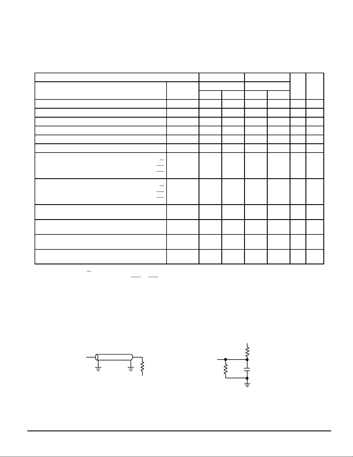
AC OPERATING CONDITIONS AND CHARACTERISTICS
(VCC = 5.0 V ± 5%, TA = 0 to + 70°C, Unless Otherwise Noted)
Input Timing Measurement Reference Level 1.5 V. . . . . . . . . . . . . . .
Input Pulse Levels 0 to 3.0 V. . . . . . . . . . . . . . . . . . . . . . . . . . . . . . . . .
Input Rise/Fall Time 3 ns. . . . . . . . . . . . . . . . . . . . . . . . . . . . . . . . . . . .
Output Measurement Timing Level 1.5 V. . . . . . . . . . . . . . . . . . . . . . .
Output Load See Figure 1A Unless Otherwise Noted. . . . . . . . . . . .
READ CYCLE (See Note 1)
Processor Frequency
60 MHz 50 MHz
MCM67D709–16 MCM67D709–20
Parameter Symbol Min Max Min Max Unit Notes
Read Cycle Time Clock High to Clock High t
KHKH
16 — 20 — ns 1, 2
Clock Low Pulse Width t
KLKH
5 — 5 — ns
Clock High Pulse Width t
KHKL
7 — 7 — ns
Clock High to Output Valid t
KHQV
— 6 — 7.5 ns 3
Clock (K) High to Output Low Z After Write t
KHQX1
0 — 0 — ns
Output Hold from Clock High t
KHQX2
2 — 3 — ns 3, 4
Setup Times: A
W
PIE
SIE
t
AVKL
t
WHKH
t
PIEHKH
t
SIEHKH
2
2
2
2
— 2
2
2
2
— ns
Hold Times: A
W
PIE
SIE
t
KLAX
t
KHWX
t
KHPIEX
t
KHSIEX
2
2
2
2
— 2
2
2
2
— ns
Output Enable High to Q High–Z t
POEHQZ
t
SOEHQZ
0 6 0 8 ns 4
Output Hold from Output Enable High t
POEHQX
t
SOEHQX
2 — 5 — ns 4
Output Enable Low to Q Active t
POELQX
t
SOELQX
0 — 0 — ns 4
Output Enable Low to Output Valid t
POELQV
t
SOELQV
— 5 — 6 ns
NOTES:
1. A read is defined by W
high for the setup and hold times.
2. All read cycle timing is referenced from K, SOE
, or POE.
3. K must be at a high level for outputs to transition.
4. Transition is measured ± 500 mV from steady–state voltage with output load of Figure 1B. This parameter is sampled and not 100% tested.
At any given voltage and temperature, t
POEHQZ
is less than t
POELQX
for a given device, and t
SOEHQZ
is less than t
SOELQX
for
a given device.
AC SPEC LOADS
Figure 1B
5 pF
+ 5 V
OUTPUT
255
Ω
480
Ω
Figure 1A
OUTPUT
Z0 = 50
Ω
RL = 50
Ω
VL = 1.5 V
 Loading...