

Motorola MCM67C618AFN7, MCM67C618AFN5 Datasheet
MOTOROLA
SEMICONDUCTOR TECHNICAL DATA
64K x 18 Bit BurstRAM
Synchronous Fast Static RAM
With Burst Counter and Registered Outputs
The MCM67C618A is a 1,179,648 bit synchronous static random access
memory designed to provide a burstable, high–performance, secondary cache
for the i486 and Pentium microprocessors. It is organized as 65,536 words
of 18 bits, fabricated with Motorola’s high–performance silicon–gate BiCMOS
technology. The device integrates input registers, a 2–bit counter, high speed
SRAM, and high drive registered output drivers onto a single monolithic circuit
for reduced parts count implementation of cache data RAM applications. Synchronous design allows precise cycle control with the use of an external clock (K).
BiCMOS circuitry reduces the overall power consumption of the integrated
functions for greater reliability .
Addresses (A0 – A15), data inputs (D0 – D17), and all control signals
except output enable (G
triggered noninverting registers.
This device contains output registers for pipeline operations. At the rising edge of K, the RAM provides the output data from the previous cycle.
Output enable (G
ity.
Burst can be initiated with either address status processor (ADSP
dress status cache controller (ADSC
dresses can be generated internally by the MCM67C618A (burst
sequence imitates that of the i486 and Pentium) and controlled by the burst
address advance (ADV
tailed information on burst controls.
Write cycles are internally self–timed and are initiated by the rising edge
of the clock (K) input. This feature eliminates complex off–chip write pulse
generation and provides increased flexibility for incoming signals.
Dual write enables (L W
able bytes. LW
controls DQ0 – DQ8 (the lower bits), while UW controls
DQ9 – DQ17 (the upper bits).
This device is ideally suited for systems that require wide data bus
widths and cache memory . See Figure 2 for applications information.
• Single 5 V
± 5% Power Supply
• Fast Access Time/Fast Cycle Time = 5 ns/100 MHz, 7 ns/80 MHz
• Byte Writeable via Dual Write Enables
• Internal Input Registers (Address, Data, Control)
• Output Registers for Pipelined Applications
• Internally Self–Timed Write Cycle
• ADSP
, ADSC, and ADV Burst Control Pins
• Asynchronous Output Enable Controlled Three–State Outputs
• Common Data Inputs and Data Outputs
• 3.3 V I/O Compatible
• High Board Density 52–Lead PLCC Package
) are clock (K) controlled through positive–edge–
) is asynchronous for maximum system design flexibil-
) or ad-
) input pins. Subsequent burst ad-
) input pin. The following pages provide more de-
and UW) are provided to allow individually write-
DQ9
DQ10
V
CC
V
SS
DQ11
DQ12
DQ13
DQ14
V
SS
V
CC
DQ15
DQ16
DQ17
Order this document
by MCM67C618A/D
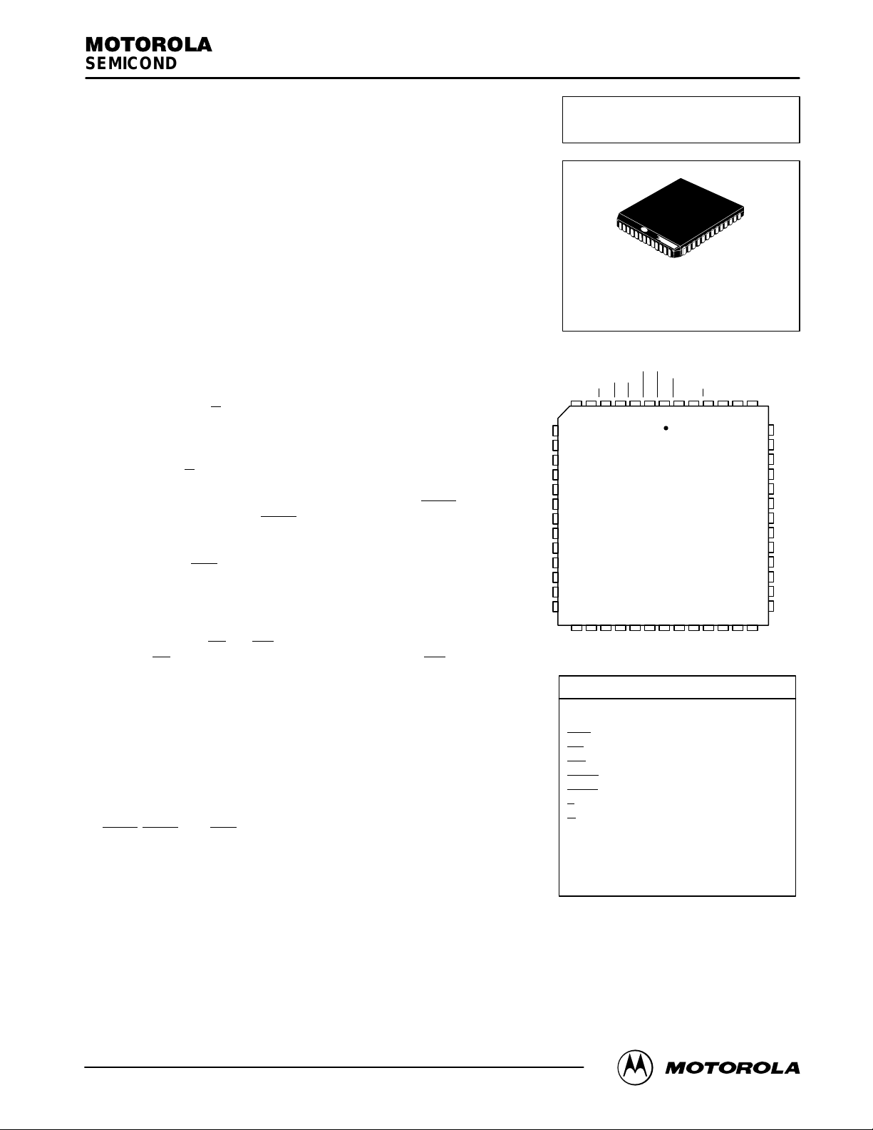
MCM67C618A
FN PACKAGE
PLASTIC
CASE 778–02
PIN ASSIGNMENTS
A6A7E
7 654 321525150494847
8
9
10
11
12
13
14
15
16
17
18
19
20
21 22 23 24 25 26 2728 29 30 31 3233
A5
UW
A4A3A2
LW
A1
ADSP
ADSC
A0
SS
V
PIN NAMES
A0 – A15 Address Inputs. . . . . . . . . . . . . . . .
K Clock. . . . . . . . . . . . . . . . . . . . . . . . . . . . . . .
ADV
LW
UW
ADSC
ADSP
E
G
DQ0 – DQ17 Data Input/Output. . . . . . . . . .
V
CC
V
SS
NC No Connection. . . . . . . . . . . . . . . . . . . . .
All power supply and ground pins must be
connected for proper operation of the device.
Burst Address Advance. . . . . . . . . . . .
Lower Byte Write Enable. . . . . . . . . . . .
Upper Byte Write Enable. . . . . . . . . . . .
Controller Address Status. . . . . . . . .
Processor Address Status. . . . . . . . .
ADV
CC
V
+ 5 V Power Supply. . . . . . . . . . . . . . . .
K
A15
G
A8A9A10
A13
A14
Chip Enable. . . . . . . . . . . . . . . . . . . . . . . . .
Output Enable. . . . . . . . . . . . . . . . . . . . . .
A12
Ground. . . . . . . . . . . . . . . . . . . . . . . . . .
46
45
44
43
42
41
40
39
38
37
36
35
34
A11
DQ8
DQ7
DQ6
V
CC
V
SS
DQ5
DQ4
DQ3
DQ2
V
SS
V
CC
DQ1
DQ0
BurstRAM is a trademark of Motorola, Inc.
i486 and Pentium are trademarks of Intel Corp.
REV 2
11/5/96
Motorola, Inc. 1996
MOTOROLA FAST SRAM
MCM67C618A
1
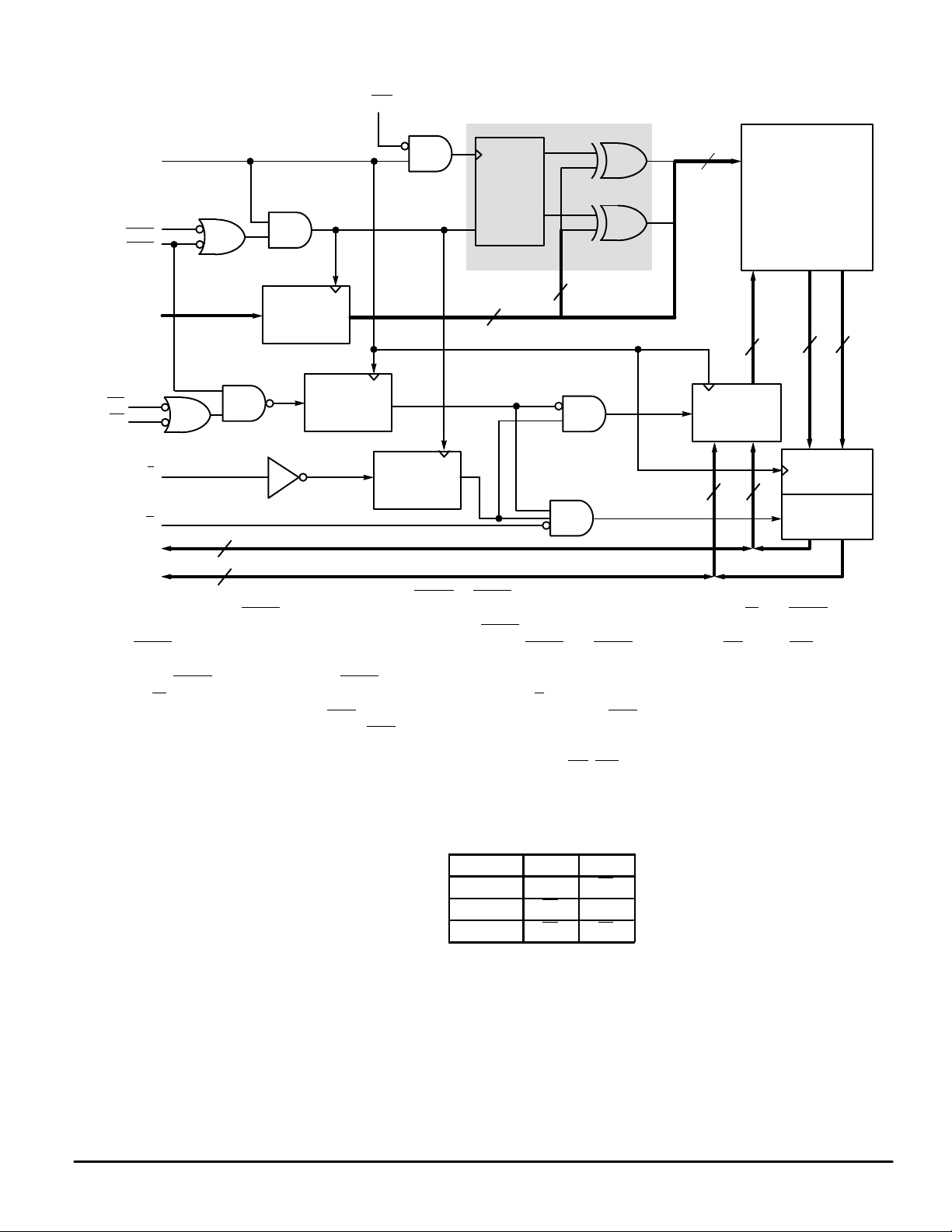
BLOCK DIAGRAM (See Note)
ADV
K
ADSC
ADSP
A0 – A15
UW
LW
E
G
DQ0 – DQ8
DQ9 – DQ17
NOTE: All registers are positive–edge triggered. The ADSC or ADSP signals control the duration of the burst and the start of the
9
9
next burst. When ADSP
ADDRESS
REGISTER
WRITE
REGISTER
ENABLE
REGISTER
is sampled low, any ongoing burst is interrupted and a read (independent of W and ADSC) is per-
CLR
BURST LOGIC
Q0
BINARY
COUNTER
Q1
A1 – A0
16
A0
A1
2
A2 – A15
A0
′
INTERNAL
ADDRESS
16
18
DATA–IN
REGISTERS
9 9
64K x 18
MEMORY
ARRAY
9
9
DATA–OUT
REGISTERS
OUTPUT
BUFFER
formed using the new external address. Alternatively , an ADSP–initiated two cycle WRITE can be performed by asserting
and a valid address on the first cycle, then negating both ADSP and ADSC and asserting LW and/or UW with valid
ADSP
data on the second cycle (see Single Write cycle in WRITE CYCLES timing diagram).
When ADSC
on W
is sampled low (and ADSP is sampled high), any ongoing burst is interrupted and a read or write (dependent
) is performed using the new external address. Chip enable (E) is sampled only when a new base address is loaded.
After the first cycle of the burst, ADV controls subsequent burst cycles. When ADV is sampled low, the internal address is
advanced prior to the operation. When ADV
is sampled high, the internal address is not advanced, thus inserting a wait state
into the burst sequence accesses. Upon completion of a burst, the address will wrap around to its initial state. See BURST
SEQUENCE TABLE. W rite refers to either or both byte write enables (LW
, UW).
MCM67C618A
2
BURST SEQUENCE TABLE (See Note)
External Address A15 – A2
1st Burst Address A15 – A2 A1 A0
2nd Burst Address A15 – A2 A1 A0
3rd Burst Address A15 – A2 A1 A0
NOTE: The burst wraps around to its initial state upon completion.
A1 A0
MOTOROLA FAST SRAM
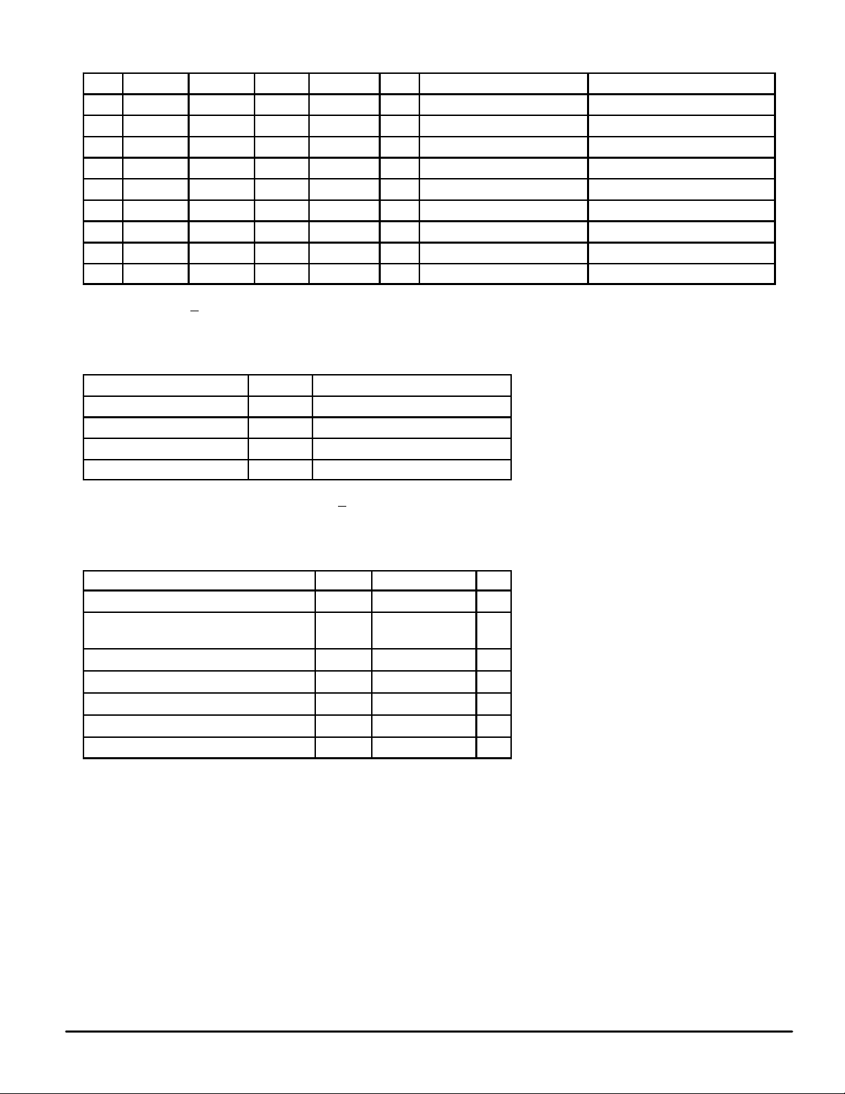
SYNCHRONOUS TRUTH TABLE (See Notes 1, 2, and 3)
E
H L X X X L–H N/A Deselected
H X L X X L–H N/A Deselected
X H H L L L–H Next Address Write Cycle, Continue Burst
X H H L H L–H Next Address Read Cycle, Continue Burst
X H H H L L–H Current Address Write Cycle, Suspend Burst
X H H H H L–H Current Address Read Cycle, Suspend Burst
NOTES:
1. X means Don’t Care.
2. All inputs except G
3. Wait states are inserted by suspending burst.
ADSP ADSC ADV UW or LW K Address Used Operation
L L X X X L–H External Address Read Cycle, Begin Burst
L H L X L L–H External Address Write Cycle, Begin Burst
L H L X H L–H External Address Read Cycle, Begin Burst
must meet setup and hold times for the low–to–high transition of clock (K).
ASYNCHRONOUS TRUTH TABLE (See Notes 1 and 2)
Operation
Read L Data Out
Read H High–Z
Write X High–Z — Data In
Deselected X High–Z
NOTES:
1. X means Don’t Care.
2. For a write operation following a read operation, G
required setup time and held high through the input data hold time.
G I/O Status
must be high before the input data
ABSOLUTE MAXIMUM RATINGS (Voltages Referenced to V
Rating
Power Supply Voltage V
Voltage Relative to VSS for Any
Pin Except V
Output Current (per I/O) I
Power Dissipation P
Temperature Under Bias T
Operating Temperature T
Storage Temperature T
NOTE: Permanent device damage may occur if ABSOLUTE MAXIMUM RATINGS are
CC
exceeded. Functional operation should be restricted to RECOMMENDED OPERATING CONDITIONS. Exposure to higher than recommended voltages for
extended periods of time could affect device reliability.
Symbol Value Unit
CC
Vin, V
– 0.5 to VCC + 0.5 V
out
out
D
bias
A
stg
= 0 V)
SS
– 0.5 to + 7.0 V
± 30 mA
1.6 W
– 10 to + 85 °C
0 to +70 °C
– 55 to + 125 °C
This device contains circuitry to protect the
inputs against damage due to high static voltages or electric fields; however, it is advised
that normal precautions be taken to avoid
application of any voltage higher than maximum rated voltages to this high–impedance
circuit.
This BiCMOS memory circuit has been
designed to meet the dc and ac specifications
shown in the tables, after thermal equilibrium
has been established.
This device contains circuitry that will ensure
the output devices are in High–Z at power up.
MOTOROLA FAST SRAM
MCM67C618A
3
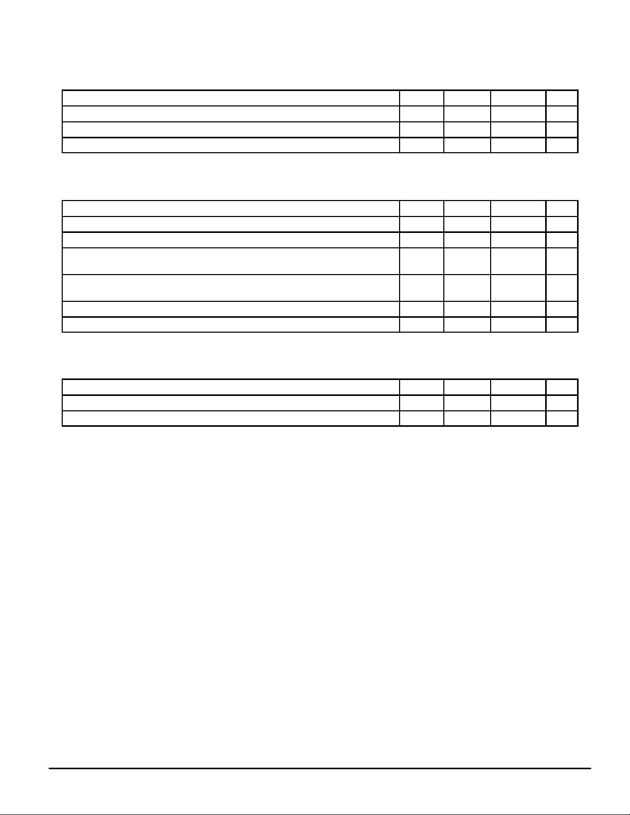
DC OPERA TING CONDITIONS AND CHARACTERISTICS
(VCC = 5.0 V ± 5%, TA = 0 to + 70°C, Unless Otherwise Noted)
RECOMMENDED OPERATING CONDITIONS
Parameter
Supply Voltage (Operating Voltage Range) V
Input High Voltage V
Input Low Voltage V
*VIL (min) = – 0.5 V dc; VIL (min) = – 2.0 V ac (pulse width ≤ 20 ns) for I ≤ 20.0 mA.
**VIH (max) = VCC + 0.3 V dc; VIH (max) = VCC + 2.0 V ac (pulse width ≤ 20 ns) for I ≤ 20.0 mA.
(Voltages Referenced to VSS = 0 V)
Symbol Min Max Unit
CC
IH
IL
4.75 5.25 V
2.2 VCC + 0.3** V
– 0.5* 0.8 V
DC CHARACTERISTICS
Parameter Symbol Min Max Unit
Input Leakage Current (All Inputs, Vin = 0 to VCC) I
Output Leakage Current (G = VIH) I
AC Supply Current (G = VIH, E = VIL, I
VIL = 0.0 V and VIH ≥ 3.0 V, Cycle Time ≥ t
AC Standby Current (E = VIH, I
VIL = 0.0 V and VIH ≥ 3.0 V, Cycle Time ≥ t
Output Low Voltage (IOL = + 8.0 mA) V
Output High Voltage (IOH = – 4.0 mA) V
NOTE: Good decoupling of the local power supply should always be used. DC characteristics are guaranteed for all possible i486 and Pentium
bus cycles.
out
CAPACITANCE (f = 1.0 MHz, dV = 3.0 V, T
Input Capacitance (All Pins Except DQ0 – DQ17) C
Input/Output Capacitance (DQ0 – DQ17) C
= 0 mA, All Inputs = VIL or VIH,
out
= 0 mA, All Inputs = VIL and V
Parameter
min)
KHKH
min)
KHKH
= 25°C, Periodically Sampled Rather Than 100% Tested)
A
IH,
lkg(I)
lkg(O)
I
CCA5
I
CCA7
I
SB1
OL
OH
Symbol Typ Max Unit
in
I/O
— ± 1.0 µA
— ± 1.0 µA
— 310
290
— 95 mA
— 0.4 V
2.4 3.3 V
4 5 pF
6 8 pF
mA
MCM67C618A
4
MOTOROLA FAST SRAM
 Loading...