

查询MCM67B618A供应商
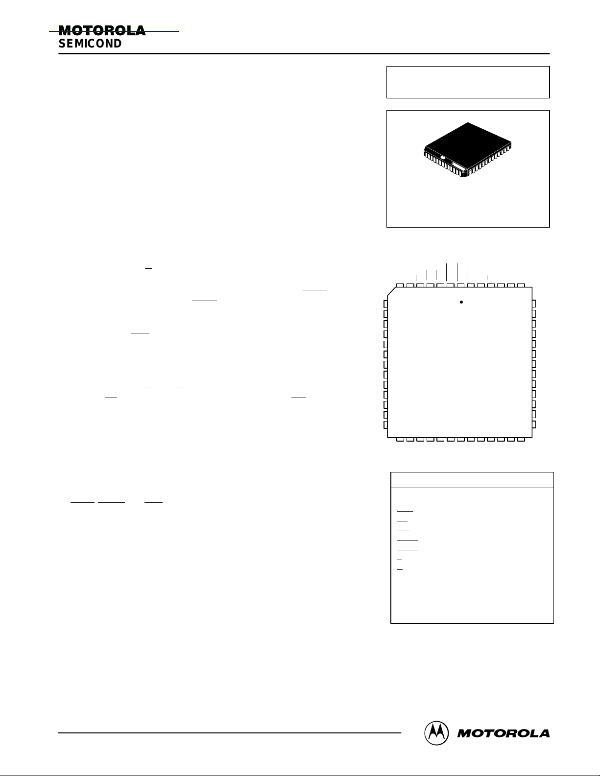
MOTOROLA
SEMICONDUCTOR TECHNICAL DATA
64K x 18 Bit BurstRAM
Synchronous Fast Static RAM
With Burst Counter and Self–Timed Write
The MCM67B618A is a 1,179,648 bit synchronous fast static random access
memory designed to provide a burstable, high–performance, secondary cache
for the i486 and Pentium microprocessors. It is organized as 65,536 words
of 18 bits. The device integrates input registers, a 2–bit counter, high speed
SRAM, and high drive capability outputs onto a single monolithic circuit for reduced parts count implementation of cache data RAM applications. Synchronous design allows precise cycle control with the use of an external clock (K).
BiCMOS circuitry reduces the overall power consumption of the integrated functions for greater reliability .
Addresses (A0 – A15), data inputs (D0 – D17), and all control signals
except output enable (G
triggered noninverting registers.
Bursts can be initiated with either address status processor (ADSP
address status cache controller (ADSC
addresses can be generated internally by the MCM67B618A (burst
sequence imitates that of the i486 and Pentium) and controlled by the burst
address advance (ADV
tailed information on burst controls.
Write cycles are internally self–timed and are initiated by the rising edge
of the clock (K) input. This feature eliminates complex off–chip write pulse
generation and provides increased flexibility for incoming signals.
Dual write enables (L W
able bytes. LW
controls DQ0 – DQ8 (the lower bits), while UW controls
DQ9 – DQ17 (the upper bits).
This device is ideally suited for systems that require wide data bus
widths and cache memory . See Figure 2 for applications information.
• Single 5 V
± 5% Power Supply
• Fast Access Times: 9/10/12 ns Max
• Byte Writeable via Dual Write Enables
• Internal Input Registers (Address, Data, Control)
• Internally Self–Timed Write Cycle
• ADSP
, ADSC, and ADV Burst Control Pins
• Asynchronous Output Enable Controlled Three–State Outputs
• Common Data Inputs and Data Outputs
• 3.3 V I/O Compatible
• High Board Density 52–Lead PLCC Package
) are clock (K) controlled through positive–edge–
) or
) input pins. Subsequent burst
) input pin. The following pages provide more de-
and UW) are provided to allow individually write-
DQ9
DQ10
V
CC
V
SS
DQ11
DQ12
DQ13
DQ14
V
SS
V
CC
DQ15
DQ16
DQ17
Order this document
by MCM67B618A/D
MCM67B618A
FN PACKAGE
PLASTIC
CASE 778–02
PIN ASSIGNMENTS
A6A7E
7 654 321525150494847
8
9
10
11
12
13
14
15
16
17
18
19
20
21 22 23 24 25 26 27 28 29 30 31 32 33
A4A3A2
A5
UW
LW
A1
ADSC
A0
SS
V
ADSP
PIN NAMES
A0 – A15 Address Inputs. . . . . . . . . . . . . . . .
K Clock. . . . . . . . . . . . . . . . . . . . . . . . . . . . . . .
ADV
LW
UW
ADSC
ADSP
E
G
DQ0 – DQ17 Data Input/Output. . . . . . . . . .
V
CC
V
SS
NC No Connection. . . . . . . . . . . . . . . . . . . . .
All power supply and ground pins must be
connected for proper operation of the device.
Lower Byte Write Enable. . . . . . . . . . . .
Upper Byte Write Enable. . . . . . . . . . . .
Controller Address Status. . . . . . . . .
Processor Address Status. . . . . . . . .
Burst Address Advance. . . . . . . . . . . .
ADV
CC
V
+ 5 V Power Supply. . . . . . . . . . . . . . . .
K
A15
G
A8A9A10
A13
A14
Chip Enable. . . . . . . . . . . . . . . . . . . . . . . . .
Output Enable. . . . . . . . . . . . . . . . . . . . . .
A12
46
45
44
43
42
41
40
39
38
37
36
35
34
A11
Ground. . . . . . . . . . . . . . . . . . . . . . . . . .
DQ8
DQ7
DQ6
V
CC
V
SS
DQ5
DQ4
DQ3
DQ2
V
SS
V
CC
DQ1
DQ0
BurstRAM is a trademark of Motorola, Inc.
i486 and Pentium are trademarks of Intel Corp.
REV 2
11/5/96
Motorola, Inc. 1996
MOTOROLA FAST SRAM
MCM67B618A
1
BLOCK DIAGRAM (See Note)
K
ADSC
ADSP
A0 – A15
UW
LW
E
G
DQ0 – DQ8
DQ9 – DQ17
ADV
CLR
ADDRESS
REGISTER
WRITE
REGISTER
ENABLE
REGISTER
9
9
BINARY
16
BURST LOGIC
Q0
A0
COUNTER
Q1
A1
A1 – A0
2
A2 – A15
A0
A1
′
′
INTERNAL
ADDRESS
16
DATA–IN
REGISTERS
9 9
18
64K
×
18
MEMORY
ARRAY
9
OUTPUT
BUFFER
9
NOTE: All registers are positive–edge triggered. The ADSC or ADSP signals control the duration of the burst and the start of the
next burst. When ADSP
is sampled low, any ongoing burst is interrupted and a read (independent of W and ADSC) is per-
formed using the new external address. Alternatively , an ADSP–initiated two cycle WRITE can be performed by asserting
and a valid address on the first cycle, then negating both ADSP and ADSC and asserting LW and/or UW with valid
ADSP
data on the second cycle (see Single Write Cycle in WRITE CYCLES timing diagram).
When ADSC
on W
After the first cycle of the burst, ADV
is advanced prior to the operation. When ADV
is sampled low (and ADSP is sampled high), any ongoing burst is interrupted and a read or write (dependent
) is performed using the new external address. Chip enable (E) is sampled only when a new base address is loaded.
controls subsequent burst cycles. When ADV is sampled low, the internal address
is sampled high, the internal address is not advanced, thus inserting a wait
state into the burst sequence accesses. Upon completion of a burst, the address will wrap around to its initial state. See
BURST SEQUENCE TABLE. Write refers to either or both byte write enables (L W
, UW).
BURST SEQUENCE TABLE (See Note)
External Address A15 – A2 A1 A0
1st Burst Address A15 – A2 A1 A0
2nd Burst Address A15 – A2 A1 A0
3rd Burst Address A15 – A2 A1 A0
NOTE: The burst wraps around to its initial state upon completion.
MCM67B618A
2
MOTOROLA FAST SRAM
SYNCHRONOUS TRUTH TABLE (See Notes 1, 2, and 3)
ADSP ADSC ADV UW or LW K Address Used Operation
E
H L X X X L–H N/A Deselected
H X L X X L–H N/A Deselected
L L X X X L–H External Address Read Cycle, Begin Burst
L H L X L L–H External Address Write Cycle, Begin Burst
L H L X H L–H External Address Read Cycle, Begin Burst
X H H L L L–H Next Address Write Cycle, Continue Burst
X H H L H L–H Next Address Read Cycle, Continue Burst
X H H H L L–H Current Address Write Cycle, Suspend Burst
X H H H H L–H Current Address Read Cycle, Suspend Burst
NOTES:
1. X means Don’t Care.
2. All inputs except G
3. Wait states are inserted by suspending burst.
must meet setup and hold times for the low–to–high transition of clock (K).
ASYNCHRONOUS TRUTH TABLE (See Notes 1 and 2)
Operation
Read L Data Out
Read H High–Z
Write X High–Z — Data In
Deselected X High–Z
NOTES:
1. X means Don’t Care.
2. For a write operation following a read operation, G
required setup time and held high through the input data hold time.
G I/O Status
must be high before the input data
ABSOLUTE MAXIMUM RATINGS (Voltages Referenced to V
Rating
Power Supply Voltage V
Voltage Relative to VSS for Any
Pin Except V
Output Current (per I/O) I
Power Dissipation P
Temperature Under Bias T
Operating Temperature T
Storage Temperature T
NOTE: Permanent device damage may occur if ABSOLUTE MAXIMUM RATINGS are
CC
exceeded. Functional operation should be restricted to RECOMMENDED OPERATING CONDITIONS. Exposure to higher than recommended voltages for
extended periods of time could affect device reliability.
Symbol Value Unit
CC
Vin, V
– 0.5 to VCC + 0.5 V
out
out
D
bias
A
stg
= 0 V)
SS
– 0.5 to + 7.0 V
± 30 mA
1.6 W
– 10 to + 85 °C
0 to +70 °C
– 55 to + 125 °C
This device contains circuitry to protect the
inputs against damage due to high static voltages or electric fields; however, it is advised
that normal precautions be taken to avoid
application of any voltage higher than maximum rated voltages to this high–impedance
circuit.
This BiCMOS memory circuit has been
designed to meet the dc and ac specifications
shown in the tables, after thermal equilibrium
has been established.
This device contains circuitry that will ensure
the output devices are in High–Z at power up.
MOTOROLA FAST SRAM
MCM67B618A
3
DC OPERA TING CONDITIONS AND CHARACTERISTICS
(VCC = 5.0 V ± 5%, TA = 0 to + 70°C, Unless Otherwise Noted)
RECOMMENDED OPERATING CONDITIONS
Parameter
Supply Voltage (Operating Voltage Range) V
Input High Voltage V
Input Low Voltage V
*VIL (min) = – 0.5 V dc; VIL (min) = – 2.0 V ac (pulse width ≤ 20.0 ns) for I ≤ 20.0 mA.
**VIH (max) = VCC + 0.3 V dc; VIH (max) = VCC + 2.0 V ac (pulse width ≤ 20.0 ns) for I ≤ 20.0 mA.
(Voltages Referenced to VSS = 0 V)
Symbol Min Max Unit
CC
IH
IL
4.75 5.25 V
2.2 VCC + 0.3
– 0.5* 0.8 V
**
V
DC CHARACTERISTICS AND SUPPLY CURRENTS
Parameter Symbol Min Max Unit
Input Leakage Current (All Inputs, Vin = 0 to VCC) I
Output Leakage Current (G = VIH) I
AC Supply Current (G = VIH, E = VIL, I
VIL = 0.0 V and VIH ≥ 3.0 V, Cycle Time ≥ t
AC Standby Current (E = VIH, I
VIL = 0.0 V and VIH ≥ 3.0 V, Cycle Time ≥ t
Output Low Voltage (IOL = + 8.0 mA) V
Output High Voltage (IOH = – 4.0 mA) V
NOTE: Good decoupling of the local power supply should always be used. DC characteristics are guaranteed for all possible i486 and Pentium
bus cycles.
out
= 0 mA, All Inputs = VIL or VIH,
out
= 0 mA, All Inputs = VIL and V
KHKH
KHKH
min)
min)
IH,
lkg(I)
lkg(O)
I
CCA9
I
CCA10
I
CCA12
I
SB1
OL
OH
— ±1.0 µA
— ±1.0 µA
— 275
265
250
— 95 mA
— 0.4 V
2.4 3.3 V
mA
CAPACITANCE (f = 1.0 MHz, dV = 3.0 V, T
Input Capacitance (All Pins Except DQ0 – DQ17) C
Input/Output Capacitance (DQ0 – DQ17) C
= 25°C, Periodically Sampled Rather Than 100% Tested)
A
Parameter
Symbol Typ Max Unit
in
I/O
4 5 pF
6 8 pF
MCM67B618A
4
MOTOROLA FAST SRAM

AC OPERA TING CONDITIONS AND CHARACTERISTICS
(VCC = 5.0 V ± 5%, TA = 0 to + 70°C, Unless Otherwise Noted)
Input Timing Measurement Reference Level 1.5 V. . . . . . . . . . . . . . .
Input Pulse Levels 0 to 3.0 V. . . . . . . . . . . . . . . . . . . . . . . . . . . . . . . . .
Input Rise/Fall Time 3 ns. . . . . . . . . . . . . . . . . . . . . . . . . . . . . . . . . . . .
Output Timing Reference Level 1.5 V. . . . . . . . . . . . . . . . . . . . . . . . . .
Output Load See Figure 1a Unless Otherwise Noted. . . . . . . . . . . . .
READ/WRITE CYCLE TIMING (See Notes 1, 2, 3, and 4)
MCM67B618A–9 MCM67B618A–10 MCM67B618A–12
Parameter Symbol Min Max Min Max Min Max Unit Notes
Cycle Time t
Clock Access Time t
Output Enable to Output Valid t
Clock High to Output Active t
Clock High to Output Change t
Output Enable to Output Active t
Output Disable to Q High–Z t
Clock High to Q High–Z t
Clock High Pulse Width t
Clock Low Pulse Width t
Setup Times: Address
Hold Times: Address
NOTES:
1. In setup and hold times, W (write) refers to either one or both byte write enables LW
2. A read cycle is defined by UW
high for the setup and hold times.
3. All read and write cycle timings are referenced from K or G
4. G
is a don’t care when UW or LW is sampled low.
5. Maximum access times are guaranteed for all possible i486 and Pentium external bus cycles.
6. Transition is measured ± 500 mV from steady–state voltage with load of Figure 1b. This parameter is sampled rather than 100% tested. At
any given voltage and temperature, t
7. This is a synchronous device. All addresses must meet the specified setup and hold times for
is low, and the chip is selected. All other synchronous inputs must meet the specified setup and hold times for
the chip is enabled. Chip enable must be valid at each rising edge of clock for the device (when ADSP
Address Status
Data In
Write
Address Advance
Chip Enable
Address Status
Data In
Write
Address Advance
Chip Enable
and LW high or ADSP low for the setup and hold times. A write cycle is defined by LW or UW low and ADSP
KHKH
KHQV
GLQV
KHQX1
KHQX2
GLQX
GHQZ
KHQZ
KHKL
KLKH
t
AVKH
t
ADSVKH
t
DVKH
t
WVKH
t
ADVVKH
t
EVKH
t
KHAX
t
KHADSX
t
KHDX
t
KHWX
t
KHADVX
t
KHEX
max is less than t
KHQZ
15 — 16.6 — 20 — ns
— 9 — 10 — 12 ns 5
— 5 — 5 — 6 ns
6 — 6 — 6 — ns
3 — 3 — 3 — ns
0 — 0 — 0 — ns
— 6 — 7 — 7 ns 6
3 6 3 7 — 7 ns
5 — 5 — 6 — ns
5 — 5 — 6 — ns
2.5 — 2.5 — 2.5 — ns 7
0.5 — 0.5 — 0.5 — ns 7
and UW.
.
min for a given device and from device to device.
KHQZ1
ALL
rising edges of K whenever ADSP or ADSC
ALL
or ADSC is low) to remain enabled.
rising edges of K when
OUTPUT
MOTOROLA FAST SRAM
Z0 = 50
Ω
RL = 50
VL = 1.5 V
Ω
OUTPUT
255
Ω
(a) (b)
Figure 1. T est Loads
+ 5 V
480
5 pF
Ω
MCM67B618A
5

Q(A2 + 2)Q(A2 + 1)Q(A2)Q(A2 + 3)Q(A2 + 2)Q(A2 + 1)Q(A2)Q(A1)
KHQZ
t
(BURST WRAPS AROUND
TO ITS INITIAL STATE)
READ CYCLES
t
KHKH
t
t
KLKH
KHKL
KHADSX
t
ADSVKH
t
KHAX
t
KHWX
t
WVKH
t
KHEX
t
KHADVX
t
ADVVKH
t
(ADV SUSPENDS BURST)
KHQV
t
KHQX2
t
GHQZ
t
GLQV
t
KHQV
t
BURST READ
SINGLE READ
KHADSX
t
MCM67B618A
6
K
ADSVKH
t
ADSP
ADSC
AVKH
t
A1 A2
ADDRESS
LW, UW
EVKH
t
GLQX
t
E
ADV
G
DATA OUT
NOTE: Q(A2) represents the first output data from the base address A2; Q(A2 + 1) represents the next output data in the burst sequence with A2 as the base address.
MOTOROLA FAST SRAM

KHWX
t
KHADVX
t
KHDX
t
D(A3 + 2)D(A3 + 1)D(A3)D(A2 + 3)D(A2 + 2)D(A2 + 1)D(A2) D(A2 + 1)
NEW BURST WRITEBURST WRITE
WRITE CYCLES
ADSC STAR TS NEW BURST
A3
WVKH
t
ADVVKH
t
DVKH
t
ADV SUSPENDS BURST
(WITH A SUSPENDED CYCLE)
KHKH
t
KHADSX
t
KLKH
t
ADSVKH
t
KHKL
KHADSX
t
t
ADSVKH
t
K
ADSP
ADSC
KHAX
t
AVKH
t
W IS IGNORED FOR FIRST CYCLE WHEN ADSP INITIATES BURST
A1 A2
ADDRESS
LW, UW
KHEX
t
t
EVKH
E
ADV
G
D(A1)
DATA IN
GHQZ
t
SINGLE WRITEBURST READ
Q(An – 1) Q(An)
DATA OUT
MOTOROLA FAST SRAM
MCM67B618A
7

COMBINATION READ/WRITE CYCLE (E low, ADSC high)
t
KHKH
K
ADSP
ADDRESS
, UW
LW
ADV
G
DATA IN
t
ADSVKH
t
AVKH
t
t
KHADSX
t
KHAX
A1 A2 A3
t
KHQV
KHKL
t
WVKH
t
ADVVKH
t
DVKH
D(A2)
t
KLKH
t
KHWX
t
KHADVX
t
KHDX
t
GLQV
DATA OUT
t
KHQX1
t
GHQZ
Q(A1)
READ WRITE BURST READ
t
GLQX
t
KHQX2
Q(A3) Q(A3 + 1) Q(A3 + 2)
MCM67B618A
8
MOTOROLA FAST SRAM

ADDRESS
Pentium
CONTROL
APPLICATION EXAMPLE
DATA BUS
DATA
ADDRESS BUS
CLOCK
CLK
ADS
512K Byte Burstable, Secondary Cache
Using Four MCM67B618AFN9s with a 66 MHz Pentium
ADDR ADDR DA TA
K
CACHE
CONTROL
LOGIC
K
ADSC
MCM67B618AFN9
W
G
ADV
ADSP
Figure 2
MOTOROLA FAST SRAM
MCM67B618A
9

Motorola Memory Prefix
ORDERING INFORMATION
(Order by Full Part Number)
MCM 67B618A XX XX
Speed (9 = 9 ns, 10 = 10 ns, 12 = 12 ns)
Part Number
Package (FN = PLCC)
Full Part Numbers — MCM67B618AFN9 MCM67B618AFN10 MCM67B618AFN12
MCM67B618A
10
MOTOROLA FAST SRAM

P ACKAGE DIMENSIONS
FN PACKAGE
52–LEAD PLCC
CASE 778–02
0.007 (0.180) T L
B
–M
SNSM
-L-
ACTUAL
(NOTE
1)
52
Z
C
(NOTE
1)
52
0.010 (0.250) T L
52
LEADS
G
G1
-N-
1
–M
Y BRK
0.007 (0.180) T L
U
–M
SNSM
D
-M-
Z
W
V
A
0.007 (0.180) T L
R
0.007 (0.180) T L
E
-T-
J
VIEW S
D
0.004 (0.100)
SEATING
PLANE
–M
–M
X
VIEW D-D
SNSM
SNSM
K1
K
G1
0.010 (0.250) T L
H
0.007 (0.180) T L
F
0.007 (0.180) T L
–M
–M
–M
SNSS
SNSM
SNSM
VIEW S
SNSS
NOTES:
1. DUE TO SPACE LIMITATION, CASE 778-02 SHALL BE
REPRESENTED BY A GENERAL (SMALLER) CASE
OUTLINE DRAWING RATHER THAN SHOWING ALL 52
LEADS.
2. DATUMS -L-, -M-, AND -N- DETERMINED WHERE TOP OF
LEAD SHOULDER EXITS PLASTIC BODY AT MOLD
PARTING LINE.
3. DIM G1, TRUE POSITION TO BE MEASURED AT DATUM -T-,
SEATING PLANE.
4. DIM R AND U DO NOT INCLUDE MOLD FLASH.
ALLOWABLE MOLD FLASH IS 0.010 (0.250) PER SIDE.
5. DIMENSIONING AND TOLERANCING PER ANSI Y14.5M,
1982.
6. CONTROLLING DIMENSION: INCH.
7. THE PACKAGE TOP MAY BE SMALLER THAN THE
PACKAGE BOTTOM BY UP TO 0.012 (0.300). DIMENSIONS
R AND U ARE DETERMINED AT THE OUTERMOST
EXTREMES OF THE PLASTIC BODY EXCLUSIVE OF MOLD
FLASH, TIE BAR BURRS, GATE BURRS AND INTERLEAD
FLASH, BUT INCLUDING ANY MISMATCH BETWEEN THE
TOP AND BOTTOM OF THE PLASTIC BODY.
8. DIMENSION H DOES NOT INCLUDE DAMBAR
PROTRUSION OR INTRUSION. THE DAMBAR
PROTRUSION(S) SHALL NOT CAUSE THE H DIMENSION
TO BE GREATER THAN 0.037 (0.940). THE DAMBAR
INTRUSION(S) SHALL NOT CAUSE THE H DIMENSION TO
BE SMALLER THAN 0.025 (0.635).
INCHES MILLIMETERS
MIN MINMAX MAX
DIM
A
0.785
0.785
0.165
0.090
0.013
0.026
0.020
0.025
0.750
0.750
0.042
0.042
0.042
—
°
2
0.710
0.040
0.795
0.795
0.180
0.110
0.019
0.032
—
—
0.756
0.756
0.048
0.048
0.056
0.020
°
10
0.730
—
G1
K1
B
C
E
F
G
H
J
K
R
U
V
W
X
Y
Z
19.94
20.19
19.94
20.19
4.20
4.57
2.29
2.79
0.33
0.48
1.27 BSC0.050 BSC
0.66
0.81
0.51
—
0.64
—
19.05
19.20
19.05
19.20
1.07
1.21
1.07
1.21
1.07
1.42
—
0.50
°
2
18.04
1.02
°
10
18.54
—
MOTOROLA FAST SRAM
MCM67B618A
11

Motorola reserves the right to make changes without further notice to any products herein. Motorola makes no warranty , representation or guarantee regarding
the suitability of its products for any particular purpose, nor does Motorola assume any liability arising out of the application or use of any product or circuit, and
specifically disclaims any and all liability, including without limitation consequential or incidental damages. “T ypical” parameters which may be provided in Motorola
data sheets and/or specifications can and do vary in different applications and actual performance may vary over time. All operating parameters, including “Typicals”
must be validated for each customer application by customer’s technical experts. Motorola does not convey any license under its patent rights nor the rights of
others. Motorola products are not designed, intended, or authorized for use as components in systems intended for surgical implant into the body, or other
applications intended to support or sustain life, or for any other application in which the failure of the Motorola product could create a situation where personal injury
or death may occur. Should Buyer purchase or use Motorola products for any such unintended or unauthorized application, Buyer shall indemnify and hold Motorola
and its officers, employees, subsidiaries, affiliates, and distributors harmless against all claims, costs, damages, and expenses, and reasonable attorney fees
arising out of, directly or indirectly, any claim of personal injury or death associated with such unintended or unauthorized use, even if such claim alleges that
Motorola was negligent regarding the design or manufacture of the part. Motorola and are registered trademarks of Motorola, Inc. Motorola, Inc. is an Equal
Opportunity/Affirmative Action Employer.
How to reach us:
USA/EUROPE/ Locations Not Listed: Motorola Literature Distribution; JAPAN: Nippon Motorola Ltd.: SPD, Strategic Planning Office, 4–32–1,
P.O. Box 5405, Denver, Colorado 80217. 303–675–2140 or 1–800–441–2447 Nishi–Gotanda, Shinagawa–ku, Tokyo 141, Japan. 81–3–5487–8488
Mfax: RMFAX0@email.sps.mot.com – TOUCHTONE 602–244–6609 ASIA /PACIFIC: Motorola Semiconductors H.K. Ltd.; 8B Tai Ping Industrial Park,
– US & Canada ONLY 1–800–774–1848 51 Ting Kok Road, Tai Po, N.T., Hong Kong. 852–26629298
INTERNET: http://motorola.com/sps
Mfax is a trademark of Motorola, Inc.
MCM67B618A
12
◊
MOTOROLA FAST SRAM
MCM67B618A/D
 Loading...