

Motorola MCM67A618BFN10, MCM67A618BFN12, MCM67A618BFN15 Datasheet
MOTOROLA
SEMICONDUCTOR TECHNICAL DATA
Advance Information
64K x 18 Bit Asynchronous/
Latched Address Fast Static RAM
The MCM67A618B is a 1,179,648 bit latched address static random access
memory organized as 65,536 words of 18 bits. The device integrates a 64K x 18
SRAM core with advanced peripheral circuitry consisting of address and data input latches, active low chip enable, separate upper and lower byte write strobes,
and a fast output enable. This device has increased output drive capability supported by multiple power pins.
Address, data in, and chip enable latches are provided. When latch enables
(AL for address and chip enables and DL for data in) are high, the address, data
in, and chip enable latches are in the transparent state. If latch enables are tied
high the device can be used as an asynchronous SRAM. When latch enables are
low the address, data in, and chip enable latches are in the latched state. This
input latch simplifies read and write cycles by guaranteeing address and data–in
hold time in a simple fashion.
Dual write enables (LW
writeable bytes. LW
and UW) are provided to allow individually
controls DQ0 – DQ8 (the lower bits) while UW
controls DQ9 – DQ17 (the upper bits).
Six pair of power and ground pins have been utilized and placed on
the package for maximum performance.
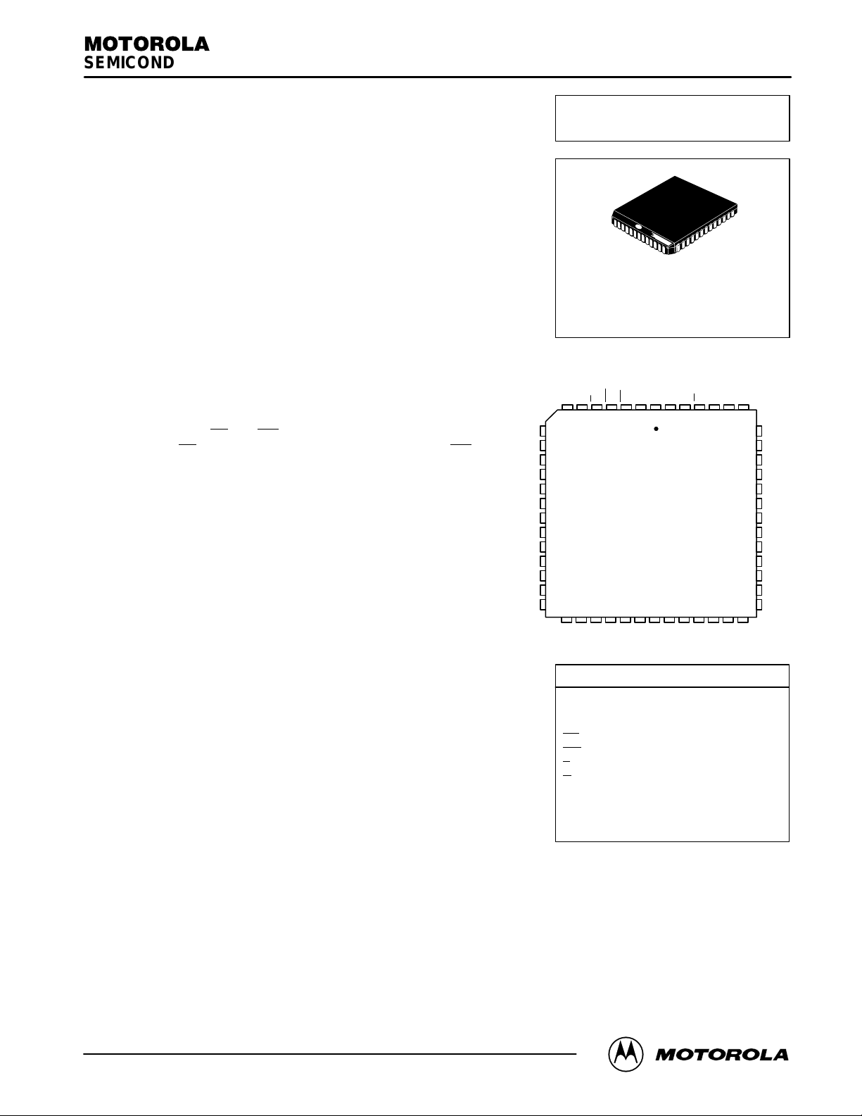
The MCM67A618B will be available in a 52–pin plastic leaded chip
carrier (PLCC).
This device is ideally suited for systems that require wide data bus
widths, cache memory , and tag RAMs.
• Single 5 V
± 5% Power Supply
• Fast Access Times: 10/12/15 ns Max
• Byte Writeable via Dual Write Enables
• Separate Data Input Latch for Simplified Write Cycles
• Address and Chip Enable Input Latches
• Common Data Inputs and Data Outputs
• Output Enable Controlled Three–State Outputs
• 3.3 V I/O Compatible
• High Board Density 52–Lead PLCC Package
DQ9
DQ10
V
CC
V
DQ11
DQ12
DQ13
DQ14
V
V
CC
DQ15
DQ16
DQ17
MCM67A618B
FN PACKAGE
PIN ASSIGNMENT
A6A7E
8
9
10
11
SS
12
13
14
15
16
SS
17
18
19
20
A4A3A2
A5
A0 – A15 Address Inputs. . . . . . . . . . . . . . . .
AL Address Latch. . . . . . . . . . . . . . . . . . . . . .
DL Data Latch. . . . . . . . . . . . . . . . . . . . . . . . .
LW
UW
E
G
DQ0 – DQ17 Data Input/Output. . . . . . . . . . .
V
CC
V
SS
LW
UW
A1
PIN NAMES
Order this document
by MCM67A618B/D
PLASTIC
CASE 778–02
SS
CC
AL
DL
V
V
A0
SS
CC
A15
V
V
Lower Byte Write Enable. . . . . . . . . . . .
Higher Byte Write Enable. . . . . . . . . . . .
+ 5 V Power Supply. . . . . . . . . . . . . . . .
G
A8A9A10
A13
A14
Chip Enable. . . . . . . . . . . . . . . . . . . . . . . . .
Output Enable. . . . . . . . . . . . . . . . . . . . . .
4748495051521234567
33323130292827262524232221
A12
46
45
44
43
42
41
40
39
38
37
36
35
34
Ground. . . . . . . . . . . . . . . . . . . . . . . . . . .
DQ8
DQ7
DQ6
V
CC
V
SS
DQ5
DQ4
DQ3
DQ2
V
SS
V
CC
DQ1
DQ0
A11
All power supply and ground pins must be connected for proper operation of the device.
This document contains information on a new product. Specifications and information herein are subject to change without notice.
REV 2
7/16/97
Motorola, Inc. 1997
MOTOROLA FAST SRAM
MCM67A618B
1
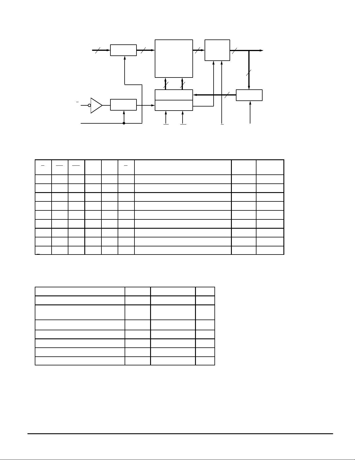
BLOCK DIAGRAM
E
AL
A0 – A15
16
LATCH
LATCH
16
MEMORY ARRAY
64K x 18
9 9
WRITE AMP
CONTROL
LW
UW G
18
OUTPUT
BUFFER
18
18
DQ0 – DQ17
18
LATCH
DL
TRUTH TABLE
Supply
E LW UW AL* DL* G Mode
H X X X X X Deselected Cycle I
L X X L X X Read or Write Using Latched Addresses I
L X X H X X Read or Write Using Unlatched Addresses I
L H H X X L Read Cycle I
L H H X X H Read Cycle I
L L L X L X Write Both Bytes Using Latched Data In I
L L L X H X Write Both Bytes Using Unlatched Data In I
L L H X X X Write Cycle, Lower Byte I
L H L X X X Write Cycle, Lower Byte I
*E and Addresses satisfy the specified setup and hold times for the falling edge of AL. Data–in satisfies the specified setup
*and hold times for falling edge of DL.
NOTE: This truth table shows the application of each function. Combinations of these functions are valid.
Current
SB
CC
CC
CC
CC
CC
CC
CC
CC
I/O
Status
High–Z
—
—
Data Out
High–Z
High–Z
High–Z
High–Z
High–Z
ABSOLUTE MAXIMUM RATINGS (Voltages Referenced to V
Rating
Power Supply Voltage V
Voltage Relative to VSS for Any
Pin Except V
Output Current (per I/O) I
Power Dissipation P
Temperature Under Bias T
Ambient Temperature T
Storage Temperature T
NOTE: Permanent device damage may occur if ABSOLUTE MAXIMUM RATINGS are
CC
exceeded. Functional operation should be restricted to RECOMMENDED OPERATING CONDITIONS. Exposure to higher than recommended voltages for
extended periods of time could affect device reliability.
Symbol Value Unit
CC
Vin, V
out
bias
stg
– 0.5 to VCC + 0.5 V
out
D
A
– 55 to + 125 °C
= 0)
SS
– 0.5 to 7.0 V
± 30
1.6 W
– 10 to + 85 °C
0 to + 70 °C
mA
MCM67A618B
2
This device contains circuitry to protect the
inputs against damage due to high static
voltages or electric fields; however, it is advised
that normal precautions be taken to avoid
application of any voltage higher than maximum rated voltages to this high–impedance
circuit.
This BiCMOS memory circuit has been
designed to meet the dc and ac specifications
shown in the tables, after thermal equilibrium
has been established.
This device contains circuitry that will ensure
the output devices are in High–Z at power up.
MOTOROLA FAST SRAM
DC OPERA TING CONDITIONS AND CHARACTERISTICS
(VCC = 5.0 V ± 5%, TA = 0 to + 70°C, Unless Otherwise Noted)
RECOMMENDED OPERATING CONDITIONS
Parameter
Supply Voltage (Operating Voltage Range) V
Input High Voltage V
Input Low Voltage V
*VIL (min) = – 0.5 V dc; VIL (min) = – 2.0 V ac (pulse width ≤ 20 ns) for I ≤ 20.0 mA.
**VIH (max) = VCC + 0.3 V dc; VIH (max) = VCC + 2.0 V ac (pulse width ≤ 20 ns) for I ≤ 20.0 mA.
(Voltages referenced to VSS = 0 V)
Symbol Min Max Unit
DC CHARACTERISTICS
Parameter Symbol Min Max Unit
Input Leakage Current (All Inputs, Vin = 0 to VCC) I
Output Leakage Current (G = VIH) I
AC Supply Current (Device Selected, All Outputs Open, MCM67A618B–10
Freq = Max, VCC = Max) MCM67A618B–12
MCM67A618B–15
CMOS Standby Supply Current (Device Deselected,
Freq = 0, VDD = Max, All Inputs Static at CMOS Levels
Vin ≤ VSS + 0.2 V or ≥ VCC – 0.2 V)
AC Standby Supply Current (Device Deselected, MCM67A618B–10
Freq = Max, VDD = Max, All Inputs Toggling at CMOS Levels
Vin ≤ VSS + 0.2 V or ≥ VCC – 0.2 V)
Output Low Voltage (IOL = + 8.0 mA) V
Output High Voltage (IOH = – 4.0 mA) V
lkg(I)
lkg(O)
I
CCA
I
SB2
I
SB4
CC
IH
IL
OL
OH
4.75 5.25 V
2.2
– 0.5*
— ± 1.0 µA
— ± 1.0 µA
— TBD mA
— TBD mA
— TBD mA
— 0.4 V
2.4 3.3 V
VCC + 0.3**
0.8 V
V
CAPACITANCE (f = 1.0 MHz, dV = 3.0 V, T
Characteristic
Input Capacitance C
Input/Output Capacitance C
= 25°C, Periodically Sampled Rather Than 100% Tested)
A
Symbol Typ Max Unit
in
I/O
4 5 pF
6 8 pF
MOTOROLA FAST SRAM
MCM67A618B
3
AC OPERA TING CONDITIONS AND CHARACTERISTICS
(VCC = 5.0 V ± 5%, TA = 0 to + 70°C, Unless Otherwise Noted)
Input Timing Measurement Reference Level 1.5 V. . . . . . . . . . . . . . .
Input Pulse Levels 0 to 3.0 V. . . . . . . . . . . . . . . . . . . . . . . . . . . . . . . . .
Input Rise/Fall Time 3 ns. . . . . . . . . . . . . . . . . . . . . . . . . . . . . . . . . . . .
ASYNCHRONOUS READ CYCLE TIMING (See Notes 1 and 2)
MCM67A618B–10 MCM67A618B–12 MCM67A618B–15
Parameter Symbol Min Max Min Max Min Max Unit Notes
Read Cycle Times t
Access Times:
Output Hold from Address Change t
Output Buffer Control:
Power Up Time t
NOTES:
1. AL and DL are equal to VIH for all asynchronous cycles.
2. Both Write Enable signals (L W
3. All read cycle timing is referenced from the last valid address to the first transitioning address.
4. Addresses valid prior to or coincident with E
5. Transition is measured ± 500 mV from steady–state voltage. This parameter is sampled and not 100% tested. At any given voltage and temperature, t
Address Valid to Output Valid
E
Output Enable Low to Output Valid
EHQZ
Low to Output Valid
E
Low to Output Active
G
Low to Output Active
E
High to Output High–Z
G
High to Output High–Z
is less than t
ELQX
, UW) are equal to VIH for all read cycles.
and t
GHQZ
AVAV
t
AVQV
t
ELQV
t
GLQV
AXQX
t
ELQX
t
GLQX
t
EHQZ
t
GHQZ
ELICCA
going low.
is less than t
10 — 12 — 15 — ns 3
—
—
—
4 — 4 — 4 — ns
3
1
2
2
0 — 0 — 0 — ns
GLQX
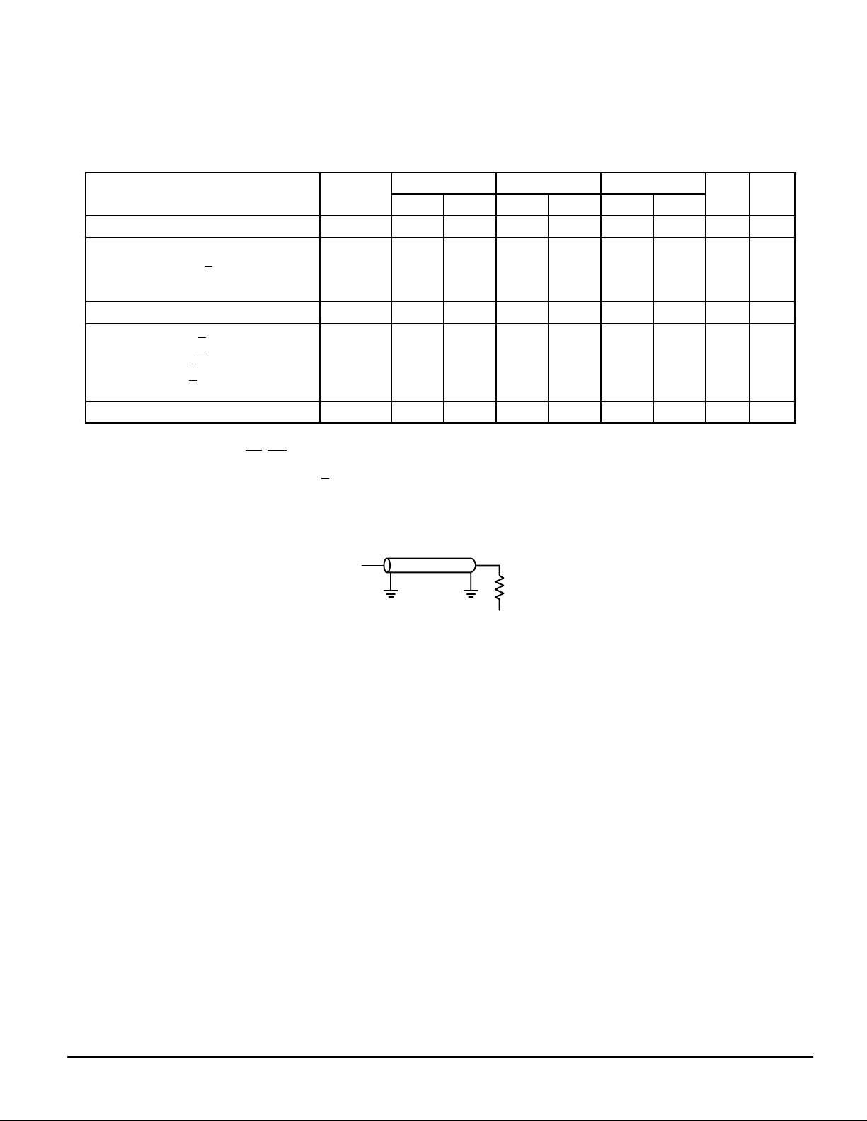
Output Timing Reference Level 1.5 V. . . . . . . . . . . . . . . . . . . . . . . . . .
Output Load Figure 1 Unless Otherwise Noted. . . . . . . . . . . . . . . . . .
10
10
5
—
—
5
5
for a given device.
—
—
—
3
1
2
2
12
12
—
—
—
6
6
6
—
—
3
1
2
2
15
15
7
—
—
7
7
ns 4
ns 5
OUTPUT
Z0 = 50
Ω
VL = 1.5 V
Figure 1. AC Test Load
RL = 50
Ω
MCM67A618B
4
MOTOROLA FAST SRAM
 Loading...