

Motorola MCM6706CRJ5.5, MCM6706CRJ5.5R, MCM6706CRJ5, MCM6706CRJ5R Datasheet
MOTOROLA
SEMICONDUCTOR TECHNICAL DATA
Product Preview
32K x 8 Bit Static Random
Order this document
by MCM6706CR/D
MCM6706CR
Access Memory
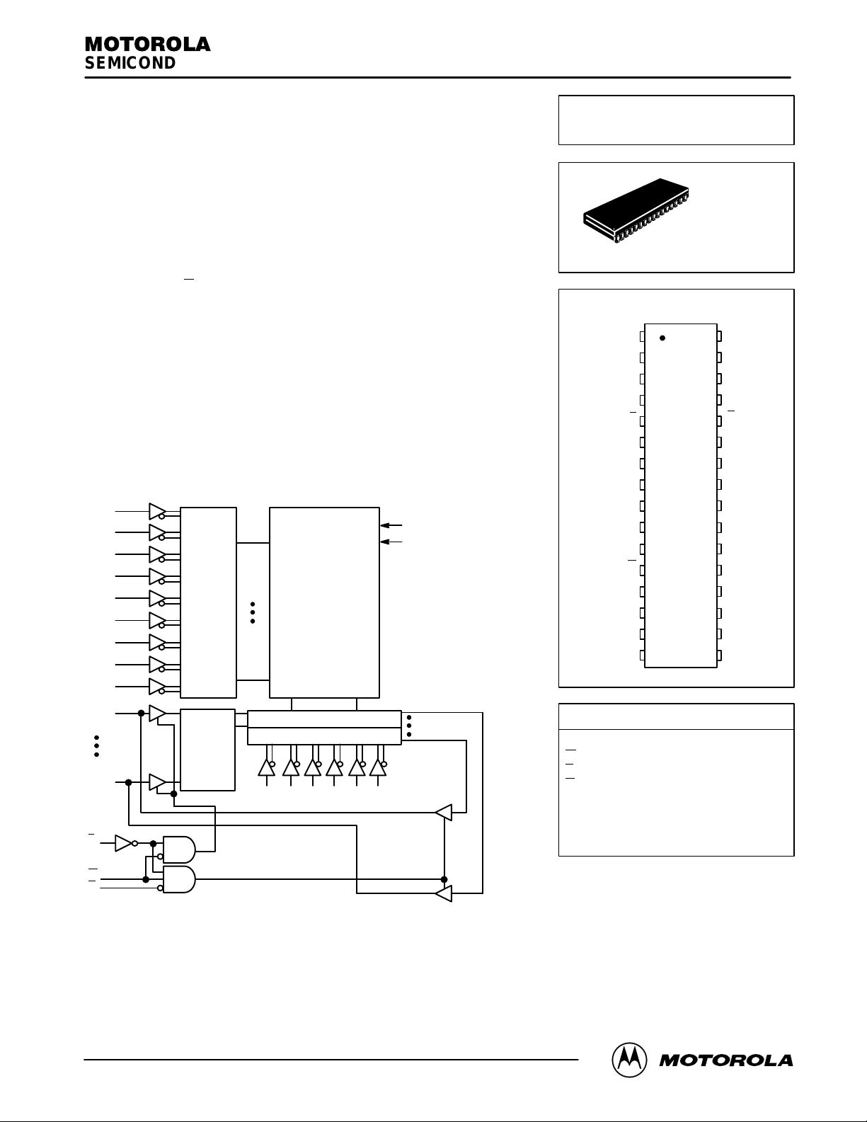
The MCM6706CR is a 262,144 bit static random access memory organized
as 32,768 words of 8 bits. Static design eliminates the need for external clocks
or timing strobes.
Output enable (G
flexibility and eliminates bus contention problems.
The MCM6706CR meets JEDEC standards and is available in a revolutionary
pinout 300 mil, 32–lead surface–mount SOJ package.
• Single 5.0 V ± 10% Power Supply
• Fully Static — No Clock or Timing Strobes Necessary
• All Inputs and Outputs Are TTL Compatible
• Three State Outputs
• Fast Access Times: MCM6706CR–5 = 5 ns
• Center Power and I/O Pins for Reduced Noise
A
A
A
A
A
A
A
A
A
) is a special control feature that provides increased system
MCM6706CR–5.5 = 5.5 ns
BLOCK DIAGRAM
V
CC
V
SS
ROW
DECODER
MEMORY
MATRIX
512 ROWS x 64 x 8
COLUMNS
J PACKAGE
300 MIL SOJ
CASE 857–02
PIN ASSIGNMENT
ANC
V
V
DQ
DQ
CC
SS
DQ
DQ
W
1
A
2
A
3
A
4
E
5
6
7
8
9
10
11
12
A
13
A
14
A
15
A
16
32
31
30
29
28
27
26
25
24
23
22
21
20
19
18
17
A
A
A
G
DQ
DQ
V
V
DQ
DQ
A
A
A
A
NC
SS
CC
DQ0
INPUT
DATA
CONTROL
DQ7
E
W
G
This document contains information on a new product under development. Motorola reserves the right to change or discontinue this product without notice.
REV 1
10/9/96
Motorola, Inc. 1996
MOTOROLA FAST SRAM
COLUMN I/O
COLUMN DECODER
AA A
A A A
A Address. . . . . . . . . . . . . . . . . . . . . . . . . . . . . .
W
E
G
DQ Data Input/Output. . . . . . . . . . . . . . . . . . .
V
CC
V
SS
NC No Connection. . . . . . . . . . . . . . . . . . . . . .
PIN NAMES
Write Enable. . . . . . . . . . . . . . . . . . . . . . . . .
Chip Enable. . . . . . . . . . . . . . . . . . . . . . . . . .
Output Enable. . . . . . . . . . . . . . . . . . . . . . .
+ 5 V Power Supply. . . . . . . . . . . . . . . .
MCM6706CR
Ground. . . . . . . . . . . . . . . . . . . . . . . . . . .
1
TRUTH TABLE
E G W Mode I/O Pin Cycle
H X X Not Selected High–Z —
L H H Read High–Z —
L L H Read D
L X L Write D
out
in
Read Cycle
Write Cycle
ABSOLUTE MAXIMUM RATINGS (See Note)
Rating
Power Supply Voltage V
Voltage Relative to VSS for Any Pin
Except V
Output Current I
Power Dissipation P
Temperature Under Bias T
Operating Temperature T
Storage Temperature — Plastic T
NOTE: Permanent device damage may occur if ABSOLUTE MAXIMUM RATINGS are
CC
exceeded. Functional operation should be restricted to RECOMMENDED
OPERATING CONDITIONS. Exposure to higher than recommended voltages for
extended periods of time could affect device reliability .
Symbol Value Unit
CC
Vin, V
out
bias
stg
out
D
A
– 0.5 to + 7.0 V
– 0.5 to VCC + 0.5 V
± 30 mA
2.0 W
– 10 to + 85 °C
0 to + 70 °C
– 55 to + 125 °C
DC OPERA TING CONDITIONS AND CHARACTERISTICS
(VCC = 5.0 V ± 10%, TA = 0 to 70°C, Unless Otherwise Noted)
This device contains circuitry to protect the
inputs against damage due to high static voltages or electric fields; however, it is advised
that normal precautions be taken to avoid application of any voltage higher than maximum
rated voltages to this high–impedance circuit.
This BiCMOS memory circuit has been designed to meet the dc and ac specifications
shown in the tables, after thermal equilibrium
has been established. The circuit is in a test
socket or mounted on a printed circuit board
and transverse air flow of at least 500 linear feet
per minute is maintained.
RECOMMENDED OPERATING CONDITIONS
Parameter Symbol Min Typ Max Unit
Supply Voltage (Operating Voltage Range) V
Input High Voltage V
Input Low Voltage V
*VIH (max) = VCC + 0.3 V dc; VIH (max) = VCC + 2.0 V ac (pulse width ≤ 2.0 ns) or I ≤ 30.0 mA.
** VIL (min) = – 0.5 V dc @ 30.0 mA; VIL (min) = – 2.0 V ac (pulse width ≤ 2.0 ns) or I ≤ 30.0 mA.
CC
IH
IL
4.5 5.0 5.5 V
2.2 —
– 0.5**
— 0.8 V
VCC + 0.3*
DC CHARACTERISTICS
Parameter Symbol Min Max Unit
Input Leakage Current (All Inputs, Vin = 0 to VCC) I
Output Leakage Current (E = VIH or G = VIH, V
Output High Voltage (IOH = – 4.0 mA) V
Output Low Voltage (IOL = + 8.0 mA) V
= 0 to VCC) I
out
lkg(I)
lkg(O)
OH
OL
— ± 1.0 µA
— ± 1.0 µA
2.4 — V
— 0.4 V
POWER SUPPLY CURRENTS
Parameter Symbol MCM6706CR–5 MCM6706CR–5.5 Unit Notes
AC Active Supply Current
(I
= 0 mA, VCC = max, f = f
out
AC Standby Current (E = VIH, VCC = max, f = f
CMOS Standby Current (VCC = max, f = 0 MHz,
E
≥ VCC – 0.2 V, Vin ≤ VSS, or ≥ VCC – 0.2 V)
NOTES:
1. Reference AC Operating Conditions and Characteristics for input and timing (VIH/VIL, tr/tf, pulse level 0 to 3.0 V, VIH = 3.0 V).
2. All addresses transition simultaneously low (LSB) and then high (MSB).
3. Data states are all zero.
max
)
) I
max
I
CCA
SB1
I
SB2
240 235 mA 1, 2, 3
120 115 mA 1, 2, 3
30 30 mA
V
MCM6706CR
2
MOTOROLA FAST SRAM
CAPACITANCE (f = 1.0 MHz, dV = 3.0 V, T
Address Input Capacitance C
Control Pin Input Capacitance (E, G, W) C
I/O Capacitance C
= 25°C, Periodically Sampled Rather Than 100% Tested)
A
Parameter
Symbol Max Unit
in
in
out
5 pF
6 pF
6 pF
AC OPERA TING CONDITIONS AND CHARACTERISTICS
(VCC = 5.0 V ± 10%, TA = 0 to + 70°C, Unless Otherwise Noted)
Input Timing Measurement Reference Level 1.5 V. . . . . . . . . . . . . . .
Input Pulse Levels 0 to 3.0 V. . . . . . . . . . . . . . . . . . . . . . . . . . . . . . . . .
Input Rise/Fall Time 2 ns. . . . . . . . . . . . . . . . . . . . . . . . . . . . . . . . . . . .
READ CYCLE (See Notes 1 and 2)
Parameter Symbol Min Max Min Max Unit Notes
Read Cycle Time t
Address Access Time t
Chip Enable Access Time t
Output Enable Access Time t
Output Hold from Address Change t
Chip Enable Low to Output Active t
Chip Enable High to Output High–Z t
Output Enable Low to Output Active t
Output Enable High to Output High–Z t
NOTES:
1. W
is high for read cycle.
2. Product sensitivities to noise require proper grounding and decoupling of power supplies as well as minimization or elimination of bus
contention conditions during read and write cycles.
3. All read cycle timing is referenced from the last valid address to the first transitioning address.
4. At any given voltage and temperature, t
device to device.
5. Transition is measured 200 mV from steady–state voltage with load of Figure 1b.
6. This parameter is sampled and not 100% tested.
7. Device is continuously selected (E
8. Addresses valid prior to or coincident with E
= VIL, G = VIL).
AVAV
AVQV
ELQV
GLQV
AXQX
ELQX
EHQZ
GLQX
GHQZ
EHQZ
going low.
max < t
ELQX
Output Timing Measurement Reference Level 1.5 V. . . . . . . . . . . . .
Output Load See Figure 1a. . . . . . . . . . . . . . . . . . . . . . . . . . . . . . . . . .
MCM6706CR–5 MCM6706CR–5.5
5 — 5.5 — ns 3
— 5 — 5.5 ns
— 5 — 5.5 ns
— 4 — 4 ns
2.0 — 2.0 — ns
3 — 3 — ns 4 ,5, 6
— 3 — 3 ns 4, 5, 6
0 — 0 — ns 4, 5, 6
— 3 — 3 ns 4, 5, 6
min, and t
GHQZ
max < t
min, both for a given device and from
GLQX
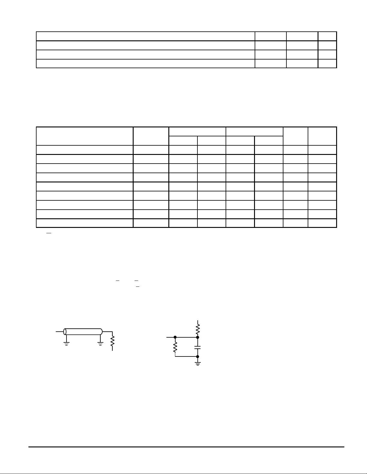
OUTPUT
Z0 = 50
Ω
(a) (b)
MOTOROLA FAST SRAM
RL = 50
VL = 1.5 V
TIMING LIMITS
+5 V
480
Ω
OUTPUT
Ω
255
Ω
5 pF
The table of timing values shows either a
minimum or a maximum limit for each parameter. Input requirements are specified from
the external system point of view. Thus, address setup time is shown as a minimum
since the system must supply at least that
much time. On the other hand, responses
from the memory are specified from the device point of view. Thus, the access time is
shown as a maximum since the device never
provides data later than that time.
Figure 1. AC Test Loads
MCM6706CR
3
 Loading...