

Motorola MCM62449WJ35R2, MCM62449WJ25R2, MCM62449WJ20, MCM62449WJ20R2, MCM62449WJ25 Datasheet
...
MCM6249
1
MOTOROLA FAST SRAM
1M x 4 Bit Static Random
Access Memory
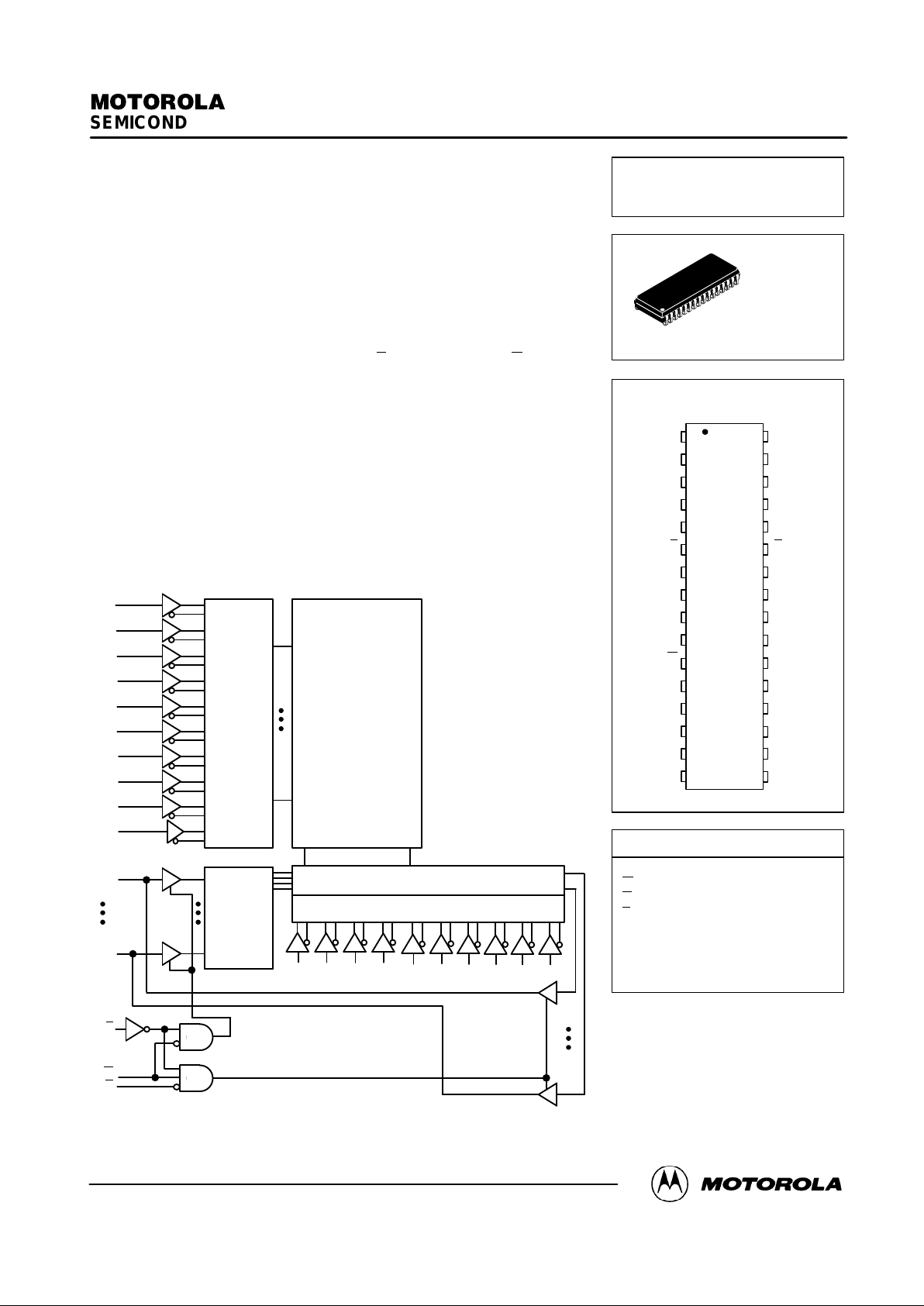
The MCM6249 is a 4,194,304 bit static random access memory organized as
1,048,576 words of 4 bits, fabricated using high–performance silicon–gate
CMOS technology. Static design eliminates the need for external clocks or timing
strobes, while CMOS circuitry reduces power consumption and provides for
greater reliability .
The MCM6249 is equipped with chip enable (E
) and output enable (G) pins,
allowing for greater system flexibility and eliminating bus contention problems.
Either input, when high, will force the outputs into high impedance.
The MCM6249 is available in a 400 mil, 32–lead surface–mount SOJ package.
• Single 5 V ± 10% Power Supply
• Fast Access Time: 20/25/35 ns
• Equal Address and Chip Enable Access Time
• All Inputs and Outputs are TTL Compatible
• Three–State Outputs
• Power Operation: 190/175/160 mA Maximum, Active AC
BLOCK DIAGRAM
G
A18 A17 A16 A15 A14 A19 A3 A2 A1 A0
MEMORY MATRIX
1024 ROWS x
4096 COLUMNS
ROW
DECODER
INPUT
DATA
CONTROL
A11
A10
A9
A8
A7
A6
A5
A4
DQ0
DQ3
E
W
A13
A12
COLUMN I/O
COLUMN DECODER
DQ0
DQ3
Order this document
by MCM6249/D
MOTOROLA
SEMICONDUCTOR TECHNICAL DATA
PIN ASSIGNMENT
MCM6249
A0 – A19 Address Inputs. . . . . . . . . . . .
W
Write Enable. . . . . . . . . . . . . . . . . . . .
G
Output Enable. . . . . . . . . . . . . . . . . . .
E
Chip Enable. . . . . . . . . . . . . . . . . . . . . .
DQ0 – DQ3 Data Input/Output. . . . . . . .
NC No Connection. . . . . . . . . . . . . . . . .
V
CC
+ 5 V Power Supply. . . . . . . . . . . .
V
SS
Ground. . . . . . . . . . . . . . . . . . . . . . .
PIN NAMES
WJ PACKAGE
400 MIL SOJ
CASE 857A–02
32
31
30
29
28
27
26
25
24
23
22
21
2
3
1
5
6
4
7
9
10
8
12
13
11
14
20
15
16
19
18
17
A8
A9
A17
A6
E
A11
W
A13
A18
A10
V
CC
A16
A14
A3
A15
DQ2
A2
G
DQ3
A4
A19
A5
A0
V
SS
V
CC
V
SS
DQ0
DQ1
A7
A1
A12 NC
REV 4
5/95
Motorola, Inc. 1995
MCM6249
2
MOTOROLA FAST SRAM
TRUTH TABLE (X = Don’t Care)
E
G W Mode I/O Pin Cycle Current
H X X Not Selected High–Z — I
SB1
, I
SB2
L H H Output Disabled High–Z — I
CCA
L L H Read D
out
Read I
CCA
L X L Write High–Z Write I
CCA
ABSOLUTE MAXIMUM RATINGS (See Note)
Rating
Symbol Value Unit
Power Supply Voltage Relative to V
SS
V
CC
– 0.5 to + 7.0 V
Voltage Relative to VSS for Any Pin
Except V
CC
Vin, V
out
– 0.5 to VCC + 0.5 V
Output Current (per I/O) I
out
± 20
mA
Power Dissipation P
D
1.0 W
Temperature Under Bias T
bias
– 10 to + 85 °C
Operating Temperature T
A
0 to + 70 °C
Storage Temperature — Plastic T
stg
– 55 to + 150 °C
NOTE: Permanent device damage may occur if ABSOLUTE MAXIMUM RATINGS are
exceeded. Functional operation should be restricted to RECOMMENDED OPERATING CONDITIONS. Exposure to higher than recommended voltages for
extended periods of time could affect device reliability.
DC OPERA TING CONDITIONS AND CHARACTERISTICS
(VCC = 5.0 V ± 10%, TA = 0 to + 70°C, Unless Otherwise Noted)
RECOMMENDED OPERATING CONDITIONS
Parameter Symbol Min Typ Max Unit
Supply Voltage (Operating Voltage Range) V
CC
4.5 5.0 5.5 V
Input High Voltage V
IH
2.2 — VCC + 0.3 V
Input Low Voltage V
IL
– 0.5*
— 0.8 V
*VIL (min) = – 0.5 V dc; VIL (min) = – 2.0 V ac (pulse width ≤ 2.0 ns).
DC CHARACTERISTICS
Parameter Symbol Min Max Unit
Input Leakage Current (All Inputs, Vin = 0 to VCC) I
lkg(I)
— ± 1.0 µA
Output Leakage Current (E = VIH, V
out
= 0 to VCC) I
lkg(O)
— ± 1.0 µA
Output Low Voltage (IOL = + 8.0 mA) V
OL
— 0.4 V
Output High Voltage (IOH = – 4.0 mA) V
OH
2.4 — V
POWER SUPPLY CURRENTS
Parameter Symbol Min Typ Max Unit
AC Active Supply Current (I
out
= 0 mA, MCM6249–20: t
AVAV
= 20 ns
VCC = max) MCM6249–25: t
AVAV
= 25 ns
MCM6249–35: t
AVAV
= 35 ns
I
CC
—
—
—
175
160
145
190
175
160
mA
AC Standby Current (VCC = max, MCM6249–20: t
AVAV
= 20 ns
E
= VIH, No other restrictions on MCM6249–25: t
AVAV
= 25 ns
other inputs) MCM6249–35: t
AVAV
= 35 ns
I
SB1
—
—
—
50
40
35
60
50
40
mA
CMOS Standby Current (E ≥ VCC – 0.2 V , Vin ≤ VSS + 0.2 V or
≥ VCC – 0.2 V) (VCC = max, f = 0 MHz)
I
SB2
— 10 15 mA
This device contains circuitry to protect the
inputs against damage due to high static
voltages or electric fields; however, it is advised that normal precautions be taken to avoid
application of any voltage higher than maximum rated voltages to these high impedance
circuits.
This CMOS memory circuit has been designed to meet the dc and ac specifications
shown in the tables, after thermal equilibrium
has been established. The circuit is in a test
socket or mounted on a printed circuit board
and transverse air flow of at least 500 linear
feet per minute is maintained.
MCM6249
3
MOTOROLA FAST SRAM
CAPACITANCE (f = 1.0 MHz, dV = 3.0 V, T
A
= 25°C, Periodically Sampled Rather Than 100% Tested)
Parameter
Symbol Typ Max Unit
Input Capacitance All Inputs Except Clocks and DQs
E
, G, W
C
in
C
ck
4
5
6
8
pF
Input/Output Capacitance DQ C
I/O
5 8 pF
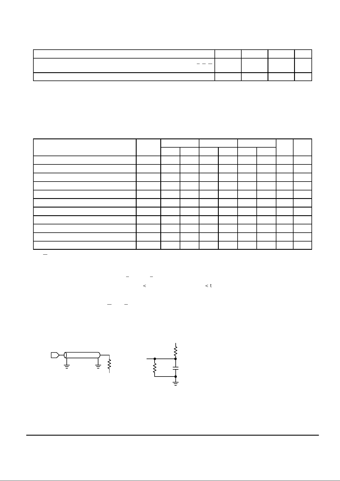
AC OPERA TING CONDITIONS AND CHARACTERISTICS
(VCC = 5.0 V ± 10%, TA = 0 to + 70°C, Unless Otherwise Noted)
Input Pulse Levels 0 to 3.0 V. . . . . . . . . . . . . . . . . . . . . . . . . . . . . . . . .
Input Rise/Fall Time 2 ns. . . . . . . . . . . . . . . . . . . . . . . . . . . . . . . . . . . .
Input Timing Measurement Reference Level 1.5 V. . . . . . . . . . . . . . .
Output Timing Measurement Reference Level 1.5 V. . . . . . . . . . . . .
Output Load See Figure 1a. . . . . . . . . . . . . . . . . . . . . . . . . . . . . . . . . .
READ CYCLE TIMING (See Note 1)
MCM6249–20 MCM6249–25 MCM6249–35
Parameter Symbol Min Max Min Max Min Max Unit Notes
Read Cycle Time t
AVAV
20 — 25 — 35 — ns 2, 3
Address Access Time t
AVQV
— 20 — 25 — 35 ns
Enable Access Time t
ELQV
— 20 — 25 — 35 ns 4
Output Enable Access Time t
GLQV
— 6 — 8 — 10 ns
Output Hold from Address Change t
AXQX
5 — 5 — 5 — ns
Enable Low to Output Active t
ELQX
5 — 5 — 5 — ns 5, 6, 7
Output Enable Low to Output Active t
GLQX
0 — 0 — 0 — ns 5, 6, 7
Enable High to Output High–Z t
EHQZ
0 9 0 10 0 12 ns 5, 6, 7
Output Enable High to Output High–Z t
GHQZ
0 9 0 10 0 12 ns 5, 6, 7
Power Up Time t
ELICCH
0 — 0 — 0 — ns
Power Down Time t
EHICCL
— 20 — 25 — 35 ns
NOTES:
1. W
is high for read cycle.
2. Product sensitivities to noise require proper grounding and decoupling of power supplies as well as minimization or elimination of bus con–
tention conditions during read and write cycles.
3. All read cycle timings are referenced from the last valid address to the first transitioning address.
4. Addresses valid prior to or coincident with E
going low/E going high.
5. At any given voltage and temperature, t
EHQZ
max t t
ELQX
min, and t
GHQZ
max t t
GLQX
min, both for a given device and from device
to device.
6. Transition is measured ± 500 mV from steady–state voltage with load of Figure 1b.
7. This parameter is sampled and not 100% tested.
8. Device is continuously selected (E
≤ VIL, G ≤ VIL).
(a) (b)
The table of timing values shows either a minimum
or a maximum limit for each parameter. Input requirements are specified from the external system
point of view. Thus, address setup time is shown as
a minimum since the system must supply at least
that much time. On the other hand, responses from
the memory are specified from the device point of
view. Thus, the access time is shown as a maximum
since the device never provides data later than that
time.
TIMING LIMITS
OUTPUT
Z0 = 50
Ω
RL = 50
Ω
VL = 1.5 V
5 pF
+ 5 V
OUTPUT
255
Ω
480
Ω
Figure 1. AC Test Loads
 Loading...