

Motorola MCM62110FN20, MCM62110FN15, MCM62110FN17 Datasheet
MCM62110
1
MOTOROLA FAST SRAM
32K x 9 Bit Synchronous Dual I/O
or Separate I/O Fast Static RAM
with Parity Checker
The MCM62110 is a 294,912 bit synchronous static random access memory
organized as 32,768 words of 9 bits, fabricated using Motorola’s high–performance silicon–gate CMOS technology. The device integrates a 32K x 9 SRAM
core with advanced peripheral circuitry consisting of address registers, two sets
of input data registers, two sets of output latches, active high and active low chip
enables, and a parity checker. The RAM checks odd parity during RAM read
cycles. The data parity error (DPE
) output is an open drain type output which indicates the result of this check. This device has increased output drive capability
supported by multiple power pins. In addition, the output levels can be either 3.3 V
or 5 V TTL compatible by choice of the appropriate output bus power supply.
The device has both asynchronous and synchronous inputs. Asynchronous
inputs include the p rocessor o utput enable (POE
), system o utput enable (SOE), a nd
the clock (K).
The address (A0 – A14) and chip enable (E1
and E2) inputs are synchronous
and are registered on the falling edge of K. Write enable (W
), processor input
enable (PIE
) and system input enable (SIE) are registered on the rising edge
of K. Writes to the RAM are self–timed.
All data inputs/outputs, PDQ0 – PDQ7, SDQ0 – SDQ7, PDQP, and SDQP
have input data registers triggered by the rising edge of the clock. These pins also
have three–state output latches which are transparent during the high level of the
clock and latched during the low level of the clock.
This device has a special feature which allows data to be passed through the
RAM between the system and processor ports in either direction. This streaming
is accomplished by latching in data from one port and asynchronously output
enabling the other port. It is also possible to write to the RAM while streaming.
Additional power supply pins have been utilized for maximum performance. The
output buffer power (V
CCQ
) and ground pins (V
SSQ
) are electrically isolated from
VSS and V
CC,
and supply power and ground only to the output buffers. This allows
connecting t he output buffers to 3 .3 V instead o f 5.0 V if desired. If 3 .3 V output l evels
are chosen, the output buffer impedance in the ‘‘high’’ state is approximately equal
to the impedance in the ‘‘low’’ state thereby allowing simplified transmission line terminations.
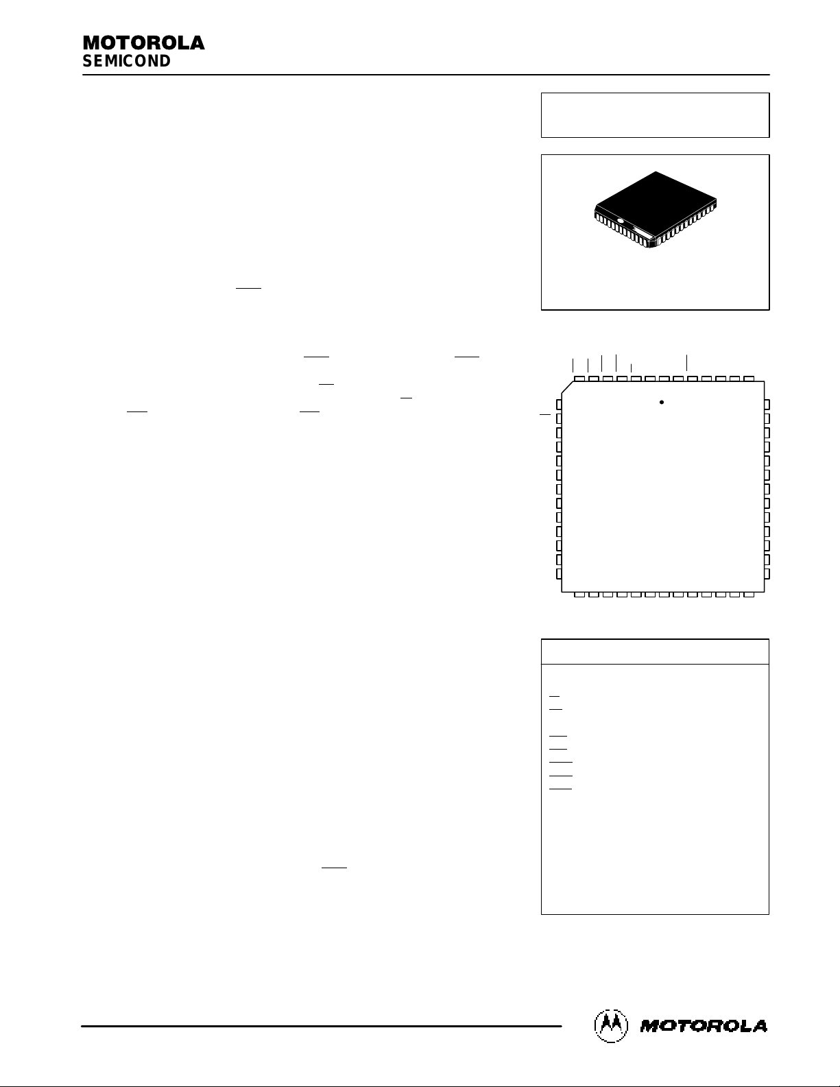
The MCM62110 is available in a 52–pin plastic leaded chip carrier (PLCC).
This device is ideally suited for pipelined systems and systems with multiple
data buses and multiprocessing systems, where a local processor has a bus isolated from a common system bus.
• Single 5 V ± 10% Power Supply
• Choice of 5 V or 3.3 V ± 10% Power Supplies for Output Level
Compatibility
• Fast Access and Cycle Times: 15/17/20 ns Max
• Self–Timed Write Cycles
• Clock Controlled Output Latches
• Address, Chip Enable, and Data Input Registers
• Common Data Inputs and Data Outputs
• Dual I/O for Separate Processor and Memory Buses
• Separate Output Enable Controlled Three–State Outputs
• Odd Parity Checker During Reads
• Open Drain Output on Data Parity Error (DPE
) Allowing Wire–ORing of
Outputs
• High Output Drive Capability: 85 pF/Output at Rated Access Time
• High Board Density 52 Lead PLCC Package
• Active High and Low Chip Enables for Easy Memory Depth Expansion
• Can be used as Separate I/O x9
PIN ASSIGNMENT
10
9
8
12
11
15
14
13
17
16
20
19
18
37
38
34
35
36
42
43
39
40
41
45
46
44
21 22 23 24 25 26 2728 29 30 31 3233
7 6 5 4 3 2 1 52 51 50 49 4847
E2
E1
PDQ7
SDQ7
V
SSQ
PDQ5
V
CCQ
PDQ3
SDQ3
V
SSQ
PDQ1
SDQ1
SDQ5
PDQP
SDQP
V
SSQ
PDQ6
SDQ6
V
CCQ
PDQ4
SDQ4
PDQ2
SDQ2
V
SSQ
PDQ0
SDQ0
SIE
PIE
SOE
POEWK
VCCVSSDPEA6A4
A2
V
SS
V
CC
A14
A13
A12
A11
A10
A9A8A7A5A3
A1 A0
All power supply and ground pins must be
connected for proper operation of the device.
VCC ≥ V
CCQ
at all times including power up.
PIN NAMES
A0 – A14 Address Inputs. . . . . . . . . . . . . . .
K Clock Input. . . . . . . . . . . . . . . . . . . . . . . . .
W
Write Enable. . . . . . . . . . . . . . . . . . . . . . .
E1
Active Low Chip Enable. . . . . . . . . . . . .
E2 Active High Chip Enable. . . . . . . . . . . . .
PIE
Processor Input Enable. . . . . . . . . . . . .
SIE
System Input Enable. . . . . . . . . . . . . . .
POE Processor Output Enable. . . . . . . . . .
SOE
System Output Enable. . . . . . . . . . . . .
DPE
Data Parity Error. . . . . . . . . . . . . . . . . .
PDQ0 – PDQ7 Processor Data I/O. . . . . . .
PDQP Processor Data Parity. . . . . . . . . . .
SDQ0 – SDQ7 System Data I/O. . . . . . . . .
SDQP System Data Parity. . . . . . . . . . . . .
V
CC
+ 5 V Power Supply. . . . . . . . . . . . . . .
V
CCQ
Output Buffer Power Supply. . . . . .
V
SSQ
Output Buffer Ground. . . . . . . . . . . .
V
SS
Ground. . . . . . . . . . . . . . . . . . . . . . . . . .
Order this document
by MCM62110/D
MOTOROLA
SEMICONDUCTOR TECHNICAL DATA
MCM62110
FN PACKAGE
PLASTIC
CASE 778–02
REV 3
5/95
Motorola, Inc. 1994
MCM62110
2
MOTOROLA FAST SRAM
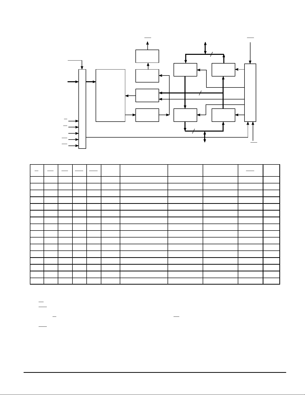
BLOCK DIAGRAM
K
9
9
9
REGISTER
CONTROL
WRITE
DRIVER
A0 – A14
W
E1
E2
PIE
SIE
DPE POE
SOE
32K × 9 ARRAY
DATA
REGISTER
DATA
REGISTER
DATA
REGISTER
DATA
LATCH
DATA
LATCH
SENSE
AMPLIFIER
PARITY
CHECK
SDQ0 – SDQ7, SDQP
PDQ0 – PDQ7, PDQP
FUNCTIONAL TRUTH TABLE (See Notes 1 and 2)
W
PIE SIE POE SOE Mode
Memory Subsystem
Cycle
PDQ0 – PDQ7,
PDQP Output
SDQ0 – SDQ7,
SDQP Output
DPE Notes
1 1 1 0 1 Read Processor Read Data Out High–Z Parity Out 3, 4
1 1 1 1 0 Read Copy Back High–Z Data Out Parity Out 3, 4
1 1 1 0 0 Read Dual Bus Read Data Out Data Out Parity Out 3, 4
1 X X 1 1 Read NOP High–Z High–Z 1
X 0 0 X X N/A NOP High–Z High–Z 1 2, 5
0 0 1 1 1 Write Processor Write Hit Data In High–Z 1 2, 6
0 1 0 1 1 Write Allocate High–Z Data In 1 2
0 0 1 1 0 Write Write Through Data In Stream Data 1 2, 7
0 1 0 0 1 Write Allocate With Stream Stream Data Data In 1 2, 7
1 0 1 1 0 N/A Cache Inhibit Write Data In Stream Data 1 2, 7
1 1 0 0 1 N/A Cache Inhibit Read Stream Data Data In 1 2, 7
0 1 1 X X N/A NOP High–Z High–Z 1 5
X 0 1 0 0 N/A Invalid Data In Stream 1 2, 8
X 0 1 0 1 N/A Invalid Data In High–Z 1 2, 8
X 1 0 0 0 N/A Invalid Stream Data In 1 2, 8
X 1 0 1 0 N/A Invalid High–Z Data In 1 2, 8
NOTES:
1. A ‘0’ represents an input voltage ≤ VIL and a ‘1’ represents an input voltage ≥ VIH. All inputs must satisfy the specified setup and hold times
for the falling or rising edge of K. Some entries in this truth table represent latched values. This table assumes that the chip is selected (i.e.,
E1
= 0 and E2 = 1) and VCC current is equal to I
CCA
. If this is not true, the chip will be in standby mode, the VCC current will equal I
SB1
or I
SB2
DPE
will default to 1 and all RAM outputs will be in High–Z. Other possible combinations of control inputs not covered by this note or the table
above are not supported and the RAM’s behavior is not specified.
2. If either IE signal is sampled low on the rising edge of clock, the corresponding OE is a don’t care, and the corresponding outputs are High–Z.
3. A read cycle is defined as a cycle where data is driven on the internal data bus by the RAM.
4. DPE
is registered on the rising edge of K at the beginning of the following clock cycle
5. No RAM cycle is performed.
6. A write cycle is defined as a cycle where data is driven onto the internal data bus through one of the data I/O ports (PDQ0 – PDQ7 and PDQP
or SDQ0 – SDQ7 and SPDQ), and written into the RAM.
7. Data is driven on the internal data bus by one I/O port through its data input register and latched into the data output latch of the other I/O
port.
8. Data contention will occur.
MCM62110
3
MOTOROLA FAST SRAM
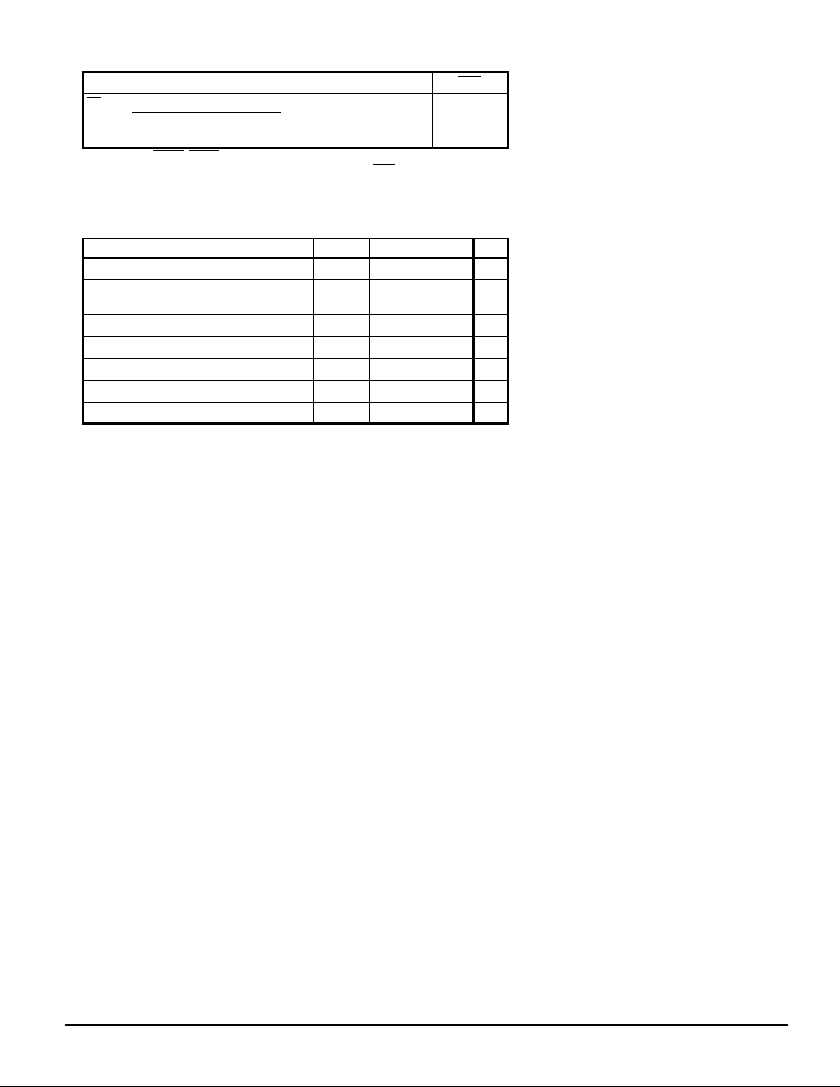
PARITY CHECKER
Parity Scheme DPE
E1 = VIH and/or E2 = V
IL
RAMP = RAM0
⊕ RAM1 ⊕ . . . ⊕ RAM7
RAMP ≠ RAM0 ⊕ RAM1 ⊕ . . . ⊕ RAM7
1
1
0
NOTE: RAMP, RAM0, RAM1 . . . , refer to the data that is present on the RAMs internal bus,
not necessarily data that resides in the RAM array. DPE
is always delayed one
clock, and is registered on the rising edge of K at the beginning of the following clock
cycle (see AC CHARACTERISTICS).
ABSOLUTE MAXIMUM RATINGS (Voltages Referenced to V
SS
= V
SSQ
= 0 V)
Rating Symbol Value Unit
Power Supply V
CC
– 0.5 to + 7.0 V
Voltage Relative to VSS/V
SSQ
for Any
Pin Except VCC and V
CCQ
Vin, V
out
– 0.5 to VCC + 0.5 V
Output Current (per I/O) I
out
± 20 mA
Power Dissipation P
D
1.2 W
Temperature Under Bias T
bias
– 10 to + 85 °C
Operating Temperature T
A
0 to +70 °C
Storage Temperature T
stg
– 55 to + 125 °C
NOTE: Permanent device damage may occur if ABSOLUTE MAXIMUM RATINGS are
exceeded. Functional operation should be restricted to RECOMMENDED OPERATING CONDITIONS. Exposure to higher than recommended voltages for
extended periods of time could affect device reliability.
ages or electric fields; however, it is advised
that normal precautions be taken to avoid
application of any voltage higher than maximum rated voltages to this high–impedance
circuit.
This CMOS memory circuit has been
designed to meet the dc and ac specifications
shown in the tables, after thermal equilibrium
has been established.
This device contains circuitry that will
ensure the output devices are in High–Z at
power up.
This device contains circuitry to protect the
inputs against damage due to high static volt
MCM62110
4
MOTOROLA FAST SRAM
DC OPERATING CONDITIONS AND CHARACTERISTICS
(VCC = 5.0 V ± 10%, V
CCQ
= 5.0 V or 3.3 V ± 10%, TA = 0 to + 70°C, Unless Otherwise Noted)
RECOMMENDED OPERATING CONDITIONS
(Voltages referenced to VSS = V
SSQ
= 0 V)
Parameter
Symbol Min Max Unit
Supply Voltage (Operating Voltage Range) V
CC
4.5 5.5 V
Output Buffer Supply Voltage (5.0 V TTL Compatible)
(3.3 V 50 Ω Compatible)
V
CCQ
4.5
3.0
5.5
3.6
V
Input High Voltage V
IH
2.2 VCC + 0.3 V
Input Low Voltage V
IL
– 0.5* 0.8 V
*VIL (min) = – 3.0 V ac (pulse width ≤ 20 ns)
DC CHARACTERISTICS
Parameter Symbol Min Max Unit
Input Leakage Current (All Inputs, Vin = 0 to VCC) I
lkg(I)
— ± 1.0 µA
Output Leakage Current (POE, SOE = VIH) I
lkg(O)
— ± 1.0 µA
AC Supply Current (All Inputs = VIL or VIH,VIL = 0.0 V and VIH ≥ 3.0 V,
I
out
= 0 mA, Cycle Time ≥ t
KHKH
min) MCM62110–15: t
KHKH
= 15 ns
MCM62110–17: t
KHKH
= 17 ns
MCM62110–20: t
KHKH
= 20 ns
I
CCA
—
—
—
190
190
190
mA
TTL Standby Current (VCC = Max, E1 = VIH or E2 = VIL) I
SB1
— 40 mA
CMOS Standby Current (VCC = Max, f = 0 MHz, E1 = VIH or E2 = VIL,
Vin ≤ VSS + 0.2 V or ≥ VCC – 0.2 V)
I
SB2
— 30 mA
Output Low Voltage (IOL = + 8.0 mA, DPE: IOL = + 23.0 mA) V
OL
— 0.4 V
Output High Voltage (IOH = – 4.0 mA) V
OH
2.4 — V
CAPACITANCE (f = 1.0 MHz, dV = 3.0 V, T
A
= 25°C, Periodically Sampled Rather Than 100% Tested)
Parameter
Symbol Typ Max Unit
Input Capacitance (All Pins Except I/Os) C
in
2 3 pF
Input/Output Capacitance (PDQ0 – PDQ7, SDQ0 – SDQ7, PDQP, SDQP) C
out
6 7 pF
Data Parity Error Output Capacitance (DPE) C
out(DPE)
6 7 pF
AC SPEC LOADS
Figure 1A Figure 1B
5 pF
+ 5 V
DQ
Figure 1C
50 pF
+ 5 V
DPE
255
Ω
480
Ω
200
Ω
DQ
Z0 = 50
Ω
RL = 50
Ω
VL = 1.5 V
 Loading...