

Motorola MCM36F8DG10, MCM36F9DG10 Datasheet
MOTOROLA
SEMICONDUCTOR TECHNICAL DATA
Advance Information
1MB and 2MB Synchronous
Order this document
by MCM36F8/D
MCM36F8
MCM36F9
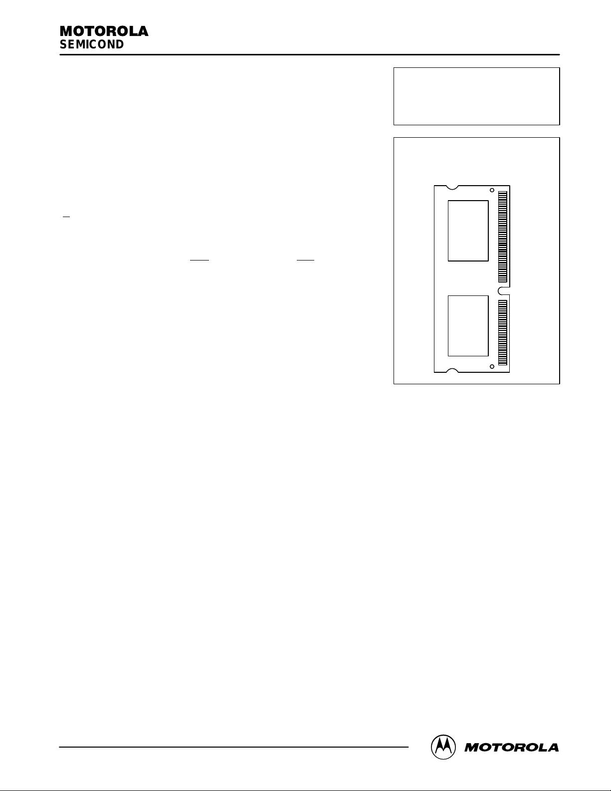
Fast Static RAM Module
The MCM36F8 (1MB) is configured as 256K x 36 bits and the MCM36F9 (2MB)
is configured as 512K x 36 bits. Both are packaged in a 144–pin dual–in–line
memory module (DIMM). Each module uses Motorola’s 3.3 V 256K x 18 bit flow–
through BurstRAMs.
Address (A), data inputs (DQ, DP), and all control signals except output enable
) are clock (K) controlled through positive–edge–triggered noninverting
(G
registers.
Write cycles are internally self–timed and initiated by the rising edge of the
clock (K) input. This feature provides increased timing flexibility for incoming
signals. Synchronous byte write (BWx
to either individual bytes or to both bytes.
• Single 3.3 V + 10%, – 5% Power Supply
• Multiple Clock Pins for Reduced Loading
• All Inputs and Outputs are L VTTL Compatible
• Byte Write and Global Write Capability
• Fast SRAM Access Times: 10 ns
• Berg Connector, Part Number: 61178–31844
• 144–Pin DIMM Module
) and global byte write (WE) allows writes
144–LEAD DIMM
CASE 1154–01
TOP VIEW
143
61
59
1
This document contains information on a new product. Specifications and information herein are subject to change without notice.
2/10/98
Motorola, Inc. 1998
MOTOROLA FAST SRAM
MCM36F8•MCM36F9
1
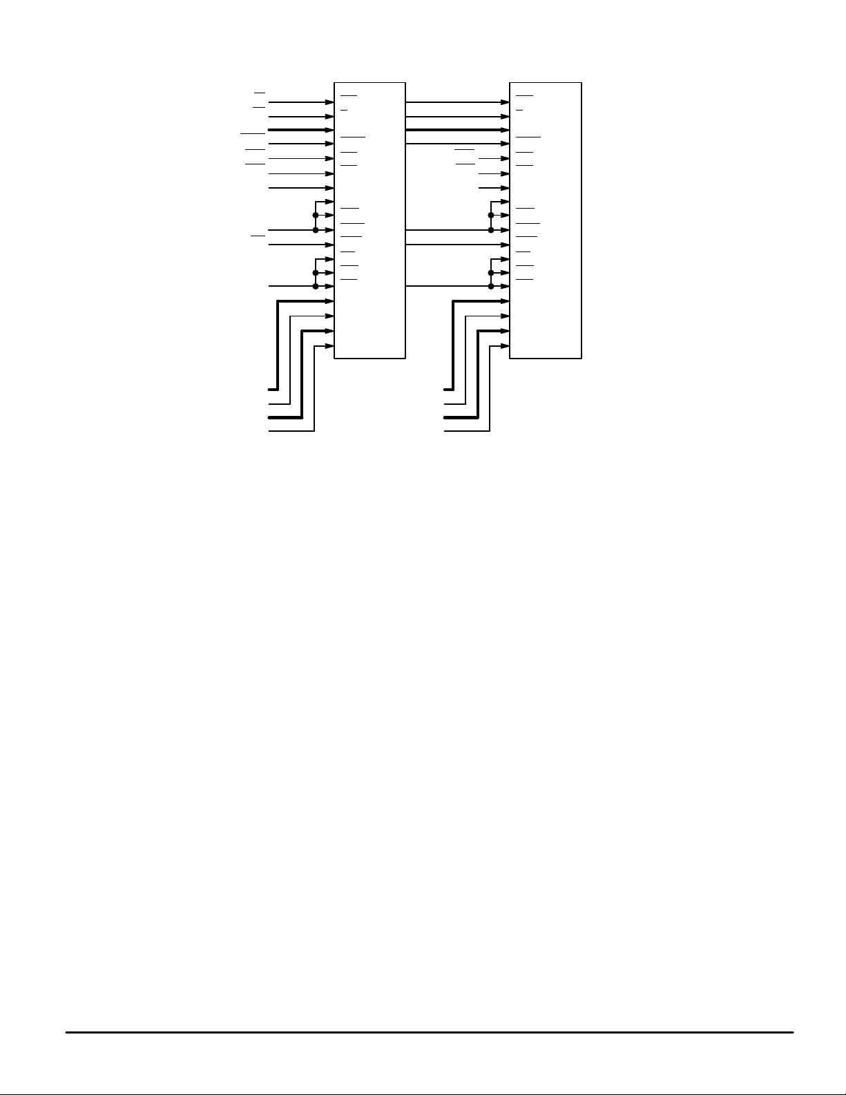
MCM36F8 BLOCK DIAGRAM
E0
G0
A0 – A17
ADSP
BW0
BW1
K0
V
DD
WE
V
SS
DQ0 – DQ7
DP0
DQ8 – DQ15
DP1
256K x 18
SE1
G
A0 – A17
ADSC
SBa
SBb
K
SE2
ADV
ADSP
SGW
SW
LBO
SE3
DQa0 – DQa7
DQa8
DQb0 – DQb7
DQb8
DQ16 – DQ23
DQ24 – DQ31
DP2
DP3
BW2
BW3
K1
256K x 18
SE1
G
A0 – A17
ADSC
SBa
SBb
K
SE2
ADV
ADSP
SGW
SW
LBO
SE3
DQa0 – DQa7
DQa8
DQb0 – DQb7
DQb8
PD1 = GND
PD0 = GND
MCM36F8•MCM36F9
2
MOTOROLA FAST SRAM
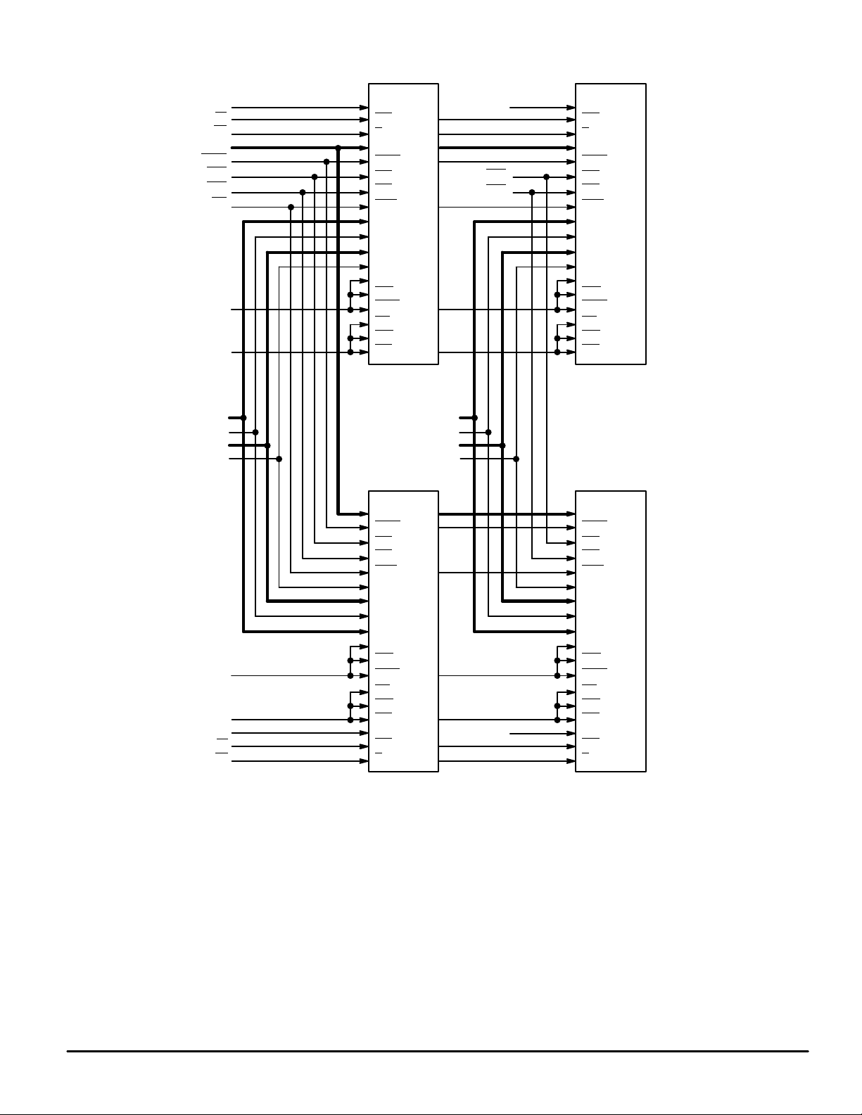
MCM36F9 BLOCK DIAGRAM
K0
E0
G0
A0 – A17
ADSP
BW0
BW1
WE
V
DD
V
SS
DQ0 – DQ7
DP0
DQ8 – DQ15
DP1
V
DD
V
SS
K2
E1
G1
256K x 18
K
SE1
G
A0 – A17
ADSC
SBa
SBb
SGW
DQa0 – DQa7
DQa8
DQb0 – DQb7
DQb8
SE2
ADV
ADSP
SW
LBO
SE3
DQ16 – DQ23
DQ24 – DQ31
256K x 18
A0 – A17
ADSC
SBa
SBb
SGW
DQb8
DQb0 – DQb7
DQa8
DQa0 – DQa7
SE2
ADV
ADSP
SW
LBO
SE3
K
SE1
G
DP2
DP3
K1
BW2
BW3
K3
256K x 18
K
SE1
G
A0 – A17
ADSC
SBa
SBb
SGW
DQa0 – DQa7
DQa8
DQb0 – DQb7
DQb8
SE2
ADV
ADSP
SW
LBO
SE3
256K x 18
A0 – A17
ADSC
SBa
SBb
SGW
DQb8
DQb0 – DQb7
DQa8
DQa0 – DQa7
SE2
ADV
ADSP
SW
LBO
SE3
K
SE1
G
PD1 = NC
PD0 = GND
MOTOROLA FAST SRAM
MCM36F8•MCM36F9
3
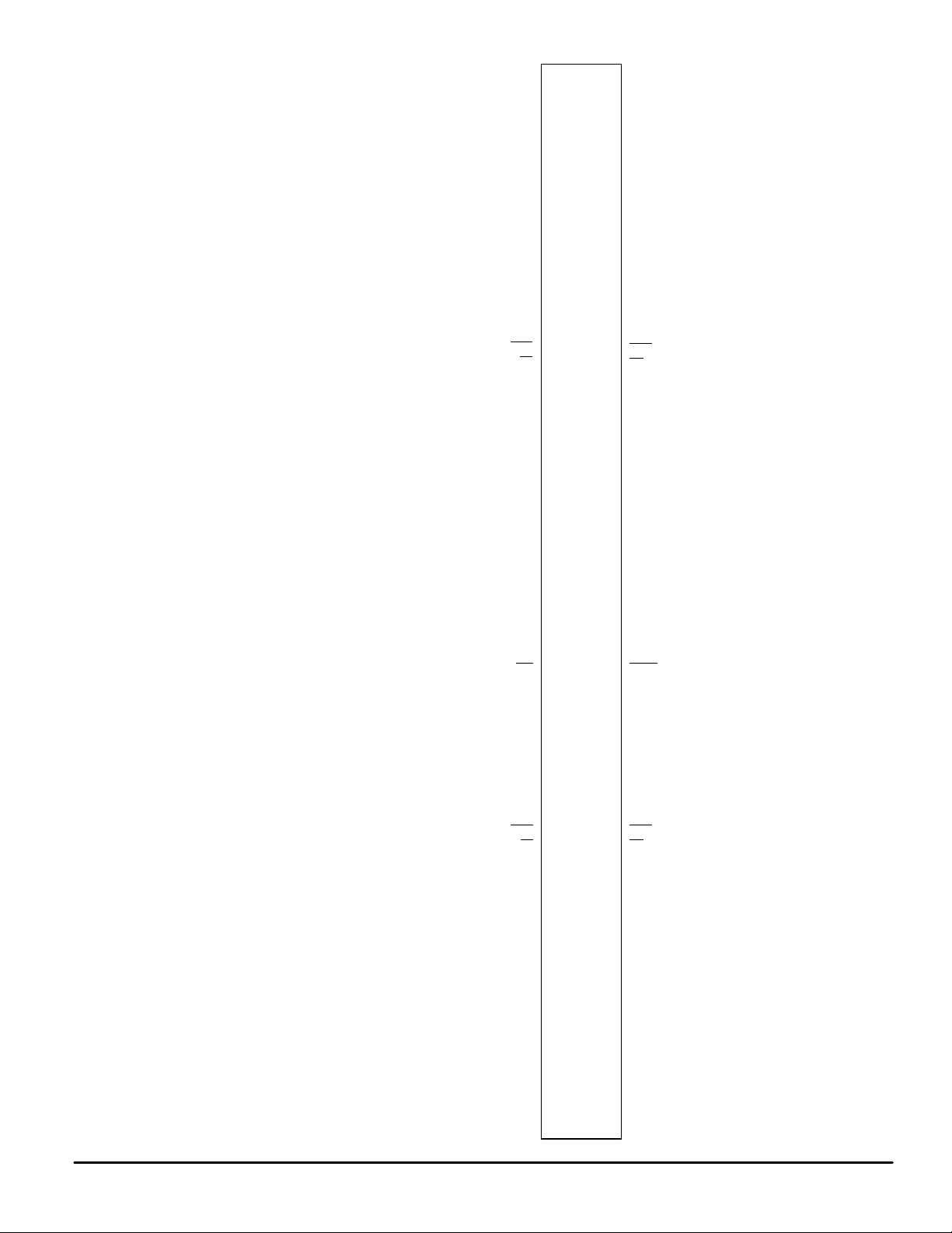
PIN ASSIGNMENT
144–LEAD DIMM
TOP VIEW
V
SS
A0
A2
A4
V
DD
NC
NC
V
SS
A6
A8
A10
NC
V
DD
A12
A14
A16
V
SS
PD0
V
SS
BW0
E0
V
SS
K1
V
SS
DQ0
V
DD
DQ2
DQ4
DQ6
V
SS
V
DD
DQ8
DQ10
V
SS
DQ12
DQ14
DP0
NC
NC
V
SS
WE
NC
V
DD
NC
NC
NC
V
DD
NC
NC
NC
V
SS
BW2
E1
V
DD
DQ16
DQ18
NC
NC
NC
V
SS
K3
V
SS
DQ20
V
SS
DQ22
DQ24
DQ26
DQ28
V
DD
DQ30
DP2
V
SS
1
3
5
7
9
11
13
15
17
19
21
23
25
27
29
31
33
35
37
39
41
43
45
47
49
51
53
55
57
59
61
63
65
67
69
71
73
75
77
79
81
83
85
87
89
91
93
95
97
99
101
103
105
107
109
111
113
115
117
119
121
123
125
127
129
131
133
135
137
139
141
143
10
12
14
16
18
20
22
24
26
28
30
32
34
36
38
40
42
44
46
48
50
52
54
56
58
60
62
64
66
68
70
72
74
76
78
80
82
84
86
88
90
92
94
96
98
100
102
104
106
108
110
112
114
116
118
120
122
124
126
128
130
132
134
136
138
140
142
144
2
4
6
8
V
SS
A1
A3
A5
V
DD
NC
NC
V
SS
A7
A9
A11
NC
V
DD
A13
A15
A17
V
SS
PD1
V
SS
BW1
G0
V
SS
K0
V
SS
DQ1
V
DD
DQ3
DQ5
DQ7
V
SS
V
DD
DQ9
DQ11
V
SS
DQ13
DQ15
DP1
NC
NC
V
SS
ADSP
NC
V
DD
NC
NC
NC
V
DD
NC
NC
NC
V
SS
BW3
G1
V
DD
DQ17
DQ19
NC
NC
NC
V
SS
K2
V
SS
DQ21
V
SS
DQ23
DQ25
DQ27
DQ29
V
DD
DQ31
DP3
V
SS
MCM36F8•MCM36F9
4
MOTOROLA FAST SRAM
 Loading...