

Motorola MCM321024SG20, MCM321024SG25 Datasheet
MOTOROLA
SEMICONDUCTOR TECHNICAL DATA
Advance Information
Order this document
by MCM321024/D
MCM321024
1M x 32 Bit
Fast Static RAM Module
The MCM321024 is an 32M bit static random access memory module organized as 1,048,576 words of 32 bits. The module is a 72–lead single in–line
memory module (SIMM) consisting of eight MCM6249 fast static RAMs packaged in 32–lead SOJ packages and mounted on a printed circuit board along with
sixteen decoupling capacitors.
The MCM6249 is a high performance CMOS fast static RAM organized as
1,048,576 words of 4 bits. Static design eliminates the need for external clocks
or timing strobes, while CMOS circuitry reduces power consumption and provides for greater reliability .
The MCM321024 is equipped with output enable (G
enable (E1 – E4) inputs, allowing for greater system flexibility . The G input, when
high, will force the outputs to high impedance. Ex
PD0 – PD3 are reserved for density identification. PD0 and PD2 are connected
to ground. These pins can be used to identify the density of the memory module.
• Single 5 V ± 10% Power Supply
• Fast Access Time: 20/25 ns
• Three–State Outputs
• Fully TTL Compatible
• JEDEC Standard Pinout
• Power Requirement: 1520/1400 mA Maximum, Active AC
• High Board Density SIMM Package
• Byte Operation: Four Separate Chip Enables, One for Each Byte (Eight Bits)
• High Quality Six–Layer FR4 PWB with Separate Internal Power and
Ground Planes
• Incorporates Motorola’s State–of–the–Art Fast Static RAMs
PIN NAMES
A0 – A19 Address Inputs. . . . . . . . . . . . . . . . . . . . . . . . . . .
W
G
E1
– E4 Byte Enables. . . . . . . . . . . . . . . . . . . . . . . . . . . . . .
DQ0 – DQ31 Data Input/Output. . . . . . . . . . . . . . . . . . . . . .
V
CC
V
SS
PD0 – PD3 Package Density. . . . . . . . . . . . . . . . . . . . . . . .
NC No Connect. . . . . . . . . . . . . . . . . . . . . . . . . . . . . . . . . . .
For proper operation of the device, VSS must be connected
to ground.
) and four separate byte
high will do the same for byte x.
Write Enable. . . . . . . . . . . . . . . . . . . . . . . . . . . . . . . . . . .
Output Enable. . . . . . . . . . . . . . . . . . . . . . . . . . . . . . . . . .
+ 5 V Power Supply. . . . . . . . . . . . . . . . . . . . . . . . . . .
Ground. . . . . . . . . . . . . . . . . . . . . . . . . . . . . . . . . . . . . .
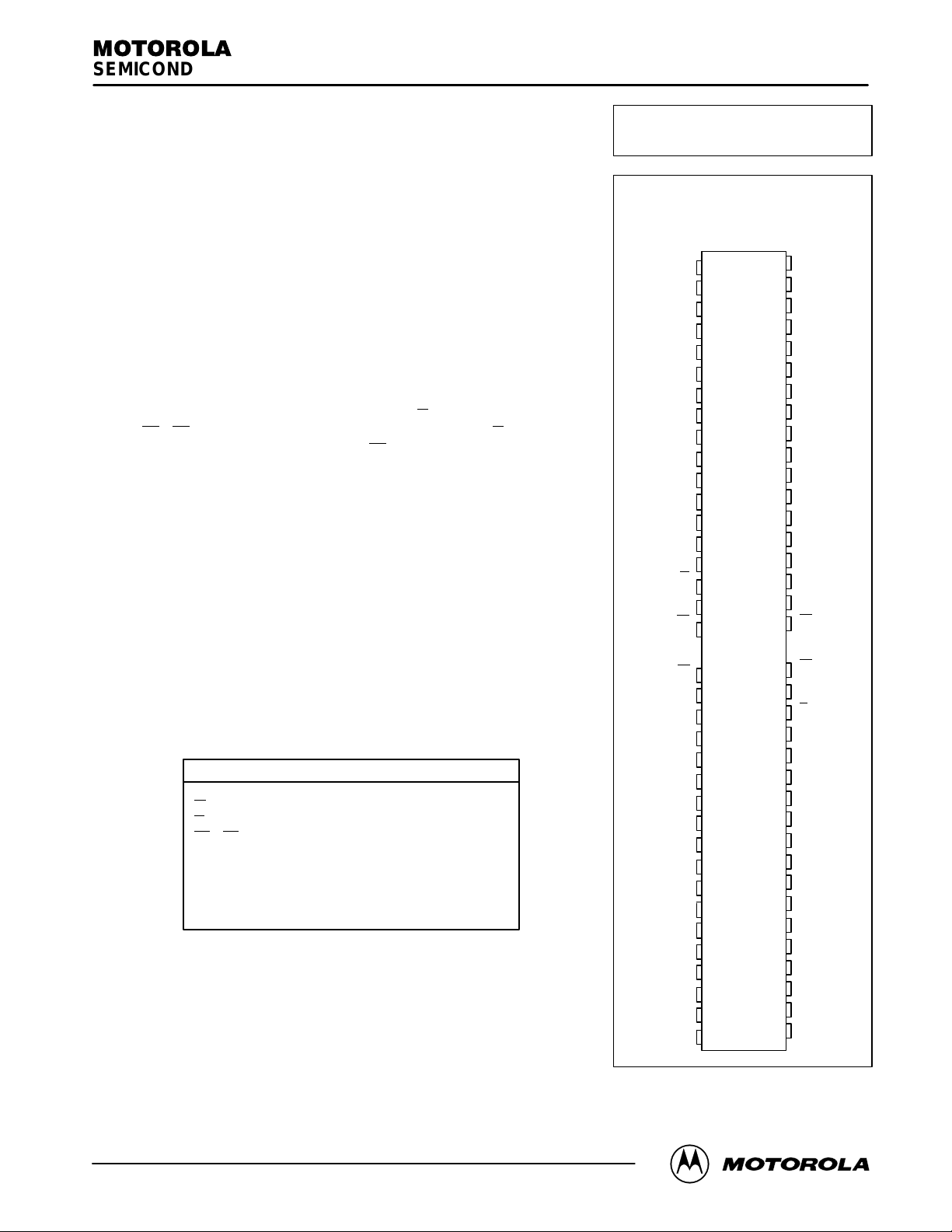
PIN ASSIGNMENT
TOP VIEW
72 LEAD SIMM — CASE TBD
1
11
13
15
17
19
21
23
25
27
29
31
33
35
37
39
41
43
45
47
49
51
53
55
57
59
61
63
65
67
69
71
NC
3
PD2
V
5
SS
7
PD1
DQ8
9
DQ9
DQ10
DQ11
A0
A1
A2
DQ12
DQ13
DQ14
DQ15
V
SS
A15
E2
E4
A17
G
DQ24
DQ25
DQ26
DQ27
A3
A4
A5
V
CC
A6
DQ28
DQ29
DQ30
DQ31
A18
NC
NC
PD3
PD0
DQ0
DQ1
DQ2
DQ3
V
CC
A7
A8
A9
DQ4
DQ5
DQ6
DQ7
W
A14
E1
E3 38
A16
V
SS
DQ16
DQ17
DQ18
DQ19
A10
A11
A12
A13
DQ20
DQ21
DQ22
DQ23
V
SS
A19
NC
2
4
6
8
10
12
14
16
18
20
22
24
26
28
30
32
34
36
40
42
44
46
48
50
52
54
56
58
60
62
64
66
68
70
72
This document contains information on a new product. Specifications and information herein are subject to change without notice.
REV 1
11/15/96
Motorola, Inc. 1996
MOTOROLA FAST SRAM
MCM321024
1
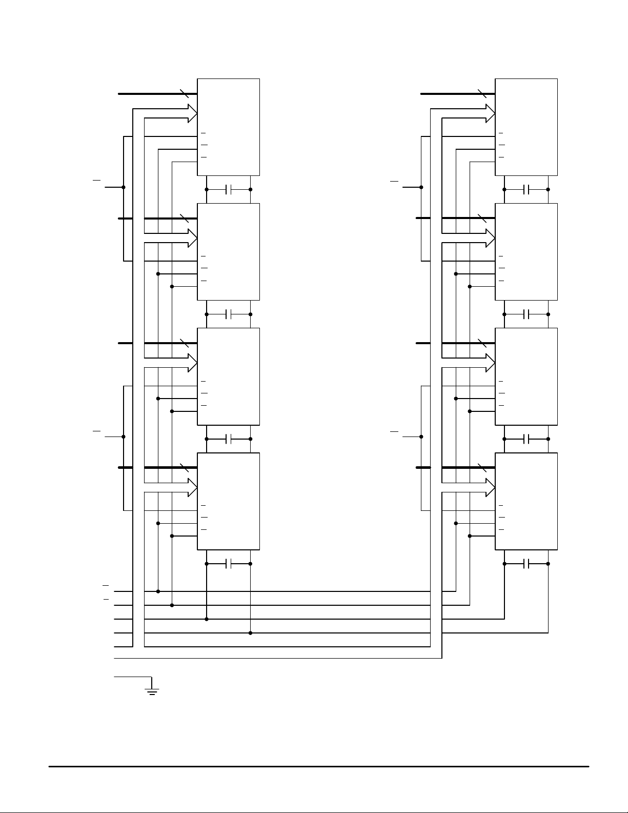
FUNCTIONAL BLOCK DIAGRAM
1M x 32 MEMORY MODULE
DQ0 – DQ3
E1
DQ4 – DQ7
DQ8 – DQ11
4
4
4
DQ0 – DQ3
A0 – A19
E
W
G
DQ0 – DQ3
A0 – A19
E
W
G
DQ0 – DQ3
A0 – A19
DQ16 – DQ19
E3
DQ20 – DQ23
DQ24 – DQ27
4
DQ0 – DQ3
A0 – A19
E
W
G
4
DQ0 – DQ3
A0 – A19
E
W
G
4
DQ0 – DQ3
A0 – A19
E2
DQ12 – DQ15
W
G
V
CC
V
SS
A0 – A19
PD0, PD2
E
W
G
4
DQ0 – DQ3
A0 – A19
E
W
G
PD1, PD3 – OPEN
E4
DQ28 – DQ31
E
W
G
4
DQ0 – DQ3
A0 – A19
E
W
G
MCM321024
2
MOTOROLA FAST SRAM
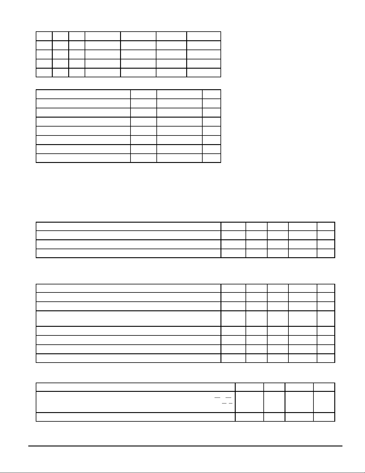
TRUTH TABLE
Ex G W Mode VCC Current Output Cycle
H X X Not Selected I
L H H Read I
L L H Read I
L X L Write I
SB1
or I
CCA
CCA
CCA
SB2
High–Z —
High–Z —
D
out
D
in
Read Cycle
Write Cycle
ABSOLUTE MAXIMUM RATINGS (Voltages referenced to V
Rating
Power Supply Voltage V
Voltage Relative to V
Output Current (per I/O) I
Power Dissipation P
Temperature Under Bias T
Operating Temperature T
Storage Temperatrue T
NOTE: Permanent device damage may occur if ABSOLUTE MAXIMUM RA TINGS are ex-
ceeded. Functional operation should be restricted to RECOMMENDED OPERATING CONDITIONS. Exposure to higher than recommended voltages for extended
periods of time could affect device reliability .
SS
Symbol Value Unit
CC
Vin, V
out
bias
stg
– 0.5 to VCC + 0.5 V
out
D
A
= 0 V)
SS
– 0.5 to 7.0 V
± 30 mA
8.0 W
– 10 to + 85 °C
0 to + 70 °C
– 25 to + 125 °C
DC OPERA TING CONDITIONS AND CHARACTERISTICS
(VCC = 5.0 V ± 10%, TA = 0 to + 70°C, Unless Otherwise Noted)
RECOMMENDED OPERATING CONDITIONS
Parameter
Supply Voltage (Operating Voltage Range) V
Input High Voltage V
Input Low Voltage V
*VIH (max) = VCC + 0.3 V dc; VIH (max) = VCC + 2 V ac (pulse width ≤ 20 ns)
**VIL (min) = – 3.0 V ac (pulse width ≤ 20 ns)
(Voltages Referenced to VSS = 0 V)
The devices on this module contain circuitry
to protect the inputs against damage due to
high static voltages or electric fields; however,
it is advised that normal precautions be taken
to avoid application of any voltage higher than
maximum rated voltages to these high impedance circuits.
These CMOS memory circuits have been
designed to meet the dc and ac specifications
shown in the tables, after thermal equilibrium
has been established. The module is in a test
socket or mounted on a printed circuit board
and transverse air flow of at least 500 linear
feet per minute is maintained.
Symbol Min Typ Max Unit
CC
IH
IL
4.5 5.0 5.5 V
2.2 — VCC+0.3* V
– 0.5** — 0.8 V
DC CHARACTERISTICS
Parameter Symbol Min Typ Max Unit
Input Leakage Current (All Inputs, Vin = 0 to VCC) I
Output Leakage Current (G, Ex = VIH, V
AC Active Supply Current (G, Ex = VIL, I
Cycle time ≥ t
AC Standby Current (Ex = VIH, Cycle time ≥ t
CMOS Standby Current (Ex ≥ VCC – 0.2 V, All Inputs ≥ VCC – 0.2 V or ≤ 0.2 V) I
Output Low Voltage (IOL = + 8.0 mA) V
Output High Voltage (IOH = – 4.0 mA) V
NOTE: Good decoupling of the local power supply should always be used.
min) MCM321024–25: t
AVAV
CAPACITANCE (f = 1.0 MHz, dV = 3.0 V, T
Input Capacitance (All pins except DQ0 – DQ31, W, G, and E1 – E4)
Input/Output Capacitance (DQ0 – DQ31) C
= 0 to VCC) I
out
= 0 mA, MCM321024–20: t
out
min) I
AVAV
= 25°C, Periodically Sampled Rather Than 100% Tested)
A
Characteristic
AVAV
AVAV
= 20 ns
= 25 ns
E1
– E4
W, G
lkg(I)
lkg(O)
I
CCA
SB1
SB2
OL
OH
— — ± 8 µA
— — ± 8 µA
—
—
— 400 480 mA
— 80 120 mA
— — 0.4 V
2.4 — — V
Symbol Typ Max Unit
C
in
out
1440
1320
32
10
40
8 9 pF
1520
1400
48
14
64
mA
pF
MOTOROLA FAST SRAM
MCM321024
3
 Loading...