

Motorola MCM101525TB15, MCM101525TB12 Datasheet
MCM101525
1
MOTOROLA FAST SRAM
Product Preview
2M x 2 Bit Fast Static
Random Access Memory with
ECL I/O
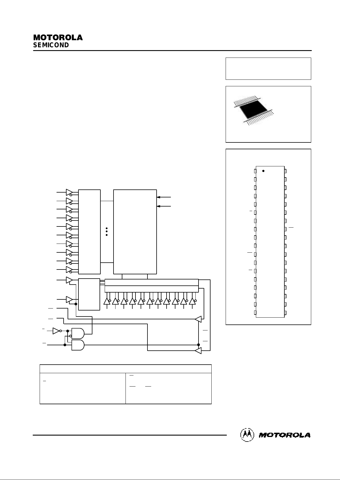
The MCM101525 is a 4,194,304 bit static random access memory organized
as 2,097,152 words of 2 bits. This device features complementary outputs. This
circuit is fabricated using high performance silicon–gate BiCMOS technology.
Asynchronous design eliminates the need for external clocks or timing strobes.
The MCM101525 is available in a 400 mil, 36 lead TAB.
• Fast Access Times: 12, 15 ns
• Equal Address and Chip Select Access Time
• Power Operation: – 195 mA Maximum, Active AC
BLOCK DIAGRAM
ROW
DECODER
MEMORY MATRIX
1024 ROWS x
4096 COLUMNS
INPUT
DATA
CONTROL
COLUMN I/O
COLUMN DECODER
A15
A14
A13
A12
A11
A10
A9
A8
A18 A5 A3 A1
S
W
A16
A7 A6 A4 A2
Q0
Q0
Q1
Q1
A17
A0
D1
Q0
Q0
Q1
Q1
V
CC
V
EE
A20 A19
D0
A0 – A20 Address Inputs W Write Enable. . . . . . . . . . . . . . . . . . . . . . . . . . . . . . . . . .
S
Chip Select D0 – D1 Data Input. . . . . . . . . . . . . . . . . . . . . . . . . . . . . . . . . . . . . . . . .
Q0 – Q1 Data Output Q0
and Q1 Complementary Data Out. . . . . . . . . . . . . . . . . .
NC No Connection V
EE
Power Supply. . . . . . . . . . . . . . . . . . . . . . . . . . . . . . . . . . . .
V
CC
Ground. . . . . . . . . . . . . . . . . . . . . . . .
PIN NAMES
This document contains information on a new product under development. Motorola reserves the right to change or discontinue this product without notice.
Order this document
by MCM101525/D
MOTOROLA
SEMICONDUCTOR TECHNICAL DATA
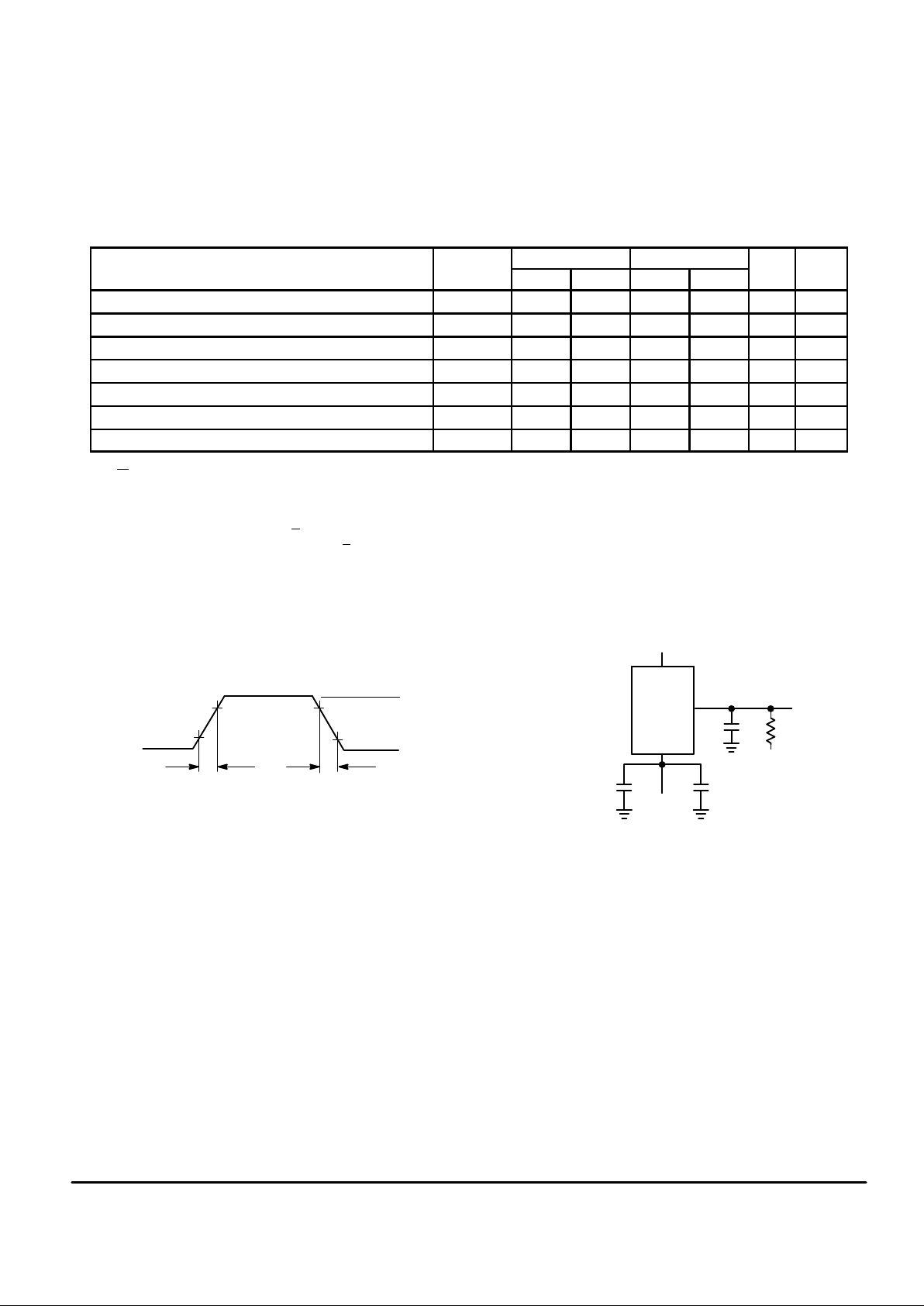
PIN ASSIGNMENT
MCM101525
5
4
3
2
1
10
9
8
7
6
11
12
13
14
15
16
17
18
20
21
22
23
24
25
26
19
27
28
32
31
30
29
36
35
34
33
A13
A12
A11
A10
S
A14
V
EE
V
CC
Q0
D0
Q0
A15
A0
W
A17
A16
A18
V
CC
Q1
D1
NC
A9
A4
A5
A6
A7
V
EE
A3
A8
A19
NC
A20
Q1
A1
A2
TB PACKAGE
400 MIL TAB
CASE 984A–01
V
EE
Motorola, Inc. 1994
8/94
MCM101525
2
MOTOROLA FAST SRAM
TRUTH TABLE (X = Don’t Care)
S
W Operation Data Output Current
H X Not Enabled X L —
L H Read X Q/Q I
EE
L L Write X L I
EE
ABSOLUTE MAXIMUM RATINGS (See Note)
Rating
Symbol Value Unit
VEE Pin Potential (to Ground) V
EE
– 7.0 to + 0.5 V
Voltage Relative to VCC for Any Pin
Except V
EE
Vin, V
outVEE
– 0.5 to+ 0.5 V
Output Current (per I/O) I
out
– 50 mA
Power Dissipation P
D
2.0 W
Temperature Under Bias T
bias
– 30 to + 85 °C
Operating Temperature T
J
0 to + 60 °C
Storage Temperature — Plastic T
stg
– 55 to + 125 °C
NOTE:Permanent device damage may occur if ABSOLUTE MAXIMUM RATINGS are
exceeded. Functional operation should be restricted to the OPERATING CONDITIONS. Exposure to higher than recommended voltages for extended periods of time
could affect device reliability.
DC OPERATING CONDITIONS AND CHARACTERISTICS
(VCC = 0 V, VEE = – 5.2 V ± 5%, TJ = 0 to + 60°C, Unless Otherwise Noted)
DC OPERATING CONDITIONS AND SUPPLY CURRENTS
Parameter Symbol Min Typ Max Unit
Supply Voltage (Operating Voltage Range) V
EE
– 5.46 – 5.2 – 4.94 V
Input High Voltage V
IH
– 1165 — – 880 mV
Input Low Voltage V
IL
– 1810 — – 1475 mV
Output High Voltage V
OH
– 1025 — – 880 mV
Output Low Voltage V
OL
– 1810 — – 1620 mV
Input Low Current I
IL
– 50 — — µA
Input High Current I
IH
— — 220 µA
Chip Select Input Low Current I
IL(CS)
0.5 — 170 µA
Operating Power Supply Current: tAVAV = 20 ns (All Outputs Open)* I
EE
— — – 195 mA
Quiescent Power Supply Current: fo = 0 MHz (Outputs Open) I
EEQ
— — – 150 mA
Voltage Compensation (VOH) ∆VOH/∆V
EE
± 35 mV/V @ – 4.94 to – 5.46 V
Voltage Compensation (VOL) ∆VOL/∆V
EE
± 60 mV/V @ – 4.94 to – 5.46 V
*Address Increment
RISE/FALL TIME CHARACTERISTICS
Parameter Symbol Test Condition Min Typ Max Unit
Output Rise Time t
r
20% to 80% 0.5 1.0 1.5 ns
Output Fall Time t
f
20% to 80% 0.5 1.0 1.5 ns
CAPACITANCE (f = 1.0 MHz, T
A
= 25°C, Periodically Sampled Rather Than 100% Tested)
Parameter
Symbol Typ Max Unit
Input Capacitance Address and Data
S
, W
C
in
C
ck
3.5
4
7
7
pF
Output Capacitance Q, Q C
out
4 8 pF
This device contains circuitry to protect
the inputs against damage due to high static
voltages or electric fields; however, it is advised that normal precautions be taken to
avoid application of any voltage higher than
maximum rated voltages to these high
impedance circuits.
This BiCMOS memory circuit has been
designed to meet the dc and ac specifications shown in the tables, after thermal equilibrium has been established. The circuit is
in a test socket or mounted on a printed circuit board and transverse air flow of at least
500 linear feet per minute is maintained.
MCM101525
3
MOTOROLA FAST SRAM
AC OPERATING CONDITIONS AND CHARACTERISTICS
(VEE = – 5.2 V ± 5%, VCC = 0 V, TJ = 0 to +60°C, Unless Otherwise Noted)
Input Pulse Levels – 1.7 V to – 0.9 V (See Figure 1). . . . . . . . . . . . .
Input Rise/Fall Time 1 ns. . . . . . . . . . . . . . . . . . . . . . . . . . . . . . . . . . . .
Input Timing Measurement Reference Level 50%. . . . . . . . . . . . . . . .
Output Timing Measurement Reference Level VOH = – 1165 mV. .
VOL = – 1475 mV
Output Load (AC Test Circuit) See Figure 2. . . . . . . . . . . . . . . . . . . . .
READ CYCLE TIMING (See Notes 1 and 2)
MCM101525–12 MCM101525–15
Parameter Symbol Min Max Min Max Unit Notes
Read Cycle Time t
AVAV
12 — 15 — ns 2, 3
Address Access Time t
AVQV
— 12 — 15 ns
Chip Select Access Time t
SLQV
— 12 — 15 ns 6
Select High to Output Low t
SHQL
0 8 0 9 ns
Output Hold from Address Change t
AXQX
4 — 4 — ns
Power Up Time t
SLIEEH
0 — 0 — ns 4
Power Down Time t
SHIEEL
— 12 — 15 ns 4
NOTES:
1. W
is high for read cycle.
2. Product sensitivites to noise require proper grounding and decoupling of power supplies during read and write cycles.
3. All read cycle timings are referenced from the last valid address to the first transitioning address.
4. This parameter is sampled and not 100% tested.
5. Device is continuously selected (S
≤ VIL).
6. Addresses valid prior to or coincident with S
going low.
80%
Figure 1. Input Levels Figure 2. AC Test Circuit
AC TEST CONDITIONS
50%
20% 20%
50%
80%
– 0.9 V
– 1.7 V
t
f
t
r
V
CC
V
EE
Q
C
L
R
L
– 2.0 V
0.01
µ
F0.1 µF
tr = Rise Time
tf = Fall Time
50% = Timing Reference Levels
RL = 50
Ω
CL = 30 pF
 Loading...