

Motorola MCK12140D, MCH12140D Datasheet
Order this document By MCH12140/D
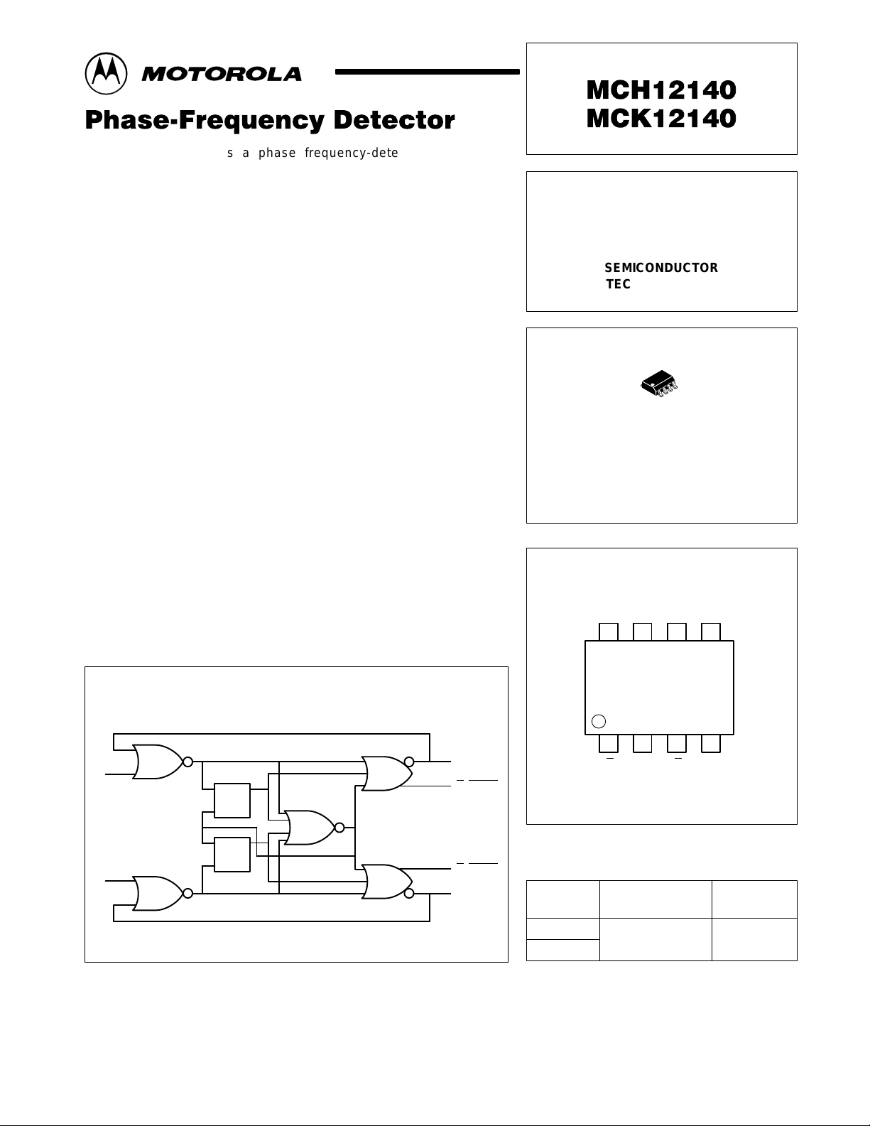
The MCH/K12140 is a phase frequency-detector intended for
phase-locked loop applications which require a minimum amount of phase
and frequency difference at lock. When used in conjunction with the
MC12147, MC12148 or MC12149 VCO, a high bandwidth PLL can be
realized. The device is functionally compatible with the MC12040
phase-frequency detector, however the MOSAIC III process is used to
push the maximum frequency to 800 MHz and significantly reduce the dead
zone of the detector. When the Reference (R) and VCO (V) inputs are
unequal in frequency and/or phase, the differential UP (U) and DOWN (D)
outputs will provide pulse streams which when subtracted and integrated
provide an error voltage for control of a VCO.
The device is packaged in a small outline, surface mount 8-lead SOIC
package. There are two versions of the device to provide I/O compatibility to
the two existing ECL standards. The MCH12140 is compatible with
MECL10H logic levels while the MCK12140 is compatible to 100K ECL
logic levels. This device can also be used in +5.0 V systems. Please refer to
Motorola Application Note AN1406/D, “Designing with PECL (ECL at +5.0
V)” for more information.
• 800 MHz Typical Bandwidth
• Small Outline 8-Lead SOIC Package
• 75 kΩ Internal Input Pulldown Resistors
• >1000 V ESD Protection
For proper operation, the input edge rate of the R and V inputs should be
less than 5ns.
MOSAIC III and MECL 10H are trademarks of Motorola
PHASE–FREQUENCY
DETECTOR
SEMICONDUCTOR
TECHNICAL DATA
8
1
D SUFFIX
PLASTIC PACKAGE
CASE 751
(SO–8)
PIN CONNECTIONS
R
V
LOGIC DIAGRAM
RQ
S
SQ
R
U (fR > fV)
U
(fR > fV)
D
(fV > fR)
D (fV > fR)
ORDERING INFORMATION
Device
MCH1214OD
MCK12140D
V
R
V
CC
8
7
1
2
U
U
(Top View)
Operating
Temperature Range
TA = –40° to +70°C SO–8
V
EE
6
5
3
4
D
D
Package
Motorola, Inc. 1997 Rev 4
MCH12140 MCK12140
TRUTH TABLE*
Input Output Input Output
R V U D U D R V U D U D
0
0
1
0
1
0
1
1
NOTE: * This is not strictly a functional table; i.e., it does not cover all possible modes of operation. However, it gives a sufficient number of tests to ensure that
the device will function properly.
H–SERIES DC CHARACTERISTICS (V
Output HIGH Voltage V
Output LOW Voltage V
Input HIGH Voltage V
Input LOW Voltge V
Input LOW Current I
NOTE: 1.10H circuits are designed to meet the DC specifications shown in the table after thermal equilibrium has been established. The circuit is in a test socket
K–SERIES DC CHARACTERISTICS (V
Output HIGH Voltage V
Output LOW Voltage V
Output HIGH Voltage V
Output LOW Voltage V
Input HIGH Voltage V
Input LOW Voltge V
Input LOW Current I
NOTE: 1.This table replaces the three tables traditionally seen in ECL 100K data books. The same DC parameter values at VEE = –4.5V now apply across the
ABSOLUTE MAXIMUM RATINGS (Note 1)
Power Supply (VCC = 0V) V
Input Voltage (VCC = 0V) V
Output Current Continuous
Operating Temperature Range T
Operating Range
NOTES: 1. Absolute maximum rating, beyond which, device life may be impaired, unless otherwise specified on an individual data sheet.
2.Parametric values specified at: H–Series: –4.20 V to –5.50 V
3.ESD data available upon request.
0
1
1
1
1
1
1
0
X
X
X
X
1
1
1
1
X
X
X
X
0
0
0
0
X
X
X
X
0
0
0
0
= VEE(min) – VEE(max); VCC = GND1, unless otherwise noted.)
EE
X
X
X
X
1
1
1
1
1
1
1
1
1
0
1
1
0
1
0
1
1
1
0
0
0
0
0
0
0
0
0
1
1
1
1
0
1
1
1
1
1
1
1
1
1
0
0
0
0
1
–40°C 0°C 25°C 70°C
Characteristic Symbol Min Max Min Max Min Max Min Max Unit
OH
OL
IL
or mounted on a printed circuit board and transverse airflow greater than 500lfpm is maintained. Outputs are terminated through a 50Ω resistor to –2.0V
except where otherwise specified on the individual data sheets.
–1080 –890 –1020 –840 –980 –810 –910 –720 mV
–1950 –1650 –1950 –1630 –1950 –1630 –1950 –1595 mV
–1230 –890 –1170 –840 –1130 –810 –1060 –720 mV
IH
–1950 –1500 –1950 –1480 –1950 –1480 –1950 –1445 mV
IL
0.5 — 0.5 — 0.5 — 0.3 — µA
= VEE(min) – VEE(max); VCC = GND1, unless otherwise noted.)
EE
–40°C 0°C to 70°C
Characteristic Symbol Min Typ Max Min Typ Max Unit Condition
OH
OL
OHA
OLA
IL
full VEE range of –4.2V to –5.5V. Outputs are terminated through a 50Ω resistor to –2.0V except where otherwise specified on the individual data
sheets.
Characteristic
Surge
1,2
K–Series: –4.94 V to –5.50 V
–1085 –1005 –880 –1025 –955 –880 mV VIN = VIH(max)
–1830 –1695 –1555 –1810 –1705 –1620 mV or VIL(min)
–1095 — — –1035 — — mV VIN = VIH(min)
— — –1555 — — –1610 mV or VIL(max)
IH
–1165 — –880 –1165 — –880 mV
–1810 — –1475 –1810 — –1475 mV
IL
0.5 — — 0.5 — — µA VIN = VIL(max)
Symbol Rating Unit
EE
I
I
out
A
V
EE
–8.0 to 0 VDC
0 to –6.0 VDC
50
mA
100
–40 to +70 °C
–5.7 to –4.2 V
2
MOTOROLA RF/IF DEVICE DATA
 Loading...