

Page 1

Advance Information
MCF5407PB/D
Rev. 3.3, 2/2003
Freescale Semiconductor, Inc.
MCF5407 Integrated
ColdFire
Product Brief
nc...
I
cale Semiconductor,
Frees
®
Microprocessor
This document is an overview of the MCF5407 ColdFire processor, focusing on feature
enhancements over the MCF5307. It includes general descriptions of features and of the
various modules incorporated in the MCF5407. It describes the V4 programming model as it
is implemented in the MCF5407.
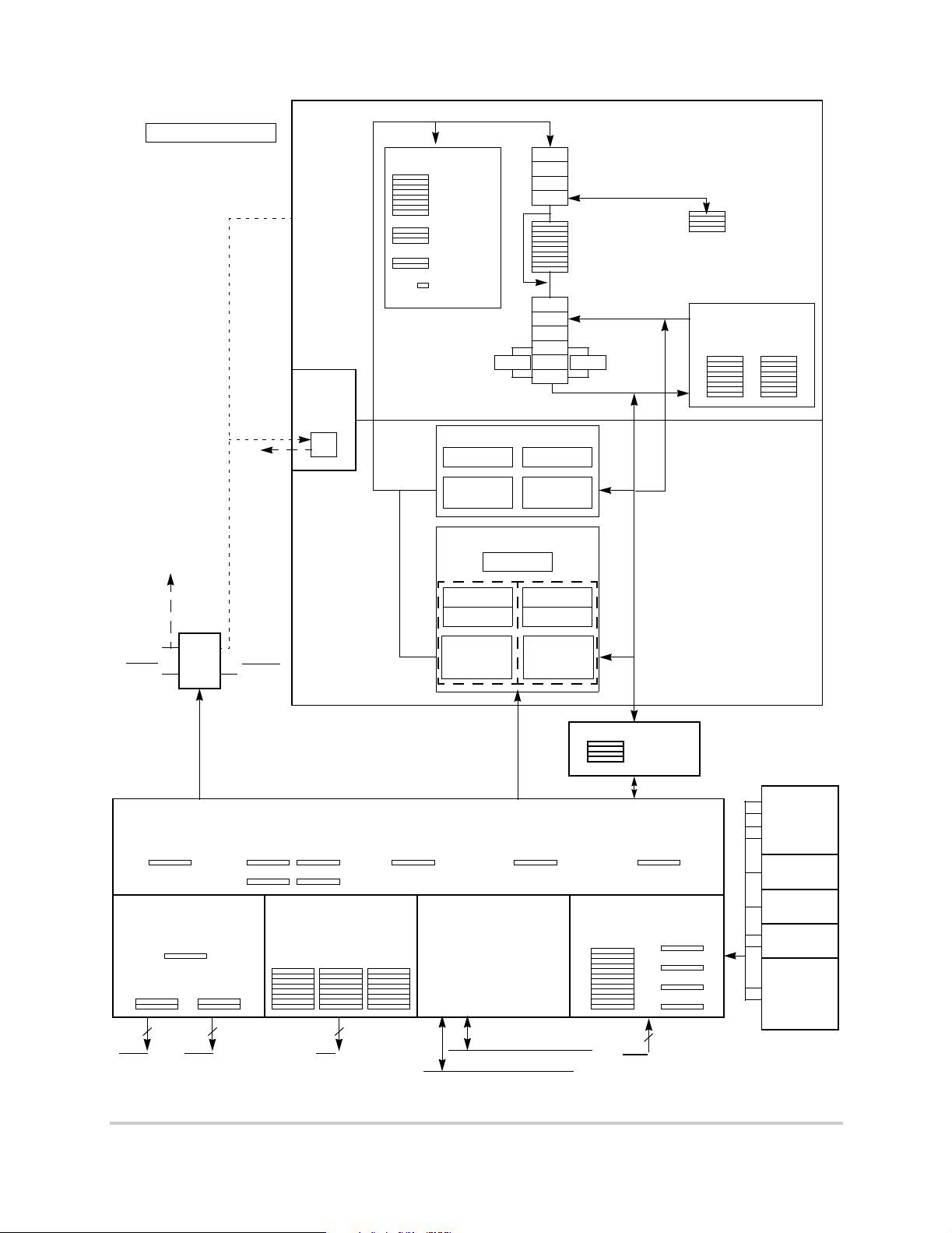
1.1 Features
The MCF5407 integrated mi cr opr ocessor combines a Version 4 ColdFire pr oce ss or core with
the following components, as shown in Figure 1:
• Harvard architecture memory system with 16-Kbyte instruction cache and 8-Kbyte
data cache
• Two, 2-Kbyte on-chip SRAMs
• Integer/fractional multiply-accumulate (MAC) unit
• Divide unit
• System debug interface
• DRAM controller for synchronous and asynchronous DRAM
• Four-channel DMA controller
• Two general-purpose timers
• Two UARTs, one that supports synchronous operations
2C™
•I
• Parallel I/O interface
• System integration module (SIM)
Designed for embedded control applications, the MCF5407 delivers 316 Dhrystone MIPS at
220 MHz or 233 Dhrystone MIPS at 162 MHz.
interface
For More Information On This Product,
Go to: www.freescale.com
Page 2
Features
JTAG
Freescale Semiconductor, Inc.
Debug
Module
V4 COLDFIRE PROCESSOR COMPLEX
Instruction Fetch
DIV
IAG
Pipeline (IFP)
IC1
IC2
IED
Ten-Instruction
FIFO Buffer
Operand Execution
Pipeline (OEP)
DS
AG
OC1
OC2
MAC
EX
DA
Branch Logic
8-Entry
Branch
Cache
128-Entry
.
.
Prediction
.
Table
CCR
LIFO Return
Stack
General-
Purpose Registers
A0–A7 D0–D7
31 0 31 0
nc...
I
cale Semiconductor,
Frees
CLKIN
(to on-chip
peripherals)
CLKIN
RSTI
PLL
PLL
Xn
PSTCLK
PCLK
RSTO
System Control PLL Control
RSR
÷2
Instruction Bus
SYSTEM INTEGRATION MODULE (SIM)
Base Address
SWIVR
SWSR SYPCR
MBAR
SRAM Controller
RAMBAR0
2-Kbyte
SRAM0
Harvard Cache Controller
ACR2 ACR0
ACR3 ACR1
16-Kbyte
Instruction
Cache
RAMBAR1
2-Kbyte
SRAM1
CACR
8-Kbyte
Bus Master Park
MPARK
Data
Cache
31 0
Local Memory Local Memory
Data Bus
4-Entry
Store
Buffer
Parallel Port
PLL
DMA
Four
Channels
Software
Watchdog
DRAM Controller Chip-Selec t Module External
DRAM Control
DCR
Addr/Cntrl Mask
DMR0/1DACR0/1
4
RAS[1:0]2CAS[3:0]
888
CSARs CSCRs CSMRs
8
CS[7:0]
Bus Interface
32-Bit Data Bus
32-Bit Address Bus
Interrupt Controller
12 ICRs
IRQP AR
IPR
IMR
AV R
4
IRQ[1,3,5,7]
I2C Module
Two UARTs
Two
General-
Purpose
Timers
Figure 1. MCF5407 Block Diagram
2 MCF5407 Integrated ColdFire® Microprocessor Product Brief MOTOROLA
For More Information On This Product,
Go to: www.freescale.com
Page 3

Freescale Semiconductor, Inc.
Although the MCF5407 offers obvious performance upgrade advantages, its rich memory and peripheral
integration at inexpensive prices should not be overlooked. Features common to many embedded
applications, such as DMAs, various DRAM controller interfaces, and on-chip memories, are integrated in
a cost-effective manner using aggressive process technologies.
The MCF5407 extends the legacy of Motorola’s 68K family by providing a compatible path for 68K and
ColdFire customers in which dev elopment tools and customer code ar e quickly leveraged. In fa ct, customers
moving from 68K to ColdFire can use code translation and emulation tools that facilitate modifying 68K
assembly code to the ColdFire architecture. The package, pinout, and integration mix of the MCF5407
create an especially simpl e upgrade for curre nt MCF5307 des igns wit h over trip le the sys tem perfor mance.
The revolutionary ColdFire microprocessor architecture provides new levels of price and performance to
cost-sensitive markets. Based on the concept of variable-length RISC technology, the ColdFire family
combines the architectural simplicity of conventional 32-bit RISC with a memory-saving, variable-length
instruction set. In defining the ColdFire architecture for embedded processing applications, a 68K-code
compatible core was created that combines the performance advantages of a RISC architecture with the
optimum code density of a streamlined, variable-length M68000 instruction set.
MCF5407 Features
nc...
I
cale Semiconductor,
Frees
By using a variable-length instruction set architecture, embedded system designers using ColdFire RISC
processors enjoy significant advantages over conventional fixed-length RISC architectures. The denser
binary code for ColdFire processors consumes less memory than many fixed-length instruction set RISC
processors available. This improved code density means more efficient system memory use for a given
application, and allows use of slower, less costly memory to help achieve a target performance level.
The MCF5407 is the first standard product to implement the Version 4 ColdFire microprocessor core. The
V4 microarchitecture implements a number of advanced techniques, including a Harvard memory
architecture, branc h cache acceleration l ogic, and limited superscal ar support (dual-instr uction issue), which
contribute to the 316 Dhrystone MIPS performance level. Increasing the internal speed of the core also
allows higher performance while providing the system designer with an easy-to-use lower speed system
interface. The processor complex frequency is an integer multiple, 3 to 6 times, of the external bus
frequency. The core clock can be stopped to support a low-power mode in the MCF5407.
Serial communication channels are provided by two programmable full-duplex UARTs, one of which
provides synchronous communications for soft-modem applications, and an I
channels of DMA allow for fast data transfer using a programmable burst mode independent of processor
execution. The two 16-bit general -purpose mult imode timers pro vide separat e input and output signals. For
system protection, the processor includes a programmable 16-bit software watchdog timer. In addition,
common system functions s uch as chip sele cts, inte rrupt cont rol, bus ar bitrati on, and an IEEE 1149.1 JTAG
module are included.
A sophisticated debug interface supports background-debug mode plus real-time trace and debug with an
expanded set of on- chip b reakpoi nt r egisters . Thi s int erfa ce is presen t in a ll Col dFire s tanda rd prod ucts a nd
allows common emulator support across the entire family of microprocessors.
2
C interface module. Four
1.2 MCF5407 Features
The following list summarizes MCF5407 features:
• ColdFire processor core
— Variable-length RISC, clock-multiplied Version 4 microprocessor core
— Implements Revision B of the ColdFire instruction set architecture (ISA), which leverages the
68K programming model
MOTOROLA MCF5407 Integrated ColdFire® Microprocessor Produc t Brief 3
For More Information On This Product,
Go to: www.freescale.com
Page 4

Freescale Semiconductor, Inc.
MCF5407 Features
— Two independent decoupled pipelines: four-stage instruction fetch pipeline (IFP) and
five-stage operand execution pipeline (OEP)
— Ten-instruction FIFO buffer provides decoupling between the pipelines
— Limited superscalar design achieves performance levels close to dual-issue performance
— Programmable two-level branch acceleration mechanism with an 8-entry branch cache plus a
128-entry prediction table for increased performance
— 32-bit internal address bus supporting 4 Gbytes of linear address space
— 32-bit data bus
— 16 user-accessible, 32-bit-wide, general-purpose registers
— Supervisor/user modes for system protection
— Vector base register to reloc ate exception-vector ta ble
— Optimized for high-level language constructs
• Multiply and accumulate unit (MAC)
nc...
I
cale Semiconductor,
Frees
— Provides high-speed, complex arithmetic processing for DSP applications
— Tightly coupled to the OEP
— Three-stage execute pipeline with one clock issue rate for 16 x 16 operations
— Supports 16 x 16 and 32 x 32 multiplies, all with 32-bit accumulate
— Supports signed or unsigned integers, plus signed fractional operands
• Hardware integer divide unit
— Supports unsigned and signed integer divides
— Tightly coupled to the OEP
— Supports 32/16, and 32/32 operations producing quotient and/or remainder results
• 16-Kbyte instruction cache, 8-Kbyte data cache
— Four-way set-associative organization
— Operates at higher processor core frequency
— Provides pipelined, single-cycle access to critical code and data
— Data cache supports write-through and copyback modes
— Four-entry, 32-bit store buffer to improve performance of operand writes
• Two, 2-Kbyte SRAMs
— Programmable location anywhere within 4-Gbyte linear address space
— Operates at higher core frequency
— Provides pipelined, single-cycle access to critical code and/or data
— Each block can be mapped to either the instruction or data operand bus
• DMA controller
— Four fully-programmable channels: two support external requests and external acknowledges
— Supports dual-address and single-address transfers with 8-, 16-, and 32-bit data capability
— Source/destination address pointers that can increment or remain constant
— 24-bit transfer counter per channel
4 MCF5407 Integrated ColdFire® Microprocessor Product Brief MOTOROLA
For More Information On This Product,
Go to: www.freescale.com
Page 5

Freescale Semiconductor, Inc.
— Operand packing and unpacking supported
— Auto-alignment transfers supported for efficient block movement
— Supports bursting and cycle steal
— Provides two bus clock internal access
— Automatic DMA transfers from on-chip UARTs using internal interrupts
• DRAM controller
— Support for synchronous DRAM (SDRAM), extended-data-out (EDO) DRAM, and fast page
mode
— Supports up to 512 Mbytes of DRAM
— Programmable timer provides CAS-before-RAS refresh for asynchronous DRAMs
— Support for two separate memory blocks
• Two UARTs
— One UART offers synchronous mode with expanded buffers for soft modem support
nc...
I
— Full-duplex operation
— Flexible baud-rate generator
MCF5407 Features
cale Semiconductor,
Frees
— Modem control signals available (CTS
— Processor-interrupt capability
• Dual 16-bit general-purpose multiple-mode timers
— 8-bit pre scaler
— Timer input and output pins
— Processor-interrupt capability
— Up to 18.5-nS resolution at 54 MHz
2
•I
C module
— Interchip bus interface for EEPROMs, LCD controllers, A/D converters, keypads
— Fully compatible with industry-s tandard I
— Master or slave modes support multiple masters
— Automatic interrupt generation with programmable level
• System interface module (SIM)
— Chip selects provide direct interface to 8-, 16-, and 32-bit SRAM, ROM, FLASH, and
memory-mapped I/O devices
— Eight, fully-programmable chip selects, each with a base address register
— Programmable wait states and port sizes per chip select
— User-programmable processor clock/input clock frequency ratio
, RTS)
2
C bus
— Programmable interrupt controller
— Low interr upt latency
— Four external interrupt request inputs
— Programmable autovector generator
— Software watchdog timer
MOTOROLA MCF5407 Integrated ColdFire® Microprocessor Produc t Brief 5
For More Information On This Product,
Go to: www.freescale.com
Page 6

Freescale Semiconductor, Inc.
ColdFire Module Description
• 16-bit general-purpose I/O interface
• IEEE 1149.1 test (JTAG) module
• System debug support
— Real-time trace for determining dynamic execution path while in emulator mode
— Background debug mode (BDM) for debug features while halted
— Real-time debug support, including 13 user-visible hardware breakpoint registers
— Supports servicing of critical, real-time interrupt requests while the BDM is in emulator mode
— Supports comprehensive emulator functions through trace and breakpoint logic
• On-chip PLL
— Accepts various clock input (CLKIN) frequencies between 25 and 54 MHz
— Supports core frequencies between 100 and 162 MHz
— Supports low-power mode
nc...
I
cale Semiconductor,
Frees
• Product offerings
— 316 Dhrystone MIPS at 220 MHz
— 233 Dhrystone MIPS at 162 MHz
— Implemented in 0.22 µ, quad-layer-metal process technology with 1.8-V operation (3.3-V
compliant I/O pads)
— 208-pin plastic QFP package
— 0 to 70° C operating temperature at 162 and 220 MHz
— -40 to 85° C operating temperature at 162 MHz
1.2.1 Process
The MCF5407 is manufactured in a 0. 22-µ CMOS process with quad-layer- metal routing technology. This
process combines the high performance and low power needed for embedded system applications. Inputs
are 3.3-V tolerant; outputs are CMOS or open-drain CMOS with outputs operating from VDD + 0.5 V to
GND - 0.5 V, with guaranteed TTL-level specifications.
1.3 ColdFire Module Description
The following sections provide overviews of the various modules incorporated in the MCF5407.
1.3.1 ColdFire Core
The Version 4 ColdFire core consists of two, independent and decoupled pipelines to maximize
performance—the instruction fetch pipeline (IFP) and the operand execution pipeline (OEP).
1.3.1.1 Instruction Fetch Pipeline (IFP)
The four-sta ge instructi on fetch pipeli ne (IFP) is designed to prefetch inst ructions for the operand execu tion
pipeline (OEP). Because the fetch and execution pipelines are decoupled by a ten-instruction FIFO buffer,
the fetch mechanism can prefetch instructions in advance of their use by the OEP, thereby minimizing the
6 MCF5407 Integrated ColdFire® Microprocessor Product Brief MOTOROLA
For More Information On This Product,
Go to: www.freescale.com
Page 7

Freescale Semiconductor, Inc.
time stalle d waitin g for in struc tions. To maximize the perf orman ce of c onditio nal bra nch in struct ions, th e
Version 4 IFP implements a sophisticated two-level acceleration mechanism.
The first level is an 8-entry, direct-mapped branch cache with a 2-bit prediction state (strongly/weakly,
taken/not-taken) for each entry. The branch cache implements instruction folding techniques that allow
conditional branch instructions which are predicted correctly as taken to execute in zero cycles.
For those conditional branches with no information in the branch cache, a second-level, direct-mapped
prediction table containing 128 entries is accessed. Again, each entry uses the same 2-bit prediction state
definition as the branc h cache. This branch predi ction state is then use d to predict the dire ction of prefetched
conditional branch instructions.
Other change-of-flow instructions, including unconditional branches, jumps, and subroutine calls, use a
similar mechanism where the IFP calculates the target address. The performance of subroutine return
instructions is improved through the use of a four-entry, LIFO return stack.
In all cases, these mechanisms allow the IFP to redirect the fetch stream down the path predicted to be taken
well in advance of the actual instruction execution. The net effect is significantly improved performance.
nc...
I
1.3.1.2 Operand Execution Pipeline (OEP)
ColdFire Module Description
cale Semiconductor,
Frees
The prefetched instruct ion stream is g ated from the FI FO buffer into the five-stage OE P. The OEP consists
of two, traditional two-stage RISC compute engines with a register file access feeding an arithmetic/logic
unit (ALU). The co mpute engin e located at the top of the OEP is typically used for operand memory address
calculations (the address ALU), while the compute engine located at the bottom of the pipeline is used for
instruction execution (the execution ALU). The resulting structure provides 3.9 Gbytes/S data operand
bandwidth at 162 MHz to the two compute engines and supports single-cycle execution speeds for most
instructions, including all load, store and most embedded-load operations. In response to users and
developers, the V4 desig n supports exec ution of the Co ldFire Revisi on B instructi on set, which ad ds a small
number of new instructions to improve performance and code density.
The OEP also implements two advanced performance features. It dynamically determines the appropriate
location of instruction execution (either in the address ALU or the execution ALU) based on the pipeline
state. The addre ss co mp ute e ngi ne, in conjunction wi th register renaming resources, can be use d t o exe cut e
a number of heavily-used opcodes and forward the results to subsequent instructions without any pipeline
stalls. Additionally, the OEP implements instruction folding techniques involving MOVE instructions so
that two instructions can be issued in a single machine cycle. The resulting microarchitecture approaches
the performance of a full superscalar implementation, but at a m uch lower silicon cost.
1.3.1.3 MAC Module
The MAC unit provides signal processing capabilities for the MCF5407 in a variety of applications
including digital audio and servo control. Integrated as an execution unit in the processor's OEP, the MAC
unit implements a three- stage arithmetic pi peline optimized f or 16 x 16 multiplies. Bot h 16- and 32-bit inpu t
operands are suppor ted by this design in addition t o a full s et of exte nsions for signed and unsigned in tegers
plus signed, fixed-point fractional input operands.
1.3.1.4 Integer Divide Module
Some embedded applications can benefit greatly from the integer divide unit. Integrated as another engine
in the processor’s OEP, the divide module performs a variety of operations using signed and unsigned
integers. The module supports word and longword divides producing quotients and/or remainders.
MOTOROLA MCF5407 Integrated ColdFire® Microprocessor Produc t Brief 7
For More Information On This Product,
Go to: www.freescale.com
Page 8

Freescale Semiconductor, Inc.
ColdFire Module Description
1.3.2 Harvard Architecture
A Harvard memory architecture is implemented to support the increased bandwidth requirements of the V4
processor pipelines. In this design featuring separate instruction and data buses to the processor-local
memories, available bandwidth to the processor reaches 1.3 Gbytes/S at 162 MHz and conflicts between
instruction fetches and operand accesses are removed.
1.3.2.1 16-Kbyte Instruction Cache/8-Kbyte Data Cache
Attached to the Harvard memory architecture are a 16-Kbyte instruction cache and an 8-Kbyte data cache.
These four-way, set-associative designs improve system performance by providing pipelined, single-cycle
access on instruction fetches and operand accesses that hit in these memories.
As with all ColdFire caches, these controllers implement a non-lockup, streaming design to maximize
performance. The use of processor-local memories decouples performance from external memory speeds
and increases available bandwidth for external devices or the on-chip 4-channel DMA.
nc...
I
cale Semiconductor,
Frees
Both caches implement line-fill buffers to optimize the performance of line-sized (16-byte) burst acc esses.
Additionally, the data cache supports operation of copyback, write-through or noncacheable modes. A
4-entry, 32-bit buffer is used for cache line push operations and can be configured for deferred write
buffering while in write-through or non-cacheable modes.
The new INTOUCH instruction can be used to prefetch instructions to be locked in the instruction cache
using the cache locking feature. This function may be desirable in certain systems where deterministic
real-time performance is critical.
1.3.2.2 Internal 2-Kbyte SRAMs
The two 2-Kbyte on-chip SRAM modules are also connected to the Harvard memory architecture, and
provide pipelined, si ngle-cyc le access to those me mory regions mapped to th ese device s. Each memory ca n
be independently mapped to any 0-modulo-2K location within the 4-Gbyte address space, and configured
to respond either to instruction or to data accesses. Time-critical functions can be mapped onto the
instruction memory bus, while the system stack and/or heavily-referenced data operands can be mapped
onto the data memory bus.
1.3.3 DRAM Controller
The MCF5407 DRAM controller pr ovid es a direct interface f or up t o t w o bl oc ks o f DRAM. The controller
supports 8-, 16-, or 32-bit memor y widths, and can easily interface to PC- 100 DIMMs. A unique addressing
scheme allows for increases in system memory size without rerouting address lines and rewiring boards.
The controller operates in normal mode or in page mode and supports SDRAMs and EDO DRAMs.
1.3.4 DMA Controller
The MCF5407 provides four fully-programmable DMA channels for quick data transfer. Dual- and
single-address mode s provide the abi lity to progra m bursting and cyc le steal. Dat a transfer s are 32 bits lo ng
with packing and unpacking supported along with an auto-alignment option for efficient block transfers.
Automatic block transfers from on-chip serial UARTs are also supported through the DMA channels.
8 MCF5407 Integrated ColdFire® Microprocessor Product Brief MOTOROLA
For More Information On This Product,
Go to: www.freescale.com
Page 9

Freescale Semiconductor, Inc.
ColdFire Module Description
1.3.5 UART Modules
The MCF5407 contains two UARTs, which function independently. One UART has been enhanced to
provide synchronous op eration and a CODEC in terface for s oft modem support. Ea ch UAR T can be cl ocked
by the system bus c lock, elimina ting the need f or an extern al crystal . Each UART module interfaces directly
to the CPU, as shown in Figure 2.
CTS
Serial Communications
Channel
RTS
RxD
TxD
16-Bit Timer for
Baud-Rate Generation
nc...
I
Each UART module consists of the following major functional a reas:
• Serial communication channel
• 16-bit timer for baud-rate generation
• Internal channel control logic
• Interrupt control logic
In addition, UART1 is enhanced to provide a CODEC interface for soft modem support. UART1 can be
programmed to function like UART0 or in one of three following modem modes:
cale Semiconductor,
• An 8-bit CODEC interface
• A 16-bit CODEC interface
• An audio CODEC ‘97 (AC97) digital interface controller
Internal Channel
Control Logic
Interrupt Control
Logic
Figure 2. UART Module Block Diagram
System bus clock
or
External clock (TIN)
Frees
Each UART contains an on-chip baud-rate generator, which provides both standard and nonstandard baud
rates. Data formats can be 5, 6, 7, or 8 bits with even, odd, or no parity, and up to 2 stop bits in 1/16
increments. The UARTs include the following transmit and receive FIFO b uffers:
• UART0 has a 4-byte FIFO receive buffer and a 2-byte FIFO transmit buffer.
• In UART1, the Tx and Rx FIFOs can hold the following:
— 32 1-byte samples when programmed as a UART or as an 8-bit CODEC interface
— 16 2-byte samples when programmed as a 16-bit CODEC interface
— 16 20-bit samples when programmed as a Digital AC ’97 Controller
The UART modules also provide several error-detection and maskable-interrupt capabilities. Modem
support includes request-to-send (RTS
MOTOROLA MCF5407 Integrated ColdFire® Microprocessor Produc t Brief 9
For More Information On This Product,
) and clear-to-send (CTS) lines.
Go to: www.freescale.com
Page 10

Freescale Semiconductor, Inc.
ColdFire Module Description
CLKIN provides the time base through a programmable pres caler . The UAR T time scale can al so be sourced
from a timer input. Full-duplex, auto-echo loopback, local loopback, and remote loopback modes allow
testing of UART connections. The programmable UARTs can interrupt the CPU on various normal or
error-condition events.
1.3.6 Timer Module
The timer module includes two general-purpose timers, each of which contains a free-running 16-bit timer
for use in any of three modes. One mode captures the timer value with an external event. Another mode
triggers an external signal or interrupts the CPU when the timer reaches a set value, while a third mode
counts external events.
The timer unit has a n 8-bit pres caler that allows prog ramming of the clock input frequency, which is derived
from the system bus cycle or an external clock input pin (TIN). The programmable timer-output pin
generates either an active-low pulse or toggles the output.
nc...
I
cale Semiconductor,
Frees
1.3.7 I2C Module
The I2C interface is a two-wire , bidirection al serial bus us ed for quick data exchanges between devices. The
2
I
C minimizes the interconnec tion between devic es in the end system and is best suited for appl ications tha t
need occasional bursts of rapid communication over short distances among several devices. The I
operate in master, slave or multiple-master m odes.
2
C can
1.3.8 System Interface
The MCF5407 processor provides a direct interface to 8-, 16-, and 32-bit FLASH, SRAM, ROM, and
peripheral devices through the use of fully-programmable chip selects and write enables. Support for burst
ROMs is also included. Through the on-chip PLL, users can input a slower clock (25 to 54 MHz) that is
internally multiplied to create the faster processor clock (100 to 162 MHz).
1.3.8.1 External Bus Interface
The bus interface controller transfers information between the ColdFire core or DMA, and memory,
peripherals, or ot her devices on t he external bus . The external bus interface provi des up to 32 bits of address
bus space, a 32-bit data bus, and all associated control signals. This interface implements an extended
synchronous protocol that supports bursting operations.
Simple two-wire request/acknowledge bus arbitration between the MCF5407 processor and another bus
master, such as an external DMA device, is glueless with arbitration logic internal to the MCF5407
processor. Multiple-master arbitration is also available with some simple external arbitration logic.
1.3.8.2 Chip Selects
Eight fully-programmable chip select outputs support the use of external memory and peripheral circuits
with user-defined wait-state insertion. These signals interface to 8-, 16-, or 32-bit ports. The base address,
access permissions, and internal bus transfer terminations are programmable wit h configuration regis ters for
each chip select. CS0
the MCF5407.
10 MCF5407 Integrated ColdFire® Microprocessor Product Brief MOTOROLA
also provides global chi p se lect functionality of boot ROM upon reset for init ia li zi ng
For More Information On This Product,
Go to: www.freescale.com
Page 11

Freescale Semiconductor, Inc.
ColdFire Module Description
1.3.8.3 16-Bit Parallel Port Interface
A 16-bit general-purpose programmable parallel port serves as either an input or an output on a pin-by-pin
basis.
1.3.8.4 Interrupt Controller
The interrupt controller provides user-programmable control of ten internal peripheral interrupts and
implements four external fixed interrupt-request pins. Each internal interrupt can be programmed to any one
of seven interrupt levels and four priority levels within each of these levels. Additionally, the external
interrupt request pi ns can b e mapped to levels 1, 3, 5, and 7 or level s 2, 4, 6, and 7. Autov ector c apabil ity i s
available f or both internal and external interrupts .
1.3.8.5 JTAG
To help with system diagnostics and manufacturing testing, the MCF5407 processor includes dedicated
user-acces si bl e te st logic that complies wit h t h e I EEE 1149.1a stan dar d fo r boundary-scan testab il it y, often
nc...
I
referred to as the Joint Test Action Group, or JTAG. For more information, refer to the IEEE 1149.1a
standard.
cale Semiconductor,
Frees
1.3.9 System Debug Interface
The ColdFire processor core debug interface is provided to support system debugging in conjunction with
low-cost debug and emulator development tools. Through a standard debug interface, users can access
real-time trace and debug information. This allows the processor and system to be debugged at full speed
without the need for costly in-circuit emulators. The debug unit contained in the MCF5407 is a compatible
upgrade to the MCF52xx an d MCF53xx debug modul es with added br eakpoint re gisters and s upport for I /O
interrupt request servicing while in em ulator mode.
The on-chip breakpoint resources include a total of 13 programmable registers—two sets of address
registers (each with two 32-bit registers), two sets of data registers (each with a 32-bit data register plus
32-bit data mask regist er) , one 32-bi t PC regi st er plus a 32-b it PC mask re gister and three additional 32- bi t
PC registers. These registers can be accessed through the dedicated debug serial communication channel,
or from the processor's supervisor mode programming model. The breakpoint registers can be configured
to generate triggers by combining the address, data and PC conditions in a variety of single or dual-level
definitions and t he trigger e vent can be pr ogrammed to gener ate a process or halt, or initiate a debu g interrupt
exception.
The MCF5407’s new interrupt servicing options during emulator mode allow real-time critical interrupt
service routines to be serviced while processing a debug interrupt event, thereby ensuring that the system
continues to operate even during debugging.
To support program trace, the Version 4 debug module has combined the processor status and debug data
outputs into a single 8-bit bus (PSTDDATA[7:0]). This bus along with the PSTCLK output provide
execution status, captured operand data and branch target addresses defining processor activity at one-half
the CPU's clock rate.
MOTOROLA MCF5407 Integrated ColdFire® Microprocessor Produc t Brief 11
For More Information On This Product,
Go to: www.freescale.com
Page 12

Freescale Semiconductor, Inc.
Programming Model, Addressing Modes, and Instruction Set
1.3.10 PLL Module
The MCF5407 PLL module is shown in Figure 3.
CLKIN (to on-chip peripherals)
BCLKO
nc...
I
cale Semiconductor,
Frees
CLKIN
DIVIDE[2:0]
RSTI
The PLL module’s three modes of operation (reset, normal, and reduced power) are described as follows.
• Reset mode—When RSTI
from the MCF5407. The core:bus frequency ratio along with other MCF5407 configuration
information are sampled during reset.
• Normal mode—In normal mode, the input frequency programmed at reset is clock-multiplied to
provide the processor clock (PCLK).
• Reduced-power mode—In reduced-power mode, the PCLK is disabled by executing a sequence
including programming a cont rol bit in the syst em configuration regi ster (SCR) and then exe cuting
the STOP instr uct io n. Reg is te r c ontents are retained i n r educed-power mode, so the s yst em ca n b e
reenabled quickly when an unmasked interrupt or reset is detected.
PLL
Figure 3. PLL Module
is asserted, the PLL enters reset mode. At reset, the PLL asserts RSTO
PCLK (to core)
Debug Module
÷2
RSTO
PSTCLK
(= PCLK/2)
1.4 Programming Model, Addressing Modes, and Instruction Set
The ColdFire programming model is separated into two privilege modes—supervisor and user, which is
indicated by the S bit in the status register (SR). The processor identifies a logical address by accessing
either the supervisor or user address space, which differentiates between supervisor and user modes.
• User mode—When the processor is in user mode (SR[S] = 0), only a s ubs et of the registers can be
accessed and privileged instructions cannot be executed. Typically, most application processing
occurs in user mode. Ent ry into user mode is usually accomplished by executing a return from
exception instru ction (RTE) (ass uming the value o f SR[S] s aved on t he stac k is 0) or a MOVE, SR
instruction (assuming SR[S] is 0).
• Supervisor mode—Super v i sor mode protects system resour ces fr om uncontrolled access by us ers .
In supervisor mode, comp lete access to all registers and the entire ColdFire instruction set i s
provided. Typically, system programmers use the supervisor programming model to implement
operating system functions and provide I/O control. The supervisor programming model provides
access to the same registers as the user model, plus additional registers for configuring on-chip
system resources, as described in Section 1.4.3, “Supervisor Registers.”
Exceptions (including interrupts) are handled in supervisor mode.
12 MCF5407 Integrated ColdFire® Microprocessor Product Brief MOTOROLA
For More Information On This Product,
Go to: www.freescale.com
Page 13

Freescale Semiconductor, Inc.
Programming Model, Addressing Modes, and Instruction Set
1.4.1 Programming Model
Figure 4 shows the MCF5407 programming model.
31 0
D0 Data registers
D1
D2
D3
D4
D5
D6
D7
31 0
A0 Address registers
A1
A2
A3
A4
nc...
I
User RegistersSupervisor Registers
31 0
15
31 19
Must be zeros VBR Vector base register
(CCR) SR Status register
cale Semiconductor,
Figure 4. ColdFire MCF5407 Programming Model
A5
A6
A7 Stack pointer
PC Program counter
CCR Condition code register
MACSR MAC status register
ACC MAC accumulator
MASK MAC mask register
CACR Cache control register
ACR0 Access control register 0 (data)
ACR1 Access control register 1 (data)
ACR2 Access control register 2 (instruction)
ACR3 Access control register 3 (instruction)
MBAR Module base address register
RAMBAR0 RAM 0 base address register
RAMBAR1 RAM 1 base address register
Frees
MOTOROLA MCF5407 Integrated ColdFire® Microprocessor Produc t Brief 13
For More Information On This Product,
Go to: www.freescale.com
Page 14

Freescale Semiconductor, Inc.
Programming Model, Addressing Modes, and Instruction Set
1.4.2 User Registers
The user programming model, shown in Figure 4, is summarized in Table 1.
T a ble 1. User-Level Registers
Register Description
nc...
I
cale Semiconductor,
Frees
Data registers
(D0–D7)
Address registers
(A0–A7)
Program counter
(PC)
Condition code
register (CCR)
MAC status
register (MACSR)
Accumulator
(RACC)
Mask register
(RMASK)
These 32-bit registe rs are fo r bit, by te, w ord, and longword operan ds. The y can als o be us ed as index
registers.
These 32-bit registers se rve as software stac k pointers, index reg isters, or base address regi sters. The
base address registers can be used for word and longword operations. A7 functions as a hardware
stack pointer during stacking for subroutine calls and exception handling.
Contains the address of the instruction currently being executed by the MCF5407 processor.
The CCR is the lower byte of the SR. It contains indicator flags that reflect the result of a previous
operation and are used for conditional instruction execution.
Defines the operating configuration of the M AC unit and contai ns indicator flags fr om the results of MA C
instructions.
General-purpose register used to accumulate the results of MAC operations.
General-purpose regist er provides an optional address ma sk for MAC inst ructions th at fetch opera nds
from memory. It is useful in the implementation of circular queues in operand memory.
1.4.3 Supervisor Registers
Table 2 summarizes the MCF5407 supervisor-level registers.
T able 2. Supervisor-Level Registers
Register Description
Status register (SR) The upper byte of the SR provides interrupt information in addition to a variety of mode indicators
signaling the operating state of the ColdFire processor. The lower byte of the SR is the CCR, as
shown in Figure 4.
Vector bas e regi ste r
(VBR)
Cache configuration
register (CACR)
Access control
registers (ACR0/1,
ACR2/3)
RAM base address
registers (RAMBAR0,
RAMBAR1)
Module base address
register (MBAR)
Defines the upper 12 bit s of the base address of the excep tio n ve ctor table used during e xc ept ion
processing. The low -order 20 bit s are forced to zero, locati ng the vecto r table on 0-modulo -1 Mbyte
address.
Defines the operating modes of the Version 4 cache memories. Control fiel ds configuring the
instruction, data and branch cac he are provide d by this regi ster , along w ith the defaul t attributes for
the 4-Gbyte address space.
Define address ranges and attributes associated with various memory regions within the 4-Gbyte
address space. Each ACR defines the location of a given memory region and assigns attributes
such as write-protec tion and cach e mode (copy back, write-thro ugh, cacheabi lity). ACR0 and ACR1
support data memory; ACR2 and ACR3 support instruction memory. Additionally, CACR fields
assign default attributes to the instruction and data memory spaces.
Provide the logical base address for the two 2-Kbyte SRAM modules and define attributes and
access types allowed for the corresponding SRAM.
Defines the logic al base ad dress for the memory-mapp ed space conta ining the con trol registers for
the on-chip peripherals.
14 MCF5407 Integrated ColdFire® Microprocessor Product Brief MOTOROLA
For More Information On This Product,
Go to: www.freescale.com
Page 15

Freescale Semiconductor, Inc.
Programming Model, Addressing Modes, and Instruction Set
1.4.4 Addressing Modes
Operands can be signed or unsi gned and a re cont ained i n regis ters, memor y, or the instructions themselves.
The operand specifiers and size for each operation are either explicitly encoded in the instruction or
implicitly defined by the instruction’s definition. Table 3 shows MCF5407 data formats.
Table 3. MCF5407 Data Formats
Data Format Size
Bit 1 bit
Byte 8 bits
Word 16 bits
Longword 32 bits
Table 4 shows notational conventions used throughout this document.
Table 4. Notational Conventions
nc...
I
cale Semiconductor,
Frees
Instruction Operand Syntax
Opcode Wildcard
cc Logical condition (example: NE for not equal)
Register Specifications
An Any address register n (example: A3 is address register 3)
Ay,Ax Source and destination address registers, respectively
Dn Any data register n (example: D5 is data register 5)
Dy,Dx Source and destination data registers, respectively
Rc Any control register (example VBR is the vector base register)
Rm MAC registers (ACC, MAC, MASK)
Rn Any address or data register
Rw Destination register w (used for MAC instructions only)
Ry,Rx Any source and destination registers, respectively
Xi index register i (can be an address or data register: Ai, Di)
Register Names
ACC MAC accumulator register
CCR Condition code register (lower byte of SR)
MACSR MAC status register
MASK MAC mask register
PC Program counter
SR Status register
Port Name
PSTDDATA Processor status.debug data port
MOTOROLA MCF5407 Integrated ColdFire® Microprocessor Produc t Brief 15
For More Information On This Product,
Go to: www.freescale.com
Page 16

Freescale Semiconductor, Inc.
Programming Model, Addressing Modes, and Instruction Set
Table 4. Notational Conventions (continued)
Instruction Operand Syntax
#<data> Immediate data following the 16-bit operation word of the instruction
<ea> Effective address
<ea>y,<ea>x Source and destination effective addresses, respectively
<label> Assembly langua ge prog ram label
<list> List of registers for MOVEM instruction (example: D3–D0)
<shift> Shift operation: shift left (<<), shift right (>>)
<size> Operand data size: byte (B), word (W), longword (L)
bc Both instruction and data caches
dc Data cache
nc...
I
ic Instruction cache
# <vector> Identifies the 4-bit vector number for trap instructions
Miscellaneous Oper and s
cale Semiconductor,
Frees
<> identifies an indirect data addres s refer enc in g memory
<xxx> identifies an absolute address referencing memo ry
dn Signal displacement value, n bits wide (example: d16 is a 16-bit displacement)
SF Scale factor (x1, x2, x4 for indexed addressing mode, <<1n>> for MAC operations)
Operations
+ Arithmetic addition or postincrement indicator
– Arithmetic subtraction or predecrement indicator
x Arithmetic multiplication
/ Arithmetic division
~ Invert; operand is logically complemented
&Logical AND
|Logical OR
^ Logical exclusive OR
<< Shift left (example: D0 << 3 is shift D0 left 3 bits)
>> Shift right (example: D0 >> 3 is shift D0 right 3 bits)
→ Source operand is moved to destination operand
←→ Two operands are exchanged
sign-extended All bits of the upper portion are made equal to the high-order bit of the lower portion
If <condition>
then <operations>
else <operations>
16 MCF5407 Integrated ColdFire® Microprocessor Product Brief MOTOROLA
Test the co ndi tio n. I f true , th e operations after ‘then’ are pe rform ed . If th e c on dit ion is false and the
optional ‘else’ clause is present, the operations after ‘else’ are performed. If the condition is false
and else is omitted, the instruction performs no operation. Refer to the Bcc instruction description
as an example.
For More Information On This Product,
Go to: www.freescale.com
Page 17

Freescale Semiconductor, Inc.
Table 4. Notational Conventions (continued)
Instruction Operand Syntax
{} Optional operation
() Identifies an indirect address
Programming Model, Addressing Modes, and Instruction Set
Subfields and Qualifiers
d
n
Address Calculated effective address (pointer)
Bit Bit selection (example: Bit 3 of D0)
lsb Least significant bit (example: lsb of D0)
LSB Least significant byte
LSW Least significant word
msb Most significant bit
nc...
I
MSB Most significant byte
MSW Most significant word
C Carry
N Negative
VOverflow
X Extend
ZZero
1.4.4.1 Addressing Capability Summary
The MCF5407 processor supports seven addressing modes (refer to Table 5). Register indirect addressing
modes support postincrement , predecrement, off set, and indexing, which are parti cularly useful for handli ng
data structures common to sophisticated embedded applications and high-level languages. The program
cale Semiconductor,
counter indirect mode also has indexing and offset capabilities. This addressing mode is typically required
to support position-independent code. As part of the indexed addressing mode, ColdFire architecture
supports an optional scale factor that can be applied to the index register to easily access byte, word, or
longword entries within an array (x1, x2, x4).
Displacem ent value, n-bits wide (example: d16 is a 16-bit displacement)
Condition Code Register Bit Names
Frees
An instruction’s effective addressing mode can specify the operand in one of three ways:
• It can specify the data value directly as an immediate operand
• It can specify the register containing the operand
• It can specify the addressing calculation needed to refer ence the memory location containing the
operand
Each addressing mode has a unique assembler syntax. In addition to the generalized format where the
addressing mode is specified directly in the instruction, some opcodes implicitly define the effective
address. Table 5 summarizes supported effective addressing modes.
MOTOROLA MCF5407 Integrated ColdFire® Microprocessor Produc t Brief 17
For More Information On This Product,
Go to: www.freescale.com
Page 18

Freescale Semiconductor, Inc.
Programming Model, Addressing Modes, and Instruction Set
Table 5. ColdFire Effective Addressing Modes
—
—
X
X
X
X
X
X
Category
—
—
—
—
X
X
X
X
X
X
X
X
X
X
—
—
Addressing Modes Syntax
Register direct
Data
Address
Register indirect
Address
Address with Postincrement
Address with Predecrement
Address with Displacement
Address register indirect with
scaled index
8-bit displacement
Program counter indirect
nc...
I
with displacement (d
Program counter i ndi rec t with
scaled index
8-bit displacement
Absolute data addressing
Short
Long
Immediate #<xxx> 111 100 X X — —
Dn
An
(An)
(An)+
–(An)
, An)
(d
16
, An,
(d
8
Xi*SF)
, PC) 111 010 X X X —
16
(d
, PC,
8
Xi*SF)
(xxx).W
(xxx).L
Mode
Field
000
001
010
011
100
101
110 reg. no. X X X X
111 011 X X X —
111
111
Reg.
Field
reg. no.
reg. no.X—
reg. no.
reg. no.
reg. no.
reg. no.
000
001
Data Memory Control Alterable
X
X
X
X
X
X
Table 6 lists addressing modes for MOVE instructions.
Ta ble 6. Specific Effective Addressing Modes for MOVE Instruction s
Source <EA> Destination <EA>
Dy All
Ay All
cale Semiconductor,
(Ay) All
(Ay)+ All
-(Ay) All
Frees
18 MCF5407 Integrated ColdFire® Microprocessor Product Brief MOTOROLA
For More Information On This Product,
Go to: www.freescale.com
Page 19

Freescale Semiconductor, Inc.
Table 6. Specific Effective Addressing Modes for MOVE Instructions (continued)
Source <EA> Destination <EA>
Programming Model, Addressing Modes, and Instruction Set
nc...
I
cale Semiconductor,
Frees
(d16,Ay)
(d
,PC)
16
(d
,Ay,Xi*SF)
8
(d
,PC,Xi*SF)
8
(xxx).W
(xxx).L
#<data> Dx
1
Note that this applies only to move.b and move.w instructions
Table 7 lists additional addressing variants.
Table 7. Addressing Variants Used by Certain Instructi ons
Addressing Variant Allowable Modes
<ea-1> Dn
<ea-2> (An)
<ea-3> (An)
Dx
Ax
(Ax)
(Ax)+
-(Ax)
,Ax)
(d
16
Dx
Ax
(Ax)
(Ax)+
-(Ax)
Dx
Ax
(Ax)
(Ax)+
-(Ax)
Ax
(Ax)
(Ax)+
-(Ax)
,Ax)
(d
16
(An)
(An)+
-(An)
,An)
(d
16
,An)
(d
16
(d16,An)
(d8,An,Xi*SF)
(xxx).W
(xxx).L
,PC)
(d
16
(d8,PC,Xi*SF)
1
1.4.5 Instruction Set
The Version 4 ColdFire core implements Revision B of the instruction set, which adds opcodes to enhance
support for byte- and word-sized operands and position-independent code. The ColdFire instruction set
supports high-level languages and is optimized for those instructions most commonly generated by
compilers in embedded applications. Table 9 and Table 10 provide an alphabetized listing of the ColdFire
MOTOROLA MCF5407 Integrated ColdFire® Microprocessor Produc t Brief 19
For More Information On This Product,
Go to: www.freescale.com
Page 20

Freescale Semiconductor, Inc.
Programming Model, Addressing Modes, and Instruction Set
instruction set opcodes, supported opera ti on sizes, and assembler syntax. For two-operand instructions, the
first operand in the syntax is generally the source operand, and the second operand is the destination.
Because the ColdFire architecture provides an upgrade path for 68K customers, its instruction set supports
most of the common 68K opcodes. A majority of the instructions are binary compatible or optimized 68K
opcodes. This feature, when coupl ed wit h the code conversion tools from third-party developers, genera ll y
minimizes software porting issues for customers with 68K applications.
The following list summarizes new and enhanced instructions of Revision B ISA:
• New instru ctions:
— INTOUCH loads blocks of instructions to be locked in the instruction cache
— MOV3Q.L moves 3-bit immediate data to destination location
— MVS.{B,W} sign-extends the source operand and moves it to destination register
— MVZ.{B,W} zero-fills the source operand and moves it to destination register
— SATS.L updates bit 31 of destination register depending on CCR overflow bit
— TAS.B tests and set byte operand being addressed.
nc...
I
• Enhancements to existing Revision A instructions:
— Longword support for branch instructions (Bcc, BRA, BSR)
— Byte and word support for compare instructions (CMP, CMPI)
— Byte and longword support for MOVE.x where the source is of type #<data> and the
destination is of type d16(Ax); that is, move.b #<data>, d16(Ax)
cale Semiconductor,
Frees
Table 8 lists the new and enhanced instructions.
Table 8. ColdFire ISA B Extension Summary
Instruction Mnemonic
Branch Always bra.l
Branch Conditionally bcc.l
Branch to Subroutine bsr.l
Compare cmp.{b,w}
Compare Immediate cmpi.{b,w}
Instruction Fetch Touch intouch
Move 3-Bit Data Quick mov3q.l
Move Data Source to Destination move.{b,w}
Move with Sign Extend mvs.{b,w}
Move with Zero-Fill mvz.{b,w}
Signed Saturate sats.l
Test and Set an Operand tas.b
20 MCF5407 Integrated ColdFire® Microprocessor Product Brief MOTOROLA
For More Information On This Product,
Go to: www.freescale.com
Page 21

nc...
I
cale Semiconductor,
Frees
Freescale Semiconductor, Inc.
Programming Model, Addressing Modes, and Instruction Set
Table 9 describes supervisor-level instructions.
Table 9. Supervisor-Level Instruction Set Summary
Instruction Operand Syntax Operand Size Operation
CPUSHL (An) Unsized Invalidate instruction cache line
Push and invalidate data cache line
Push data cache line and invalidate (I,D)-cache lines
1
HAL T
INTOUCH (Ax) Unsized Touch instruction space at address Ax
MOVE from SR SR, Dx .W SR → Dx
MOVE to SR Dy,SR
MOVEC Ry,Rc .L Ry → Rc
RTE None Unsized (SP+2) → SR; SP+4 → SP; (SP) → PC; SP + formatfield SP
STOP #<data> .W Immediate data → SR; enter stopped state
WDEBUG <ea-2>y .L <ea-2>y → debug module
1
The HALT instruction can be configured to allow user-mode execution by setting CSR[UHE].
none Unsized Enter halted state
.W Source → SR
#<data>,SR
Rc Register Definition
0x002 Cache control register (CACR)
0x004 Access control register 0 (ACR0)
0x005 Access control register 1 (ACR1)
0x006 Access control register 2 (ACR2)
0x007 Access control register 3 (ACR3)
0x801 Vector base register (VBR)
0xC04 RAM base address register 0 (RAMBAR0)
0xC05 RAM base address register 1 (RAMBAR1)
Table 10 describes user-level instructions.
Table 10. User-Level Instruction Set Summary
Instruction Operand Syntax Operand Size Operation
ADD Dy,<ea>x
<ea>y,Dx
ADDA <ea>y,Ax .L Source + destination → destination
ADDI #<data>,Dx .L Immediate data + destination → destination
ADDQ #<data>,<ea>x .L Immediate data + destination → destination
ADDX Dy,Dx .L Source + destination + X → des tin ati on
AND Dy,<ea>x
<ea>y,Dx
ANDI #<data>,Dx .L Immediate data & destination → destination
ASL Dy,Dx
#<data>,Dx
ASR Dy,Dx
#<data>,Dx
Bcc <label> .B,.W,.L If condition true, then PC + 2 + d
BCHG Dy,<ea>x
#<data>,<ea-1>x
.L
.L
.L
.L
.L
.L
.L
.L
.B,.L
.B,.L
Source + destination → destination
Source & destination → destination
X/C ← (Dx << Dy) ← 0
X/C ← (Dx << #<data>) ← 0
MSB → (Dx >> Dy) → X/C
MSB → (Dx >> #<data>) → X/C
→ PC
n
~(<bit number> of destination) → Z,
Bit of destination
MOTOROLA MCF5407 Integrated ColdFire® Microprocessor Produc t Brief 21
For More Information On This Product,
Go to: www.freescale.com
Page 22

Freescale Semiconductor, Inc.
Programming Model, Addressing Modes, and Instruction Set
Table 10. User-Level Instruction Set Summary (cont inued)
Instruction Operand Syntax Operand Size Operation
nc...
I
cale Semiconductor,
Frees
BCLR Dy,<ea>x
#<data>,<ea-1>x
BRA <label> .B,.W,.L PC + 2 + dn → PC
BSET Dy,<ea>x
#<data>,<ea-1>x
BSR <label> .B,.W,.L SP – 4 → SP; next sequential PC→ (SP); PC + 2 + d
BTST Dy,<ea>x
#<data>,<ea-1>x
CLR <ea>y,Dx .B,.W,.L 0 → destination
CMP <ea>y,Ax .B,.W,.L Destination – source
CMPA <ea>y,Dx .B,.W,.L Destination – source
CMPI <ea>y,Dx .B,.W,.L Destination – immediate data
DIVS <ea-1>y,Dx
<ea>y,Dx
DIVU <ea-1>y,Dx
Dy,<ea>x
EOR Dy,<ea>x .L Source ^ destination → destination
EORI #<data>,Dx .L Immediate data ^ destination → destination
EXT #<data>,Dx .B →.W
EXTB Dx .B →.L Sign-extended destin ati on → destination
1
HAL T
JMP <ea-3>y Unsized Address of <ea> → PC
JSR <ea-3>y Unsized SP – 4 → SP; next sequential PC → (SP); <ea> → PC
LEA <ea-3>y,Ax .L <ea> → Ax
LINK Ax,#<d16> .W SP – 4 → SP; Ax → (SP); SP → Ax; SP + d16 → SP
LSL Dy,Dx
LSR Dy,Dx
MAC Ry,RxSF .L + (.W × .W) → .L
MACL Ry,RxSF,<ea-1>y,Rw .L + (.W × .W) → .L, .L
MOV3Q #<data>,<ea>x .L 3-bit immediate→destination
MOVE <ea>y,<ea>x .B,.W,.L <ea>y → <ea>x
None Unsized En ter hal ted st a te
#<data>,Dx
#<data>,Dx
.B,.L
.B,.L
.B,.L
.B,.L
.B,.L
.B,.L
.W
.L
.W
.L
.W →.L
.L
.L
.L
.L
.L + (.L × .L) → .L
.L + (.L × .L) → .L, .L
~(<bit number> of destination) → Z;
0 → bit of destination
~(<bit number> of destination) → Z;
1→ bit of destination
~(<bit number> of destination) → Z
Dx /<ea>y → Dx {16-bit remainder; 16-bit quotient}
Dx /<ea>y → Dx {32-bit quotient}
Signed operation
Dx /<ea>y → Dx {16-bit remainder; 16-bit quotient}
Dx /<ea>y → Dx {32-bit quotient}
Unsigned operation
Sign-extended destin ati on → destination
X/C ← (Dx << Dy) ← 0
X/C ← (Dx << #<data>) ← 0
0 → (Dx >> Dy) → X/C
0 → (Dx >> #<data>) → X/C
ACC + (Ry × Rx){<< 1 | >> 1} → ACC
ACC + (Ry × Rx){<< 1 | >> 1} → ACC; (<ea>y{&MASK}) → Rw
ACC + (Ry × Rx){<< 1 | >> 1} → ACC
ACC + (Ry × Rx){<< 1 | >> 1} → ACC; (<ea-1>y{&MASK}) →
Rw
→ PC
n
22 MCF5407 Integrated ColdFire® Microprocessor Product Brief MOTOROLA
For More Information On This Product,
Go to: www.freescale.com
Page 23

Freescale Semiconductor, Inc.
Table 10. User-Level Instruction Set Summary (cont inued)
Instruction Operand Syntax Operand Size Operation
Programming Model, Addressing Modes, and Instruction Set
nc...
I
cale Semiconductor,
Frees
MOVE from
MAC
MOVE to
MAC
MOVE from
CCR
MOVE to
CCR
MOVEA <ea>y,Ax .W,.L → .L Source → destination
MOVEM #<list>,<ea-2>x
MOVEQ #<data>,Dx .B → .L Sign-extended immediate data → destination
MSAC Ry,RxSF .L - (.W × .W) → .L
MSACL Ry,RxSF,<ea-1>y,Rw .L - (.W × .W) → .L, .L
MULS <ea>y,Dx .W X .W → .L
MULU <ea>y,Dx .W X .W → .L
MVS <ea>y, Dx .B,.W Sign-extended sour ce → destination
MVZ <ea-1>y,Dx .B,.W Zero-filled source → destination
NEG Dx .L 0 – destination → destination
NEGX Dx .L 0 – destination – X → destination
NOP none Unsized Synchronize pipelines; PC + 2 → PC
NOT Dx .L ~ Destination → destination
OR <ea>y,Dx
ORI #<data>,Dx .L Immediate data | destination → destination
PEA <ea-3>y .L SP – 4 → SP; Address of <ea> → (SP)
PULSE none Unsized Set PST= 0x4
REMS <ea-1>,Dx .L Dx/<ea>y → Dw {32-bit remainder}
REMU <ea-1>,Dx .L Dx/<ea>y → Dw {32-bit remainder}
RTS none Unsized (SP) → PC; SP + 4 → SP
MASK,Rx
ACC,Rx
MACSR,Rx
MACSR,CCR .L MACSR → CCR
Ry,ACC
Ry,MACSR
Ry,MASK
#<data>,ACC
#<data>,MACSR
#<data>,MASK
CCR,Dx .W CCR → Dx
Dy,CCR
#<data>,CCR
<ea-2>y,#<list>
Dy,<ea>x
.L Rm → Rx
.L Ry → Rm
.L #<data> → Rm
.B Dy → CCR
#<data> → CCR
.L
.L
.L - (.L × .L) → .L
.L - (.L × .L) → .L, .L
.L X .L → .L
.L X .L → .L
.L Source | destination → destination
Listed registers → destination
Source → listed registers
ACC – (Ry × Rx){<< 1 | >> 1} → ACC
ACC – (Ry × Rx){<< 1 | >> 1} → ACC;
(<ea-1>y{&MASK}) → Rw
Source × destination → destination
Signed operation
Source × destination → destination
Unsigned operation
Signed operation
Unsigned operation
MOTOROLA MCF5407 Integrated ColdFire® Microprocessor Produc t Brief 23
For More Information On This Product,
Go to: www.freescale.com
Page 24

Freescale Semiconductor, Inc.
General Device Information
Table 10. User-Level Instruction Set Summary (cont inued)
Instruction Operand Syntax Operand Size Operation
SATS Dx .L if CCR.V=1,
Scc Dx .B If condition true, then 1s destination;
SUB <ea>y,Dx
Dy,<ea>x
SUBA <ea>y,Ax .L Destination – source → destination
SUBI #<data>,Dx .L Destination – immediate data → destination
SUBQ #<data>,<e a>x .L Destination – immediate data → destination
SUBX Dy,Dx .L Destination – source – X → destination
nc...
I
cale Semiconductor,
SWAP Dx .W MSW of Dx ←→ LSW of Dx
TAS <ea>x .B Set CCR; 1→ Bit 7 of <ea>x
TRAP #<vector> Unsized SP – 4 → SP;PC → (SP);
TRAPF None
#<data>
TST <ea>y .B,.W,.L Set condition codes
UNLK Ax Unsized Ax →SP; (SP) → Ax; SP + 4 → SP
WDDATA <ea>y .B,.W,.L <ea>y →DDATA port
1
By default the HALT instruction is a supervisor-level instruction; however, it can be configured to allow user-mode
execution by setting CSR[UHE].
1.5 General Device Information
Table 11 shows the MCF5407 package, temperature, and frequency specifications,
then if Dx[31] =0
then 0x80000000 → Dx
else 0x7FFFFFFF→ Dx
else Dx is unchanged
Else 0s → destination
.L
.L
Unsized
.W
.L
T able 11. MCF5407 Package/Frequency
Destination – source → destination
SP – 2 → SP;SR → (SP);
SP – 2 → SP; format → (SP);
Vector address → PC
PC + 2 → PC
PC + 4 → PC
PC + 6 → PC
Frees
Package Operating Temperature Frequency
208 plastic QFP 0 to 70° C 54 MHz max CLKIN/
220 MHz max PCLK
208 plastic QFP -40 to 85° C 54 MHz max CLKIN/
162 MHz max PCLK
24 MCF5407 Integrated ColdFire® Microprocessor Product Brief MOTOROLA
For More Information On This Product,
Go to: www.freescale.com
Page 25

Freescale Semiconductor, Inc.
Table 12 lists additional MCF5407 documentation.
Documentation Number Documentation Title
MCF5407UM/AD MCF5407 User’s Manual
TBD Application Note: Migrating from the ColdFire MCF5307 to the MCF5407
MCF5200PRM/AD Rev 1 ColdFire Family Programmer’s Reference Man ual
nc...
I
General Device Information
Table 12. Documentation
cale Semiconductor,
Frees
MOTOROLA MCF5407 Integrated ColdFire® Microprocessor Produc t Brief 25
For More Information On This Product,
Go to: www.freescale.com
Page 26

Freescale Semiconductor, Inc.
General Device Information
nc...
I
cale Semiconductor,
Frees
26 MCF5407 Integrated ColdFire® Microprocessor Product Brief MOTOROLA
For More Information On This Product,
Go to: www.freescale.com
Page 27

Freescale Semiconductor, Inc.
nc...
I
General Device Information
cale Semiconductor,
Frees
MOTOROLA MCF5407 Integrated ColdFire® Microprocessor Produc t Brief 27
For More Information On This Product,
Go to: www.freescale.com
Page 28

HOW TO REACH US:
USA/EUROPE/LOCATIONS NOT LISTED:
Motorola Literature Distribution;
P.O. Box 5405, Denver, Colorado 80217
1-303-675-2140 or 1-800-441-2447
JAPAN:
Motorola Japan Ltd.;
SPS, Technical Information Center,
3-20-1, Minami-Azabu Minato-ku,
Tokyo 106-8573 Japan
81-3-3440-3569
ASIA/PACIFIC:
Motorola Semiconductors H.K. Ltd.;
Silicon Harbour Centre, 2 Dai King Street,
Tai Po Industrial Estate, Tai Po, N.T., Hong Kong
852-26668334
nc...
I
TECHNICAL INFORMA TION CENTER:
1-800-521-6274
HOME PAGE:
http://www.motorola.com/semiconductors
DOCUMENT COMMENTS:
FAX (512) 933-2625,
Attn: TECD Applications Engineering
cale Semiconductor,
Freescale Semiconductor, Inc.
Information in this document is provided solely to enable system and software implementers to use
Motorola products. There are no express or implied copyright licenses granted hereunder to design
or fabricate any integrated circuits or integrated circuits based on the information in this document.
Motorola reserves the right to make changes without further notice to any products herein.
Motorola makes no warranty, representation or guarantee regarding the suitability of its products
for any particular purpose, nor does Motorola assume any liability arising out of the application or
use of any product or circuit, and specifically disclaims any and all liability, including without
limitation consequential or incidental damages. “Typical” parameters which may be provided in
Motorola data sheets and/or specifications can and do vary in different applications and actual
performance may vary over time. All operating parameters, including “Typicals” must be validated
for each customer application by customer’s technical experts. Motorola does not convey any
license under its patent rights nor the rights of others. Motorola products are not designed,
intended, or authorized for use as components in systems intended for surgical implant into the
body, or other applications intended to support or sustain life, or for any other application in which
the failure of the Motorola product could create a situation where personal injury or death may
occur . S h oul d Buy e r pu r cha s e or use Mot o ro la pr od uc t s fo r any s uc h uni nt e nde d or un a ut h or iz ed
application, Buyer shall indemnify and hold Motorola and its officers, employees, subsidiaries,
affiliates, and distributors harmless against all claims, costs, damages, and expenses, and
reasonable attorney fees arising out of, directly or indirectly, any claim of personal injury or death
associated with such unintended or unauthorized use, even if such claim alleges that Motorola was
negligent regarding the design or manufacture of the part.
Frees
Motorola and the Stylized M Logo are registered in the U.S. Patent and Trademark Office.
digital dna is a trademark of Motorola, Inc. All other product or service names are the property of
their respective owners. Motorola, Inc. is an Equal Opportunity/Affirmative Action Employer.
© Motorola, Inc. 2003
MCF5407PB/D
For More Information On This Product,
Go to: www.freescale.com
 Loading...