

Page 1

nc...
I
Freescale Semiconductor, Inc.
MICROPROCESSORS
¨
cale Semiconductor,
Frees
THE MOTOROLA GATEWAY BOARD
(MCF5202 Microprocessor To MC68EC000 Bus Interface Card)
Jeff Miller
October 15, 1997
1.0 Introduction
The integrated Gateway circuit board will bridge an existing MC68EC000 system to the new ColdFire¨
MCF5202 VL-RISC microprocessor, to evaluate the possibility of moving toward a higher performance architecture.
It can be used to evaluate system enhancements such as on-chip instruction and/or data cache and bursting to external
memory. It can also be used to port software code to the ColdFire architecture directly in a customerÕs system as
opposed to the traditional method of porting code to an evaluation platform. This paper describes the use and operation of the Gateway board as well as technical information that can be used as a reference design.
2.0 Gateway Board Overview
2.1 Software Considerations
The principal use of this board is to help port system software code from the M68000 architecture to the ColdFire architecture. Users will have to recompile the system software to target the MCF5202 instead of targeting the
M68000. Even though the system will see a hardware interface that looks like a MC68EC000, the software must consist of ColdFire instructions for the MCF5202 to work properly. Refer to Section 8, ÒPorting from M68K Architecture,Ó of the MCF5202 UserÕs Manual for an overview of the issues encountered when upgrading from the M68000 to
the ColdFire microprocessor. In addition, youÕll have to keep three key things in mind while porting system software
code from the MC68EC000 system to the MCF5202 system
1. mapping 32-bit MCF5202 addresses to 24-bit 68EC000 addresses
2. cache coherency
3. RMW cycles
MOTOROLA GATEWAY BOARD 1
For More Information On This Product,
Go to: www.freescale.com
Page 2
2.1.1 Mapping 32-bit MCF5202 addresses to 24-bit 68EC000 addresses
The Gateway board transfers only the lower 24-bits of the address from the MCF5202 to the MC68EC000.
This should make no difference in porting the system software (because a 24-bit addressing scheme can still be used,
with the upper 8-bits as a ÒdonÕt-careÒ) except when the on-chip cache is to be used. The MCF5202 allows speciÞc
regions of address space to be assigned access control attributes via the Access Control Registers (ACR0 and ACR1).
Also, within the MCF5202Õs Cache Control Register (CACR), the default cache mode can be set up for regions that
are not mapped by the ACRs. Refer to the ÒCacheÓ section of the ColdFire MCF5202 UserÕs Manual for more
details. The MCF5202 ACRs use address bits 31-24 to determine the region of space to which the corresponding
access control attributes are assigned. Because the original M68000 system used only addresses 23-0, this at Þrst
glance may seem to cause a problem when considering caching certain areas of memory that are smaller than
16Mbytes. However, virtual-to-physical memory mapping can be used to map unique regions in the 24-bit address
space to unique 16Mbyte regions in the 32-bit address space, such that certain areas of the physical memory map can
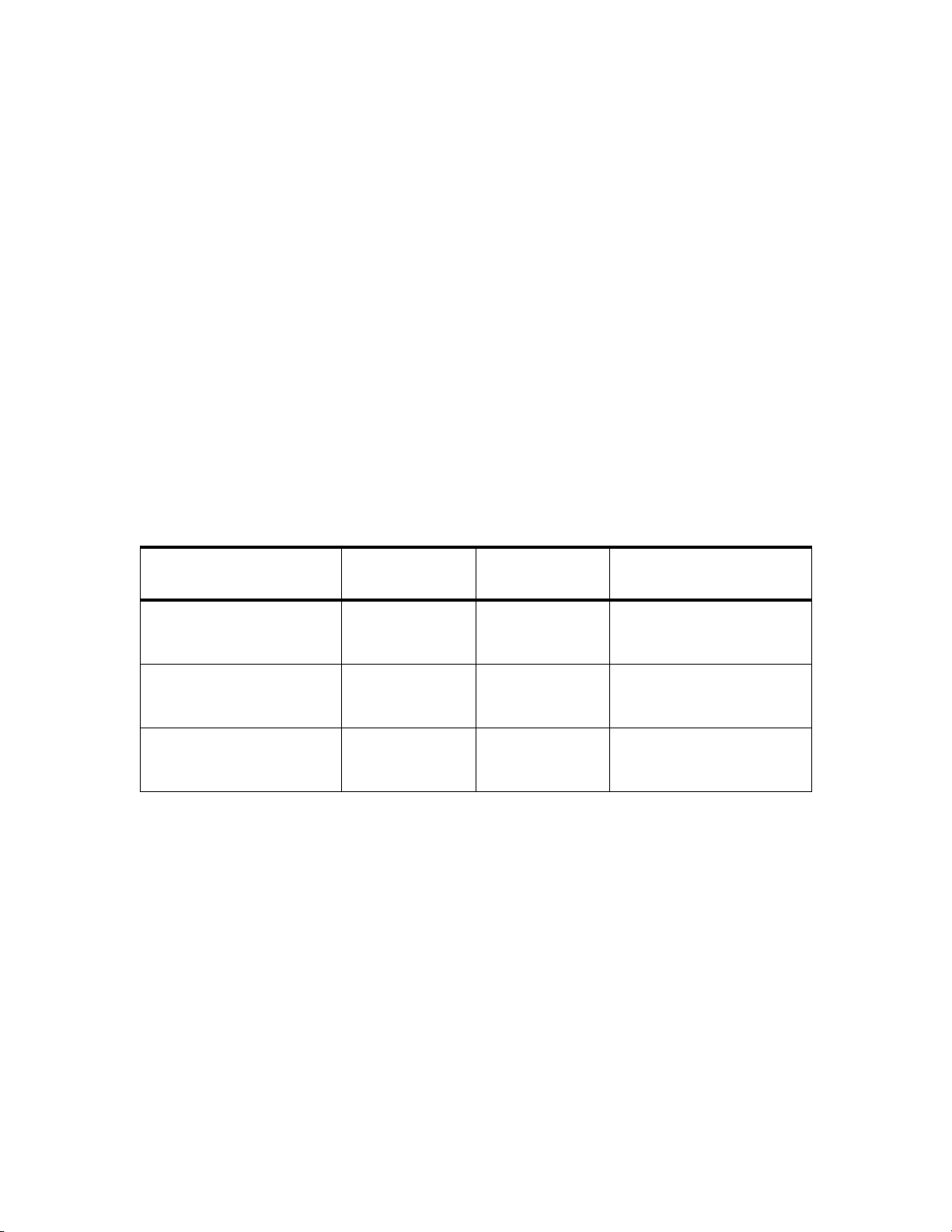
take advantage of the MCF5202 caching schemes. One example of implementing this would be to simply concatenate A[31:24] = $01 in front of the Þrst 24-bit address region, and control the caching scheme for this region using
ACR0. Then concatenate A[31:24] = $02 in front of the second 24-bit address region, which will have a separate
caching scheme, and control the caching scheme for this region with ACR1. Finally, concatenate A[31:24] = $03 in
nc...
I
front of the third 24-bit address region, which could have yet another caching scheme, and control the caching
scheme for this region using the default cache mode in the CACR register. This example memory map translation is
shown in Table 1.
Freescale Semiconductor, Inc.
cale Semiconductor,
Frees
Table 1: Example Memory Map Translation
68000 MEMORY MAP
A[23:0]
$000000
$1FFFFF
$200000
$3FFFFF
$400000
$FFFFFF
For this example, ACR0 can be set up such that everything within the region $01xxxxxx, which includes
$01000000 - $011FFFFF containing instructions, can have a speciÞc cache attribute such as copyback. ACR1 can be
set up such that everything within the region $02xxxxxx, which includes $02200000 - $023FFFFF containing data,
can have another speciÞc cache attribute such as writethrough. The CACR can be set up such that everything not
mapped by the ACRs, which includes $03400000 - $03FFFFFF containing I/O, can have a third cache attribute such
as cache inhibit. Now, when the software code is compiled, the new MCF5202 memory map that is speciÞc to the
customerÕs system must be used when assigning the corresponding instruction, data, and I/O sections.
CONTENTS CACHE CONTROL
Instructions ACR0
Data ACR1
I/O CACR
5202 MEMORY MAP
A[31:0]
$01000000
$011FFFFF
$02200000
$023FFFFF
$03400000
$03FFFFFF
2.1.2 Cache Coherency
If the MCF5202 has its cache on and in copyback mode, and if there is another bus master in the system that
can arbitrate the system bus away from the MCF5202 and modify a shared piece of memory, users should be careful
about maintaining cache coherency. Cache coherency is the term used to describe the act of keeping the on-chip
cache consistent (or coherent) with external memory, if other masters will be using the same memory. Refer to the
ÒCache CoherencyÓ section of the ColdFire MCF5202 UserÕs Manual . If cache coherency is required, then the simplest way to resolve this problem is to control the shared memory region with one of the ACRs and set this ACRÕs
2 GATEWAY BOARD MOTOROLA
For More Information On This Product,
Go to: www.freescale.com
Page 3

cache mode to cache-inhibit. This will require the microprocessor to go to external memory to get accurate data as
opposed to having a cache hit within internal memory which could possibly contain stale data.
2.1.3 RMW cycles
If the TAS instruction is used in the original M68000 code for implementing the locked or read-modify-write
transfer sequence in hardware, then new code will have to be written that essentially implements the same locked
transfer in software. This can be done by raising the interrupt mask to 7 and then executing the read, modify, and
write instructions, and then lowering the mask back down to the appropriate level. This will ensure that the sequence
of instructions between the raising and lowering of the mask will execute uninterrupted, except for a level 7 interrupt
which is nonmaskable.
Freescale Semiconductor, Inc.
2.2 Hardware Considerations
The target system must have a female 68-pin PLCC socket such that it could hold a 68EC000 PLCC FN package not a 68EC000 QFP FU package. The Gateway board has a male connector arranged in a PLCC FN fashion that
will sit in this socket. The Gateway board can operate in 8- or 16-bit data mode. The board can handle interrupt
acknowledge cycles for external vector number acquisition or the AVEC* signal can be used to allow internal vector
nc...
I
generation. One difference between the MCF5202 and the 68EC000 is that DA*[1:0] is always asserted whether
AVEC* is asserted or not. Also, the interrupt level being acknowledged is driven onto A/D[4:2] by the MCF5202,
which has to be routed onto address lines A[3:1] for the 68EC000. See Figure 3 for more details. The board also has
control logic to handle bus arbitration for alternate bus masters. If the HALT signal is asserted, the processor will
stop bus activity at the completion of the current bus cycle and will place all control signals in the inactive state and
place all three-state lines in the high-impedance state.
cale Semiconductor,
Frees
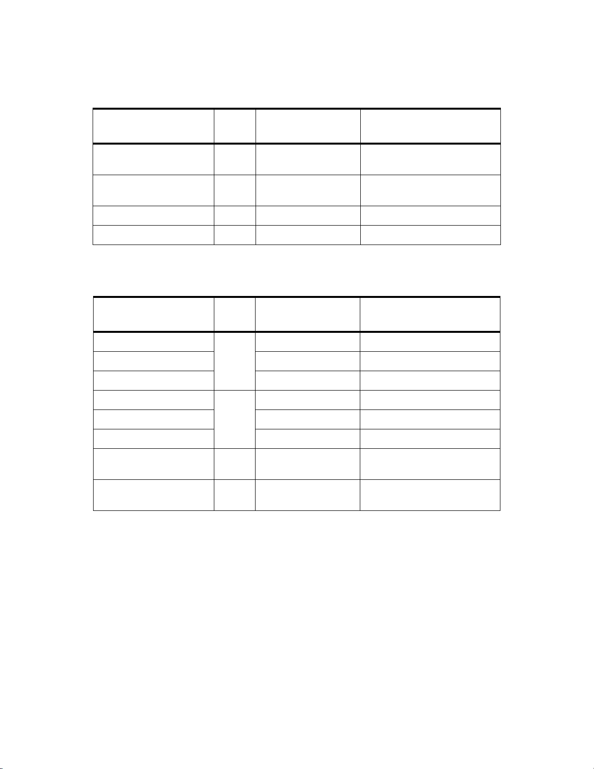
3.0 Performance
The Gateway board performance will be Þrst discussed generally and then speciÞcally with an industry-standard benchmark. For each bus cycle, there is one extra clock required from the beginning of the ColdFire MCF5202
microprocessor bus cycle to the beginning of the 68EC000 bus cycle. This is due to the multiplexed ATM signal on
the ColdFire which is required to create the FC signals on the 68EC000 bus. Also, there are some bus clocks inherent
to the ColdFire cycle that occur after the 68EC000 bus cycle is done. This is zero to two extra clocks, depending on
the size of the access and whether the access is a read or a write. Therefore, because the fastest possible bus transaction for the 68EC000 is 4 bus clocks, the fastest Gateway board bus transaction can be as few as 5 bus clocks for the
Þrst bus access of a longword write, or as many as 7 bus clocks if doing, for example, a single byte read. Table 2 and
Table 3,compare all possible combinations of accesses between the MCF5202 and the MC68EC000.
MOTOROLA GATEWAY BOARD 3
For More Information On This Product,
Go to: www.freescale.com
Page 4
Freescale Semiconductor, Inc.
Table 2: Bus Clock Timing Comparison (16-bit mode)
MCF5202 DATA ACCESS
Byte, Word
Long
Byte, Word
Long
Line Fill (4 Longs) Read 6+6+6+6+6+6+6+7=49 4+4+4+4+4+4+4+4=32
Line Fill (4 Longs) Write 5+5+5+5+5+5+5+7=42 4+4+4+4+4+4+4+4=32
nc...
I
MCF5202 DATA ACCESS
Byte
Word 6+7=13 4+4=8
Long 6+6+6+7=25 4+4+4+4=16
Byte
Word 5+7=12 4+4=8
Long 5+5+5+7=22 4+4+4+4=16
Line Fill (4 Longs) Read 6+6+6+6+6+6+6+6+
cale Semiconductor,
Line Fill (4 Longs Write 5+5+5+5+5+5+5+5+
Table 3: Bus Clock Timing Comparison (8-bit mode)
READ/
WRITE
Read 7
Write 7
READ/
WRITE
Read
Write
GATEWAY BOARD
BUS CLOCKS
6+7=13
5+7=12
GATEWAY BOARD
BUS CLOCKS
74
74
6+6+6+6+6+6+6+7=97
5+5+5+5+5+5+5+7=82
EQUIVALENT MC68EC000 BUS
CLOCKS TO GET SAME DATA
4
4+4=8
4
4+4=8
EQUIVALENT MC68EC000 BUS
CLOCKS TO GET SAME DATA
4+4+4+4+4+4+4+4+
4+4+4+4+4+4+4+4=64
4+4+4+4+4+4+4+4+
4+4+4+4+4+4+4+4=64
Frees
The industry standard Dhrystone 2.1 benchmark was run on the Motorola Gateway board, as well as some other
systems, and the results are shown in Table 4. If you notice in Table 4, the Gateway board requires about a 7.5MHz
increase in frequency (12.5MHz to 20MHz) to get about the same MIPS performance of the 68EC000 evaluation
board. This is attributable to the handshaking required between the MCF5202 and the 68EC000. Notice, however, if
the internal cache of the MCF5202 is used, the MIPS performance of the system is increased dramaticallyÑmore
than 8 times better than with cache off. In addition, if system bus interface changes are made to take advantage of the
MCF5202 bus interface, such as widening the data bus and allowing bursting (which will be discussed later), even
greater system performance will result.
4 GATEWAY BOARD MOTOROLA
For More Information On This Product,
Go to: www.freescale.com
Page 5

Freescale Semiconductor, Inc.
Table 4: Dhrystone 2.1 Benchmark Performance
nc...
I
cale Semiconductor,
Frees
SYSTEM
MC68EC000 Board 16 bit 12.5 MHz 8-8-8-8-8-8-8-8 N/A 1.01
Gateway Board 8 bit 20 MHz R: 10-10-10-11-10-10-10-11-
Gateway Board 16 bit 20 MHz R: 10-11-10-11-10-11-10-11
Gateway Board 8 bit 20 MHz R: 10-10-10-10-10-10-10-10-
Gateway Board 16 bit 20 MHz R: 10-10-10-10-10-10-10-11
MCF5202 Board 32 bit 20 MHz 8-4-4-4 Copy-Back 12.6
DATA
WIDTH
FREQUENCY
10-10-10-11-10-10-10-11
W: 9- 9- 9-11- 9- 9- 9-11 9- 9- 9-11- 9- 9- 9-11
W: 9-11- 9-11- 9-11- 9-11
10-10-10-10-10-10-10-11
W: 9- 9- 9- 9- 9- 9- 9- 9 9- 9- 9- 9- 9- 9- 9-11
W: 9- 9- 9- 9- 9- 9- 9-11
DRAM ACCESSES
(TO GET 16 BYTES)
CACHE
MODE
Off 0.56
Off 1.07
Copy-Back 5.95
Copy-Back 9.12
MIPS
(@ GIVEN
FREQUENCY)
4.0 Potential Performance and System Improvements
To fully take advantage of the MCF5202 performance in a target system, the 68EC000 bus could be changed to
interface better to the MCF5202 bus. First, the maximum frequency of operation for the Gateway boardÕs MCF5202
is 33MHz, which can be a substantial improvement over the 12.5MHz, 16.7MHz, or even the 20MHz version of the
68EC000. So, if the 68EC000 system was designed to operate at higher frequencies, this would be an easy way to
increase overall system performance. Second, the 16-bit 68EC000 data bus could be widened to 32-bits so that the
MCF5202 can get a longword in one bus transaction instead of the two bus transactions that are required now through
the Gateway board. Three, when the MCF5202 does a burst access (gives one address, expects 4 longwords of data),
if the 68EC000 system could be changed to provide the secondary 3 longwords faster than the full bus transaction
required by the current 68EC000 system, the overall MCF5202 performance can be improved dramatically. For
example, if the data bus was widened to 32-bits and page mode DRAM was used in the system, the MCF5202 could
potentially do a cache line Þll (4 longwords) in 7 bus clocks (4-1-1-1) instead of 49 bus clocks (6-6-6-6-6-6-6-7).
The MCF5202 was chosen for the Gateway board because of its on-chip 2KB uniÞed cache that allows customers to experiment among various on-chip memory conÞgurations. For example, the 2KB uniÞed cache can be conÞgured to be 2KB of I-cache only, 2KB of D-cache only, 1KB of I-cache and 1KB of D-cache, or as a normal 2KB
uniÞed cache with a dynamic mixture of both instructions and data. Other ColdFire microprocessors can be selected
according to speciÞc system requirements. For example, the MCF5204, which would not require latches and buffers
because it has a demultiplexed address and data bus (just like the 68EC000) has a little less on-chip memory (512
byte I-cache and 512 byte SRAM) compared to the MCF5202. Therefore, using the MCF5204 would most likely
give a little less performance, but would save overall system cost.
5.0 Debug Support
There is a ColdFire BDM connector (labeled J2) on the Gateway board that is a 26-pin Berg Connector
arranged in two rows of thirteen pins each. This connector is commonly used by software debugger vendors to allow
such features as real-time trace, real-time debug, and background debug.
MOTOROLA GATEWAY BOARD 5
For More Information On This Product,
Go to: www.freescale.com
Page 6

Freescale Semiconductor, Inc.
6.0 Bus Operation
The Gateway board supports a synchronous interface between the MCF5202 bus and the MC68EC000 bus.
The waveforms in this document are meant to provide a functional description of the bus cycles required for data
transfer operations. The examples below show a longword read and write to a 16-bit wide data bus of the
MC68EC000 as well as an Interrupt Acknowledge Cycle. Note that at all times the MCF5202 will not burst
(TBI*=0) and that the address phase lasts for only one clock (AA*=0).
Figure 1: Longword Read To A 16-Bit Port
PS1
PS1 PS2 PS3 PS4 PS5 PS1 PS1
w S0S2S4S6 w w
w
CLOCK
TS*
nc...
I
R/W*
PS2 PS3 PS4 PS5 PS1 PS1wPS1
S0 S2 S4 S6 w w
cale Semiconductor,
Frees
TT[1:0]
AT M
SIZ[1:0]
AD[31:16]
AD[15:0]
DA*[1:0]
FC[2:0]
A[23:0]
AS*
UDS
LDS
DTACK*
D[15:8]
00
00
ADDR
READ D[31:16]ADDR
01 01
READ D[31:24]
10
ADDR
ADDR
READ D[15:0]
READ D[15:8]
D[7:0]
6 GATEWAY BOARD MOTOROLA
For More Information On This Product,
READ D[23:16]
Go to: www.freescale.com
READ D[7:0]
Page 7

CLOCK
TS*
R/W*
PS1
PS1 PS2 PS3 PS4 PS5 PS1
w S0S2S4S6w
w
Freescale Semiconductor, Inc.
Figure 2: Longword Write To A 16-Bit Port
PS2 PS3 PS4 PS5 PS1 PS1wPS1
S0 S2 S4 S6 w w
TT[1:0]
AT M
SIZ[1:0]
AD[31:16]
nc...
I
cale Semiconductor,
AD[15:0]
DA*[1:0]
FC[2:0]
A[23:0]
AS*
UDS
LDS
DTACK*
D[15:8]
D[7:0]
00
00
ADDR
10
WRITE D[31:16]ADDR
WRITE D[31:24]
WRITE D[23:16] WRITE D[7:0]
01
ADDR
ADDR
WRITE D[15:0]
WRITE D[15:8]
01
Frees
MOTOROLA GATEWAY BOARD 7
For More Information On This Product,
Go to: www.freescale.com
Page 8

CLOCK
TS*
R/W*
Freescale Semiconductor, Inc.
PS1
PS1 PS2 PS3 PS4 PS5 PS1 PS1
w S0S2S4S6 w w
w
Figure 3: Interrupt-Acknowledge Operation
PS1
w
PS2 PS3 PS4 PS5 PS1 PS1wPS1
S0 S2 S4 S6 w w
nc...
I
cale Semiconductor,
Frees
TT[1:0]
AT M
SIZ[1:0]
AD[31:24]
AD[23:5]
AD[4:2]
AD[1:0]
DA*[1:0]
AVEC*
IPL*[2:0]
FC[2:0]
A[23:4]
A[3:1]
A0
AS*
UDS
LDS
11
01
VECTOR
IPL
LEVEL
01 or
10
IPL LEVEL IPL LEVEL
01
IPL
LEVEL
01 or
10
DTACK*
D[15:8]
D[7:0]
(VECTOR NUMBER
ACQUISITION)
8 GATEWAY BOARD MOTOROLA
VECTOR
IACK CYCLE
(AUTOVECTORED)
For More Information On This Product,
Go to: www.freescale.com
IACK CYCLE
Page 9

Freescale Semiconductor, Inc.
7.0 PLD State Diagram
Figure 4: SimpliÞed PLD State Diagram
TS
Reset
nc...
I
cale Semiconductor,
Frees
TS
Wait
for
beginning
of ColdFire
cycle
Data
Acknowledge
to the
MCF5202
Grant
BR68K
Grant to
68EC000
Bus Master
No
BR68K
BDCF
BDCF
Grant to
ColdFire
BR68K
BR68K
No
Grant
8.0 PLD ABEL Code
MODULE gateway
TITLE 'The controlling signals between a 5202 and a 68EC000'
gateway device 'ispLSI';
pLSI property 'PART ispLSI1016-80LT44';
pLSI property 'IGNORE_FIXED_PIN OFF';
pLSI property 'PULLUP ON';
pLSI property 'Y1_AS_RESET ON';
TS
TS
DTACK
DTACK
Begin a
68EC000
cycle
Assert
other control
signals
Wait
for
Acknowledge
from
68EC000
pLSI property 'LOCK AVEC 1';
pLSI property 'LOCK HALT 2';
pLSI property 'LOCK PCLK 5';
"pLSI property 'LOCK SDI 8';
pLSI property 'LOCK TT1 9';
pLSI property 'LOCK TT0 10';
pLSI property 'LOCK ATM 11';
pLSI property 'LOCK BR68K 15';
"pLSI property 'LOCK SDO 18';
pLSI property 'LOCK SIZ1 19';
pLSI property 'LOCK BDCF 21';
"pLSI property 'LOCK SCLK 27';
"pLSI property 'LOCK RSTI 29';
MOTOROLA GATEWAY BOARD 9
For More Information On This Product,
Go to: www.freescale.com
Page 10

nc...
I
cale Semiconductor,
Frees
Freescale Semiconductor, Inc.
"pLSI property 'LOCK ISPMODE 30';
pLSI property 'LOCK AD0 38';
pLSI property 'LOCK MODE 40';
pLSI property 'LOCK SIZ0 41';
pLSI property 'LOCK RnW 42';
pLSI property 'LOCK DTACK 43';
pLSI property 'LOCK TS 44';
pLSI property 'LOCK AENORM 3';
pLSI property 'LOCK AEIACK 4';
pLSI property 'LOCK FC2 12';
pLSI property 'LOCK FC1 13';
pLSI property 'LOCK FC0 14';
pLSI property 'LOCK BG68K 16';
pLSI property 'LOCK BGCF 20';
pLSI property 'LOCK LDAT 22';
pLSI property 'LOCK OEBA8 23';
pLSI property 'LOCK OEAB8 24';
pLSI property 'LOCK OEBA16 25';
pLSI property 'LOCK OEAB16 26';
pLSI property 'LOCK UDS 31';
pLSI property 'LOCK LDS 32';
pLSI property 'LOCK ADLT 33';
pLSI property 'LOCK AS 34';
pLSI property 'LOCK DA1 35';
pLSI property 'LOCK DA0 36';
pLSI property 'LOCK AEUP 37';
"------------------------------------------------------------------------------------------
DECLARATIONS
"Inputs - All Positive Logic
!AVEC pin 1 istype 'input'; "nAVEC
!HALT pin 2 istype 'input'; "nHALT
PCLK pin 5 istype 'input'; "CLK from motherboard to uP
" pin 8 istype 'input'; SDI - only used for in-circuit programming of PLD
TT1 pin 9 istype 'input';
TT0 pin 10 istype 'input';
ATM pin 11 istype 'input';
!BR68K pin 15 istype 'input'; "nBR68K
" pin 18 istype 'input'; SDO - only used for in-circuit programming of PLD
SIZ1 pin 19 istype 'input';
!BDCF pin 21 istype 'input'; "nBDCF
" pin 27 istype 'input'; SCLK - only used for in-circuit programming of PLD
!RSTI pin istype 'input'; "pin 29 - nRSTI - RESET pin
" pin 30 istype 'input'; ISPMODE - only used for in-circuit programming of PLD
AD0 pin 38 istype 'input'; "AD0 (unlatched)
MODE pin 40 istype 'input'; "Dedicated IN3 - 0=8-bit, 1=16-bit
SIZ0 pin 41 istype 'input';
RnW pin 42 istype 'input';
!DTACK pin 43 istype 'input'; "nDTACK
!TS pin 44 istype 'input'; "nTS
"Outputs - All Positive Logic
!AENORM pin 3 istype 'output'; "Addr Enable for NORM Op - AENORM=0=HIZ, AENORM=1=output
!AEIACK pin 4 istype 'output'; "Addr Enable for IACK Op - AEIACK=0=HIZ, AEIACK=1=output
FC2 pin 12 istype 'output';
FC1 pin 13 istype 'output';
FC0 pin 14 istype 'output';
10 GATEWAY BOARD MOTOROLA
For More Information On This Product,
Go to: www.freescale.com
Page 11

Freescale Semiconductor, Inc.
!BG68K pin 16 istype 'output'; "nBG68K
!BGCF pin 20 istype 'output'; "nBGCF
LDAT pin 22 istype 'output'; "(!nLE16_8) - 0=transparent latches, L-2-H=latches data
!OEBA8 pin 23 istype 'output'; "nOEBA8 =0=HIZ, 1=output from B (TDAT) to A (AD) enabled
!OEAB8 pin 24 istype 'output'; "nOEAB8 =0=HIZ, 1=output from A (AD) to B (TDAT) enabled
!OEBA16 pin 25 istype 'output'; "nOEBA16=0=HIZ, 1=output from B (TDAT) to A (AD) enabled
!OEAB16 pin 26 istype 'output'; "nOEAB16=0=HIZ, 1=output from A (AD) to B (TDAT) enabled
!UDS pin 31 istype 'output'; "nUDS
!LDS pin 32 istype 'output'; "nLDS
!ADLT pin 33 istype 'output'; "Addr Latch - 0=transparent latches, L-2-H=latches data
!AS pin 34 istype 'output'; "nAS
!DA1 pin 35 istype 'output'; "nDA1
!DA0 pin 36 istype 'output'; "nDA0
!AEUP pin 37 istype 'output'; "Addr Enable for A[23:8] - AEUP=0=HIZ, AEUP=1=output
"-----------------------------------------------------------------------------------------
"Internal Nodes
nc...
I
cale Semiconductor,
Frees
PQ0,PQ1,PQ2 node istype 'reg, buffer';
A0 node istype 'reg,buffer';
ATMA node istype 'reg,buffer';
NQ1 node istype 'reg';
NQ2 node istype 'reg';
NCLK node;
BQ0,BQ1 node istype 'reg,buffer';
"Constants
c,k,x,z = .C.,.K.,.X.,.Z.; "this is used for test vectors
"State Value Constants
psreg = [PQ2,PQ1,PQ0]; "Positive Clk State Register
PS0 = [0,0,0]; "!PQ2&!PQ1&!PQ0
PS1 = [0,0,1]; "!PQ2&!PQ1&PQ0
PS2 = [0,1,1]; Ò!PQ2&PQ1&PQ0
PS3 = [0,1,0]; "!PQ2&PQ1&!PQ0
PS4 = [1,1,0]; "PQ2&PQ1&!PQ0
PS5 = [1,0,0]; "PQ2&!PQ1&!PQ0
PSTATE0 = !PQ2&!PQ1&!PQ0;
PSTATE1 = !PQ2&!PQ1&PQ0;
PSTATE2 = !PQ2&PQ1&PQ0;
PSTATE3 = !PQ2&PQ1&!PQ0;
PSTATE4 = PQ2&PQ1&!PQ0;
PSTATE5 = PQ2&!PQ1&!PQ0;
bsreg = [BQ1,BQ0]; "BusArb State Register
BS0 = [0,0];
BS1 = [0,1];
BS2 = [1,1];
BS3 = [1,0];
Equations
"Initializations
psreg.clk = PCLK;
psreg.ar = RSTI;
A0.clk = TS; "AD0 is latched when TS is asserted
MOTOROLA GATEWAY BOARD 11
For More Information On This Product,
Go to: www.freescale.com
Page 12

ATMA.clk = TS; "ATM is latched when TS is asserted
NQ1.ar = RSTI;
NQ2.ar = RSTI;
NQ1.clk= PCLK; "Clock NegClk machine 1 with pos clk
NQ2.clk= !PCLK; "Clock NegClk machine 2 with the inverted pos clk
bsreg.clk = PCLK;
bsreg.ar = RSTI;
"Output enables
AS.oe = !BG68K; Òenable when the 68K is not granted the bus
UDS.oe = !BG68K; Òenable when the 68K is not granted the bus
LDS.oe = !BG68K; "enable when the 68K is not granted the bus
FC0.oe = !BG68K; "enable when the 68K is not granted the bus
FC1.oe = !BG68K; "enable when the 68K is not granted the bus
FC2.oe = !BG68K; "enable when the 68K is not granted the bus
Freescale Semiconductor, Inc.
nc...
I
cale Semiconductor,
Frees
"Sequential Logic
A0 := AD0;
ATMA := ATM;
NQ1 := !NQ1;
NQ2 := NQ1;
"-----------------------------------------------------------------------------------------
"Combinational Logic - (See NOTE 2)
NCLK = NQ1 !$ NQ2; "XNOR the outputs of the two NegClk state machines to produce NCLK
" AS is asserted for PS3, PS4, and the posclk of PS5
AS = PSTATE3 # PSTATE4 # PSTATE5&!NCLK;
" OEBA16 = (CF is master & not halted & during AS)&(16-bit read & !IACK)
OEBA16 = (!BG68K & !HALT & AS) & ( RnW&MODE & !(TT1 & TT0) );
" OEBA8 = (CF is master & not halted & during AS)&(8-bit read # IACK)
OEBA8 = (!BG68K & !HALT & AS) & ( RnW&!MODE # TT1&TT0 );
" OEAB16 = (CF is master & not halted & during AS)&(16-bit write)
OEAB16 = (!BG68K & !HALT & AS) & ( !RnW&MODE );
" OEAB8 = (CF is master & not halted & during AS)&(8-bit write
OEAB8 = (!BG68K & !HALT & AS) & ( !RnW&!MODE );
" UDS = (Read&PS3 # PS4 # PCLK&PS5) & (16-bit) & !( Odd & Byte )
UDS = (RnW&PSTATE3 # PSTATE4 # PSTATE5&!NCLK) & MODE & !( A0 & !SIZ1&SIZ0 );
" LDS = (Read&PS3 # PS4 # PCLK&PS5) & !(16-bit & Even & Byte & !IACK)
LDS = (RnW&PSTATE3 # PSTATE4 # PSTATE5&!NCLK) & !( MODE & !A0 & !SIZ1&SIZ0 & !(TT1&TT0) );
DA1 = PSTATE5 & MODE; "PS5 & 16-bit
DA0 = PSTATE5 & !MODE; "PS5 & !16-bit
LDAT = PSTATE5 & NCLK; "PS5 & NCLK
"ADLT = (TS&PS1 # PS2 # PS3 # PS4 # PCLK&PS5)
ADLT = (TS&PSTATE1 # PSTATE2 # PSTATE3 # PSTATE4 # PSTATE5&!NCLK);
AENORM = (!BG68K & !HALT) & !(TT1&TT0); "(CF is master & not halted) & !(IACK-Access)
AEIACK = (!BG68K & !HALT) & (TT1&TT0); "(CF is master & not halted) & (IACK-Access)
AEUP = (!BG68K & !HALT); "(CF is master & not halted)
12 GATEWAY BOARD MOTOROLA
For More Information On This Product,
Go to: www.freescale.com
Page 13

Freescale Semiconductor, Inc.
"Function Codes for EC000 - (See NOTE 1)
" FC2 = ( (ATM & Normal-Access) # (IACK-Access) )
FC2 = ( ATM # (TT1&TT0) );
" FC1 = ( (ATMA & Normal-Access) # (IACK-Access) )
FC1 = ( ATMA # (TT1&TT0) );
" FC0 = ( (!ATMA & Normal-Access) # (IACK-Access) )
FC0 = ( !ATMA # (TT1&TT0) );
"-----------------------------------------------------------------------------------------
STATE_DIAGRAM psreg;
STATE PS0: "RESET and waiting for TS to de-assert
IF TS THEN PS0; "Wait for TS to de-assert
ELSE PS1;
nc...
I
cale Semiconductor,
Frees
STATE PS1: "Waiting for TS to assert, Beginning of ColdFire cycle
IF !TS THEN PS1; "Waiting for TS to assert
ELSE PS2;
STATE PS2: "Beginning of 68K cycle, assert FCÕs and Address
IF HALT THEN PS2; ÒIf HALT is asserted then stay in state 2
ELSE PS3; "else goto state 3
STATE PS3: "Assert other control signals
GOTO PS4; "Unconditionally goto state 4
STATE PS4: "Waiting for DTACK from 68K
IF (TT1 & TT0 & AVEC) THEN "if TT[1:0]=11 (IACK and AVEC) then
PS5; "goto state 5 (just DA the cycle)
ELSE
IF (DTACK) THEN "else if (Normal or IACK without AVEC), look for DTACK
PS5; "goto state 5
ELSE
PS4; "else stay in state 4
STATE PS5: "Data acknowledge to ColdFire
GOTO PS1; "Unconditionally goto state 1
"------------------------------------------------------------------------------------------
STATE_DIAGRAM bsreg;
STATE BS0: "Give the bus to CF, and wait for Request
BGCF=1; "Assert Grant to CF
BG68K=0; "Do not assert Grant to 68K
IF BR68K THEN "If there is a Bus Request,
BS1; "goto state 1
ELSE "else if no request,
BS0; "stay in state 0
MOTOROLA GATEWAY BOARD 13
For More Information On This Product,
Go to: www.freescale.com
Page 14

Freescale Semiconductor, Inc.
STATE BS1: "Got a Request, wait for CF to quit driving the bus
BGCF=0; BG68K=0; "Do not assert either Grant
IF !BDCF THEN "If CF is not driving the bus,
BS2; "then goto state 2
ELSE "else if CF is driving the bus,
BS1; "stay in state 1
STATE BS2: "Done driving the bus, give the bus to 68K, wait for
Request to go away
BGCF=0; "Do not assert Grant to CF
BG68K=1; "Assert Grant to 68K
IF BR68K THEN "If 68K is still requesting the bus,
BS2; "then stay in state 2
ELSE "else if no longer requesting the bus,
BS3; "goto state 3
STATE BS3: "Request went away, delay one clock, then bus back to CF
BGCF=0; BG68K=0; "Do not assert either Grant
nc...
I
GOTO BS0; "goto state 0
cale Semiconductor,
Frees
"------------------------------------------------------------------------------------------"NOTE 1:
" ATMa ATMd TT1 TT0 FC2 FC1 FC0 Notes
"
"0000001Normal User Data
"1000010Normal User Instruction
"0100101Normal Supervisor Data
"1100110Normal Supervisor Instruction
"XX01000Reserved
"XX10???Emulator Access
"XX11111CPU Space or IACK
"NOTE 2:
"RnW MODE A0 (!SIZ1& AENORM AEIACK UDS LDS OExxxx Notes
" SIZ0)
" 1 1 0 1 1 0 1 0 OEBA16 Read,16-bit,even,byte,Normal
" 1 1 0 1 0 1 1 1 OEBA8 Read,16-bit,even,byte,IACK
" 1 1 0 0 x x 1 1 OEBA16 Read,16-bit,even,!byte
" 1 1 1 1 x x 0 1 OEBA16 Read,16-bit,odd, byte
" 1 1 1 0 x x 1 1 OEBA16 Read,16-bit,odd,!byte (N/A)
" 1 0 x x x x 0 1 OEBA8 Read,8-bit
" 0 1 0 1 x x 1 0 OEAB16 Write,16-bit,even,byte
" 0 1 0 0 x x 1 1 OEAB16 Write,16-bit,even,!byte
" 0 1 1 1 x x 0 1 OEAB16 Write,16-bit,odd,byte
" 0 1 1 0 x x 1 1 OEAB16 Write,16-bit,odd,!byte (N/A)
" 0 0 x x x x 0 1 OEAB8 Write,8-bit
END
14 GATEWAY BOARD MOTOROLA
For More Information On This Product,
Go to: www.freescale.com
Page 15

9.0 Block Diagram
Freescale Semiconductor, Inc.
Figure 5: Gateway Board Block Diagram
68EC000
Connector
(68-pin PLCC)
A
B
D
ColdFire
MCF5202
PLD
M
A/D
nc...
I
10.0 Gateway Board Physical Layout
Figure 6: Physical Layout (Actual Size )
Component Side Solder Side
ISP
J3
U7
U8
9
10
26
U6
1
J1
U9
61
60
44
ColdFire Gateway Board
S/N
3.5 in.
cale Semiconductor,
U2
U1
D
61
60
44
43
J1
9
1
10
J3
26
27
Frees
2
BDM
1
U4
U5
J2
U3
26
25
J2
2 in.
MOTOROLA GATEWAY BOARD 15
For More Information On This Product,
Go to: www.freescale.com
Page 16

Freescale Semiconductor, Inc.
11.0 Gateway Board Bill Of Material
Table 5: Bill Of Material
ITEM QTY MANUFACTURER PART NO. REF. DES. DESCRIPTION
1 1 Motorola XCF5202PU33A U1 IC, MCF5202, 33 MHz, 100pin, TQFP
2 1 Lattice ISPLSI1016-90LT44 U2 IC, PLD, 44 pins, TQFP
3 4 Motorola MC74F573DW U3-U5, U9 IC, 74F573, 20 pins, SOL20
4 3 Motorola MC74F543DW U6-U8 IC, 74F543, 24 pins, SOL24
5 4 Venkel CR1206-8W-103JT R1-R4 Res, 10K, 5%, 1/8W, 1206
6 4 Venkel CR1206-8W-472JT R5-R8 Res, 4.7K, 5%, 1/8W, 1206
7 4 Samtec TMS-117-55-G-S J1 Conn, HDR, 17 pins, 50Mil ctr, single row, 1X17
nc...
I
cale Semiconductor,
Frees
8 1 AMP 1-103783-3 J2 Conn, HDR, 26 pins, 100Mil ctr, dual row, 2X13
9 1 AMP 1-87499-3 J3 Conn, HDR, 8 pins, 100Mil ctr, single row, 1X8
10 1 Samwa
Venkel
11 1 Panasonic S1012-36-ND C2 Cap, 33UF, 10%, 16V, 1206, TANT
12 22 Samwa
Venkel
13 1 Samwa
Venkel
CS3216X7R103K500R
C1206X7R500-103KNE
CS3216X7R104K500R
C1206X7R500-104KNE
CS3216COG100K500R
C1206C0G500-100JNE
C1 Cap, 0.01UF, 10%, 50V, 1206
C3-C24 Cap,0.1UF, 10%, 50V, 1206
C25 Cap, 10PF, 10%, 50V, 1206
16 GATEWAY BOARD MOTOROLA
For More Information On This Product,
Go to: www.freescale.com
Page 17

nc...
I
cale Semiconductor,
Frees
Freescale Semiconductor, Inc.
12.0 ColdFire Gateway Board Schematics (1 of 2)
U1
MCF5202
AD8
AD9
AD5
AD2
AD3
AD4
AD5
AD5
AD6
AD7
AD0
AD1
AD2
AD3
AD4
AD5
AD6
AD7
1
11
2
3
4
5
6
7
8
9
1
11
2
3
4
5
6
7
8
9
1
11
2
3
4
5
6
7
8
9
1
11
2
3
4
5
6
7
8
9
nIPL1
nIPL2
ISPEN
CLK
nRST
BKPT
DSI
DSO
DSCLK
DDATA0
DDATA1
DDATA2
DDATA3
PST0
PST1
PST2
PST3
GND
VCC
GND
GND
VCC
AD0
AD1
AD2
AD3
AD4
AD5
AD6
AD7
AD8
AD9
AD10
AD11
AD12
AD13
AD14
AD15
AD16
AD17
AD18
AD19
AD20
AD21
AD22
AD23
AD24
AD25
AD26
AD27
AD28
AD29
AD30
AD31
nRST
nTEA
BKPT
87
67
74
73
72
71
70
81
82
83
84
56
57
58
59
85
76
77
78
75
89
90
91
92
95
96
97
98
1
2
3
4
5
8
9
10
11
14
15
16
17
20
21
22
23
26
27
28
29
30
33
34
4.7K
10K
10K
CLK
RST
TCK
TMS/BKPT
TDI/DSI
TDO/DSO
TRST/DSCLK
DDATA0
DDATA1
DDATA2
DDATA3
PST0
PST1
PST2
PST3
JCE
MTMOD0
MTMOD1
MTMOD2
HIZ
A/D0
A/D1
A/D2
A/D3
A/D4
A/D5
A/D6
A/D7
A/D8
A/D9
A/D10
A/D11
A/D12
A/D13
A/D14
A/D15
A/D16
A/D17
A/D18
A/D19
A/D20
A/D21
A/D22
A/D23
A/D24
A/D25
A/D26
A/D27
A/D28
A/D29
A/D30
A/D31
VCC
VCC
VCC
R/W
TT0
TT1
SIZ0
SIZ1
AT M
AA
DTIP
DA0
DA1
TEA
TBI
BR
BD
BG
IPL0
IPL1
IPL2
AVEC
GND
GND
GND
GND
GND
GND
GND
GND
GND
GND
GND
GND
GND
GND
VCC
VCC
VCC
VCC
VCC
VCC
VCC
VCC
VCC
VCC
VCC
VCC
VCC
VCC
nBGCF
TS
nIPL0
DSI
100
AEUPPER
39
RNW
35
TT0
36
TT1
41
SIZ0
42
SIZ1
63
AT M
40
nTS
48
GND
47
43
nDA0
44
nDA1
55
nTEA
54
GND
50
49
nBDCF
51
nBGCF
64
nIPL0
65
nIPL1
66
nIPL2
62
nAVEC
6
GND
12
GND
18
GND
24
GND
31
GND
37
GND
45
GND
52
GND
61
GND
68
GND
79
GND
86
GND
93
GND
99
GND
7
VCC
13
VCC
19
VCC
25
VCC
32
VCC
38
VCC
46
VCC
53
VCC
60
VCC
69
VCC
80
VCC
88
VCC
94
VCC
VCC
4.7K
4.7K
10K
ADLT
AD16
AD17
AD18
AD19
AD20
AD21
AD22
AD23
AEUPPER
ADLT
AD10
AD11
AD12
AD13
AD14
AD15
AEIACK
ADLT
AENORM
ADLT
VCC
VCC
VCC
U9
74F573
OE
C
D0
D1
D2
D3
D4
D5
D6
D7
U3
74F573
OE
C
D0
D1
D2
D3
D4
D5
D6
D7
U5
74F573
OE
C
D0
D1
D2
D3
D4
D5
D6
D7
U4
74F573
OE
C
D0
D1
D2
D3
D4
D5
D6
D7
Q0
Q1
Q2
Q3
Q4
Q5
Q6
Q7
Q0
Q1
Q2
Q3
Q4
Q5
Q6
Q7
Q0
Q1
Q2
Q3
Q4
Q5
Q6
Q7
Q0
Q1
Q2
Q3
Q4
Q5
Q6
Q7
4.7K
4.7K
10K
0.01UF
10 PF
33 UF
0.1 UF
0.1 UF
0.1 UF
0.1 UF
0.1 UF
0.1 UF
0.1 UF
0.1 UF
0.1 UF
0.1 UF
0.1 UF
0.1 UF
0.1 UF
0.1 UF
0.1 UF
0.1 UF
0.1 UF
0.1 UF
0.1 UF
0.1 UF
0.1 UF
0.1 UF
GND
GND
GND
GND
GND
GND
GND
GND
GND
GND
GND
GND
GND
GND
GND
GND
GND
GND
GND
GND
GND
GND
GND
GND
GND
BYPASS FOR U1
BYPASS FOR U2 - U9
ISPEN
19
A16
18
A17
17
A18
16
A19
15
A20
14
A21
13
A22
12
A23
19
A8
18
A9
17
A10
16
A11
15
A12
14
A13
13
A14
12
A15
19
A0
18
A1
17
A2
16
A3
15
A4
14
A5
13
A6
12
A7
19
A0
18
A1
17
A2
16
A3
15
A4
14
A5
13
A6
12
A7
VCC
VCC
VCC
VCC
VCC
VCC
VCC
VCC
VCC
VCC
VCC
VCC
VCC
VCC
VCC
VCC
VCC
VCC
VCC
VCC
VCC
VCC
VCC
VCC
VCC
VCC
VCC
MOTOROLA GATEWAY BOARD 17
For More Information On This Product,
Go to: www.freescale.com
Page 18

nc...
I
cale Semiconductor,
Frees
Freescale Semiconductor, Inc.
ColdFire Gateway Board Schematics (2 of 2)
J1 / B
EC000 CONN
10
11
12
13
14
15
16
17
18
19
20
21
22
23
24
25
26
VCC
SDO
SDI
ISPEN
ISPMODE
GND
SCLK
44
nTS
43
nDTACK
42
RNW
41
SIZ0
40
MODE
39
GND
38
AD0
37
AEUPPER
36
nDA0
35
nDA1
34
nAS
33
ADLT
32
LDS
31
UDS
30
ISPMODE
29
nRST
28
VCC
27
SCLK
26
nOEAB16
25
nOEBA16
24
nOEAB8
23
nOEBA8
nIPL0
FC2
FC1
FC0
A0
A1
A2
A3
GND
A4
A5
A6
A7
A8
A9
A10
A11
J3
ISP CONN
1
2
3
4
5
6
7
8
D12
D11
D10
D9
D8
D7
D6
D5
GND
D4
D3
D2
D1
D0
nAS
UDS
LDS
GND
GND
nRST
VCC
GND
PST2
PST0
DDATA2
DDATA0
GND
VCC
nAVEC
nHALT
AENORM
AEIACK
CLK
VCC
ISPEN
TT1
TT0
AT M
FC2
FC1
FC0
nBR68K
nBG68K
GND
SDO
SIZ1
nBGCF
nBDCF
nLE16_8
SDI
J1 / A
EC000 CONN
61
62
63
64
65
66
67
68
1
2
3
4
5
6
7
8
9
J2
BDM CONN
1
3
5
7
9
11
13
15
17
19
21
23
25
1
I/O 28
2
I/O 29
3
I/O 30
4
I/O 31
5
Y0
6
VCC
7
ISPEN/NC
8
SDI/IN 0
9
I/O 0
10
I/O 1
11
I/O 2
12
I/O 3
13
I/O 4
14
I/O 5
15
I/O 6
16
I/O 7
17
GND
18
SDO/IN 1
19
I/O 8
20
I/O 9
21
I/O 10
22
I/O 11
2
4
6
8
10
12
14
16
18
20
22
24
26
ISPLSI-1016
RNW
nDTACK
nBG68K
nBR68K
VCC
VCC
CLK
GND
GND
MODE
nHALT
nRST
nAVEC
nTEA
nIPL2
nIPL1
BKPT
DSCLK
DSI
DSO
PST3
PST1
DDATA3
DDATA1
GND
CLK
nTEA
U2
I/O 27
I/O 26
I/O 25
I/O 24
IN 3
GND
I/O 23
I/O 22
I/O 21
I/O 20
I/O 19
I/O 18
I/O 17
I/O 16
IN 2/MODE
Y1/RESET
VCC
Y2/SCLK
I/O 15
I/O 14
I/O 13
I/O 12
J1 / C
EC000 CONN
27
28
29
30
31
32
33
34
35
36
37
38
39
40
41
42
43
nOEAB16
GND
nLE16_8
AD16
AD17
AD18
AD19
AD20
AD21
AD22
AD23
nOEAB16
GND
nLE16_8
AD24
AD25
AD26
AD27
AD28
AD29
AD30
AD31
nOEAB8
GND
nLE16_8
AD24
AD25
AD26
AD27
AD28
AD29
AD30
AD31
J1 / D
EC000 CONN
A12
A13
A14
A15
A16
A17
A18
A19
A20
VCC
A21
A22
A23
GND
D15
D14
D13
U6
74F543
13
OEAB
11
EAB
14
LEAB
3
A0
4
A1
5
A2
6
A3
7
A4
8
A5
9
A6
10
A7
U7
74F543
13
OEAB
11
EAB
14
LEAB
3
A0
4
A1
5
A2
6
A3
7
A4
8
A5
9
A6
10
A7
U8
74F543
13
OEAB
11
EAB
14
LEAB
3
A0
4
A1
5
A2
6
A3
7
A4
8
A5
9
A6
10
A7
OEBA
EBA
LEBA
OEBA
EBA
LEBA
OEBA
EBA
LEBA
B0
B1
B2
B3
B4
B5
B6
B7
B0
B1
B2
B3
B4
B5
B6
B7
B0
B1
B2
B3
B4
B5
B6
B7
44
45
46
47
48
49
50
51
52
53
54
55
56
57
58
59
60
23
22
21
20
19
18
17
16
15
23
22
21
20
19
18
17
16
15
23
22
21
20
19
18
17
16
15
2
1
2
1
2
1
nOEBA16
GND
nLE16_8
D0
D1
D2
D3
D4
D5
D6
D7
nOEBA16
GND
nLE16_8
D8
D9
D10
D11
D12
D13
D14
D15
nOEBA8
GND
nLE16_8
D0
D1
D2
D3
D4
D5
D6
D7
18 GATEWAY BOARD MOTOROLA
For More Information On This Product,
Go to: www.freescale.com
Page 19

Freescale Semiconductor, Inc.
nc...
I
cale Semiconductor,
Frees
Motorola reserves the right to make changes without further notice to any products herein. Motorola makes no warranty, representation or guarantee regarding
the suitability of its products for any particular purpose, nor does Motorola assume any liability arising out of the application or use of any product or circuit, and
speciÞcally disclaims any and all liability, including without limitation consequential or incidental damages. ÒTypicalÓ parameters can and do vary in different
applications. All operating parameters, including ÒTypicalsÓ must be validated for each customer application by customerÕs technical experts. Motorola does not
convey any license under its patent rights nor the rights of others. Motorola products are not designed, intended, or authorized for use as components in systems
intended for surgical implant into the body, or other applications intended to support or sustain life, or for any other application in which the failure of the Motorola
product could create a situation where personal injury or death may occur. Should Buyer purchase or use Motorola products for any such unintended or
unauthorized application, Buyer shall indemnify and hold Motorola and its ofÞcers, employees, subsidiaries, afÞliates, and distributors harmless against all claims,
costs, damages, and expenses, and reasonable attorney fees arising out of, directly or indirectly, any claim of personal injury or death associated with such
unintended or unauthorized use, even if such claim alleges that Motorola was negligent regarding the design or manufacture of the part. Motorola and are
registered trademarks of Motorola, Inc. Motorola, Inc. is an Equal Opportunity/AfÞrmative Action Employer.
MOTOROLA GATEWAY BOARD 19
For More Information On This Product,
Go to: www.freescale.com
 Loading...